
Subscribe to Our Youtube Channel
Related Manuals for Quectel FC908A


Summary of Contents for Quectel FC908A
- Page 1 FC908A Hardware Design Wi-Fi&Bluetooth Module Series Version: 1.0.0 Date: 2021-12-03 Status: Preliminary...
- Page 2 Wi-Fi&Bluetooth Module Series At Quectel, our aim is to provide timely and comprehensive services to our customers. If you require any assistance, please contact our headquarters: Quectel Wireless Solutions Co., Ltd. Building 5, Shanghai Business Park Phase III (Area B), No.1016 Tianlin Road, Minhang District, Shanghai...
- Page 3 Privacy Policy To implement module functionality, certain device data are uploaded to Quectel’s or third-party’s servers, including carriers, chipset suppliers or customer-designated servers. Quectel, strictly abiding by the relevant laws and regulations, shall retain, use, disclose or otherwise process relevant data for the purpose of performing the service only or as permitted by applicable laws.
-
Page 4: Safety Information
Manufacturers of the cellular terminal shall notify users and operating personnel of the following safety information by incorporating these guidelines into all manuals of the product. Otherwise, Quectel assumes no liability for customers’ failure to comply with these precautions. -
Page 5: About The Document
Wi-Fi&Bluetooth Module Series About the Document Revision History Version Date Author Description 2021-12-03 Elinor WANG/Michael DU Creation of the document 1.0.0 2021-12-03 Elinor WANG/Michael DU Preliminary FC908A_Hardware_Design 4 / 49... -
Page 6: Table Of Contents
Wi-Fi&Bluetooth Module Series Contents Safety Information ............................3 About the Document ..........................4 Contents ..............................5 Table Index ..............................7 Figure Index ..............................8 Introduction ............................9 1.1. Special Mark ..........................12 Product Overview ..........................13 2.1. General Description ......................... 13 2.2. - Page 7 Wi-Fi&Bluetooth Module Series Electrical Characteristics & Reliability ................... 38 4.1. Electrical Characteristics ......................38 4.2. Digital I/O Interface Characteristics ..................39 4.3. Power Consumption ......................... 39 4.4. RF Performance ........................40 4.4.1. Conducted RF Performance of Wi-Fi ................40 4.4.2. Conducted RF Performance of Bluetooth ..............
- Page 8 Table 18: WLAN_SLP_CLK parameter recommendation ................. 30 Table 19: XO parameter definition ......................31 Table 20: Pin Definition of GPIO1/GPIO2 ....................31 Table 21: FC908A operating frequency ..................... 32 Table 22: Pin Definition of RF Antenna Interfaces..................32 Table 23: Antenna Cable Requirements ....................35 Table 24: Antenna requirements ........................
- Page 9 Wi-Fi&Bluetooth Module Series Figure Index Figure 1: Functional Diagram of FC908A ................ 错误!未定义书签。 Figure 2: Pin Assignment (Top View) ......................17 Figure 3: VBAT Circuit..........................21 Figure 4: Power-up Timing ......................... 21 Figure 5: Recommended Reference Design Circuit .................. 22 Figure 6: WLAN Application Interface Connection ..................
-
Page 10: Introduction
Wi-Fi&Bluetooth Module Series Introduction This document defines the FC908A and describes its air interfaces and hardware interfaces which are connected with your application. This document can help you quickly understand module interface specifications, electrical and mechanical details, as well as other related information of the module. Associated with application notes and user guides, you can use FC908A to design and set up applications easily. - Page 11 Important Note notice that any deviation(s) from the defined parameters of the antenna trace, as described by the instructions, require that the host product manufacturer must notify to Quectel Wireless Solutions Co., Ltd that they wish to change the antenna trace design. In this case, a Class II permissive change application is required to be filed by the USI, or the host manufacturer can take responsibility through the change in FCC ID (new application) procedure followed by a Class II permissive change application.
- Page 12 Wi-Fi&Bluetooth Module Series Le pré sent appareil est conforme aux CNR d’ ISED applicables aux appareils radio exempts de licence. L’exploitation est autorisé e aux deux conditions suivantes : (1) le dispositif ne doit pas produire de brouillage pré judiciable, et (2) ce dispositif doit accepter tout brouillage reç u, y compris un brouillage susceptible de provoquer un fonctionnement indé...
-
Page 13: Special Mark
Wi-Fi&Bluetooth Module Series l'inté grateur OEM sera chargé de ré é valuer le produit final (y compris l'é metteur) et l'obtention d'une autorisation distincte au Canada. End Product Labeling This transmitter module is authorized only for use in device where the antenna may be installed such that 20 cm may be maintained between the antenna and users. -
Page 14: Product Overview
Bluetooth 5.1 standard which enables seamless integration of WLAN and Bluetooth low energy technologies. With a SDIO 2.0 interface for WLAN, a UART and a PCM interface for Bluetooth, FC908A can provide WLAN and Bluetooth functions. 2.2. Key Features The following table describes the key features of FC908A. - Page 15 Wi-Fi&Bluetooth Module Series 2.4 GHz: ⚫ 802.11b/11 Mbps: 16 dBm ± 1.5 dBm Wi-Fi Transmitting Power ⚫ 802.11g/54 Mbps: 15 dBm ± 1.5 dBm ⚫ 802.11n/HT20 MCS7: 14 dBm ± 1.5 dBm ⚫ Wi-Fi Operation Mode ⚫ DSSS, OFDM, DBPSK, DQPSK, CCK, BPSK, QPSK, 16QAM, Wi-Fi Modulation 64QAM WLAN Application Interface...
-
Page 16: Functional Diagram
FC908A supports internal crystal or external crystal. 2.4. EVB To help customers to develop applications with FC908A, the evaluation board tools include EVB board (FC908A-M.2 and corresponding TE-A), USB 2.0 data cable, antenna and other external devices used to control and test the module. For details, see document [1]. -
Page 17: Application Interfaces
Wi-Fi&Bluetooth Module Series Application Interfaces 3.1. General Description FC908A is equipped with 44 LCC pins. The subsequent chapters will provide a detailed introduction to the following function, pins and interfaces of the module: ⚫ Power supply ⚫ WLAN application interface ⚫... -
Page 18: Pin Assignment
Wi-Fi&Bluetooth Module Series 3.2. Pin Assignment ANT_WIFI0/BT RESERVED RESERVED RESERVED RESERVED RESERVED FC908A PCM_SYNC HOST_WAKE_BT PCM_DIN BT_WAKE_HOST PCM_CLK RESERVED PCM_DOUT VBAT XTAL_IN WLAN_SLP_CLK XTAL_OUT VIN_LDO Power WLAN Bluetooth XTAL Other signals RESERVED GPIO Figure 1: Pin Assignment (Top View) NOTE 1. -
Page 19: Pin Description
Wi-Fi&Bluetooth Module Series 3.3. Pin Description The following tables show the pin description of FC908A. Table 3: I/O Parameters Definition Type Description Analog Input/Output Digital Input Digital Output Digital Input/Output Power Input Power Output Table 4: Pin Description Power Supply Pin Name Pin No. - Page 20 Wi-Fi&Bluetooth Module Series SDIO_DATA2 SDIO data bit 2/NC SDIO_DATA3 SDIO data bit 3/NC SDIO_CMD SDIO command VDDIO power domain. Supports 1-bit or 4-bit mode. SDIO_CLK SDIO clock SDIO_DATA0 SDIO data bit 0 SDIO_DATA1 SDIO data bit 1/IRQ Bluetooth Application Interface Pin Name Pin No.
-
Page 21: Power Supply
Min. Typ. Max. Unit VBAT Power supply for the module Power supply for module’s VDDIO 1.71 1.8/3.3 3.63 I/O pins JTAG mode can be configured by configuring GPIO1/GPIO2. If you need, please contact the QUECTEL team. FC908A_Hardware_Design 20 / 49... - Page 22 1, 3, 20, 31, 33, 36 Ground The FC908A is powered by VBAT. It is recommended to use a power chip with a maximum output current of more than 0.5 A. To ensure better power supply performance, it is recommended to parallel 100 μF decoupling capacitors and 1 μF and 100 nF filter capacitors near the input of the module VBAT.
-
Page 23: Buck Circuit Pins Introduction
Wi-Fi&Bluetooth Module Series 3.4.2. Buck Circuit Pins Introduction The following table describes the pin definition of the internal buck circuit of the module: Table 6: Definition of Buck Circuit Pins Pin Name Pin No. Description Min. Typ. Max. VIN_LDO_OUT Internal buck output for the module VIN_LDO Internal buck input for the module 1.35... -
Page 24: Wlan Application Interface
Figure 5: WLAN Application Interface Connection 3.5.1. SDIO Interface FC908A is used for SDIO 2.0 interface, supports 1-bit mode or 4-bit mode (automatic detection when SDIO link). SDIO interface definition is as follows: Table 8: Pin Definition of SDIO Interface Pin Name Pin No. - Page 25 Wi-Fi&Bluetooth Module Series The following figure shows the SDIO interface connection between FC908A and host. SDIO_CLK SDIO_CLK SDIO_CMD SDIO_CMD Host FC908A SDIO_DATA0 SDIO_DATA0 SDIO_DATA1 SDIO_DATA1 SDIO_DATA2 SDIO_DATA2 SDIO_DATA3 SDIO_DATA3 Figure 6: SDIO Interface Connection To ensure that the interface design complies with the SDIO 2.0 specification, the following principles are recommended to be adopted: ⚫...
-
Page 26: Wlan_En
Wi-Fi&Bluetooth Module Series 3.5.2. WLAN_EN WLAN_EN is used to control the WLAN function of the module. Wi-Fi function will be enabled when WLAN_EN is at high level. Table 9: Pin Definition of WLAN_EN Pin Name Pin No. Description Comment VDDIO power domain. WLAN_EN Wi-Fi function enable control Active high. -
Page 27: Introduction Of Wlan Pin Multiplexing Function
Wi-Fi&Bluetooth Module Series 3.5.4. Introduction of WLAN Pin Multiplexing Function Table 11: Pin setting description SDIO_DATA2 Mode Note SPI* Sampling at power-on reset. SDIO As shown in the above table, SDIO and SPI* modes can be configured through SDIO_DATA2. The SPI* function is currently under development. -
Page 28: Bluetooth Application Interface
Figure 7: Block Diagram of Bluetooth Application Interface Connection 3.6.1. UART Interface FC908A supports an HCI UART as defined in Bluetooth Core Specification Version 5.1. The UART supports hardware flow control, and it is used for data transmission with host. It supports up to 4.0 Mbps baud rates. -
Page 29: Bt_En
Wi-Fi&Bluetooth Module Series The voltage range of the Bluetooth UART interface of FC908A is determined by VDDIO. It is necessary to pay attention to whether the voltage range of host and FC908A Bluetooth UART interface is consistent. If necessary, voltage-level translator shall be added. -
Page 30: Bt_Wake_Host And Host_Wake_Bt
PCM_DOUT PCM data output PCM_CLK PCM clock VDDIO power domain. PCM_DIN PCM data input PCM_SYNC PCM data frame sync The following figure shows the PCM interface connection between FC908A and the host. PCM_CLK PCM_CLK FC908A Host PCM_SYNC PCM_SYNC PCM_DOUT PCM_DIN... -
Page 31: Other Interfaces
The 32.768 kHz sleep clock is used in low power modes, such as IEEE power saving mode and sleep mode. It serves as a timer to determine when to wake up the FC908A to receive signals in various power saving schemes, and to maintain basic logic operations when the module is in sleep mode. -
Page 32: Xtal_In/Out
Drive level Frequency tolerance Initial + over temperature 3.7.3. GPIOs GPIO1/GPIO2 are function configuration pins, which can be used to enter JTAG mode. Please contact QUECTEL if necessary. Table 20: Pin Definition of GPIO1/GPIO2 Pin Name Pin No. Description Comment... -
Page 33: Operating Frequency
PCB connected to the module’s RF antenna pin shall be microstrip line or other types of RF trace, with characteristic impendence close to 50 Ω. FC908A comes with grounding pins which are next to the antenna pin in order to give a better grounding. -
Page 34: Reference Design Of Rf Routing
Wi-Fi&Bluetooth Module Series Figure 10: Reference Design 3.8.4. Reference Design of RF Routing For user’s PCB, the characteristic impedance of all RF traces shall be controlled to 50 Ω. The impedance of the RF traces is usually determined by the trace width (W), the materials’ dielectric constant, the height from the reference ground to the signal layer (H), and the spacing between RF traces and grounds (S). - Page 35 Wi-Fi&Bluetooth Module Series Figure 13: Coplanar Waveguide Design on a 4-layer PCB (Layer 3 as Reference Ground) Figure 14: Coplanar Waveguide Design on a 4-layer PCB (Layer 4 as Reference Ground) To ensure RF performance and reliability, the following principles shall be complied with RF layout design: ⚫...
-
Page 36: Requirements For Antenna Design
Wi-Fi&Bluetooth Module Series 3.8.5. Requirements for Antenna Design The antenna design requirements are as follows: Table 23: Antenna Cable Requirements Type Requirements 2.412–2.484 GHz Cable insertion loss < 1 dB The antenna requirements are as follows: Table 24: Antenna requirements Type Requirements Frequency Range... -
Page 37: Rf Connector Recommendation
Wi-Fi&Bluetooth Module Series 3.8.6. RF Connector Recommendation If RF connector is used for antenna connection, it is recommended to use the U.FL-R-SMT connector provided by HIROSE. Figure 15: Dimensions of the U.FL-R-SMT Connector (Unit: mm) U.FL-LP serial connectors listed in the following figure can be used to match the U.FL-R-SMT Figure 16: Mechanicals of U.FL-LP Connectors FC908A_Hardware_Design 36 / 49... - Page 38 Wi-Fi&Bluetooth Module Series The following figure describes the space factor of mated connector. Figure 17: Space Factor of Mated Connector (Unit: mm) FC908A_Hardware_Design 37 / 49...
-
Page 39: Electrical Characteristics & Reliability
Wi-Fi&Bluetooth Module Series Electrical Characteristics & Reliability 4.1. Electrical Characteristics The following table shows the absolute maximum ratings. Table 25: Absolute Maximum Ratings Parameter Min. Max. Unit VBAT -0.3 Digital I/O Input Voltage -0.3 The following table shows the recommended operating conditions of the module. Table 26: Recommended Operating Conditions Parameter Min. -
Page 40: Digital I/O Interface Characteristics
Wi-Fi&Bluetooth Module Series 4.2. Digital I/O Interface Characteristics The following table shows the general DC electrical characteristics over recommended operating conditions (unless otherwise specified). Table 27: General DC Electrical Characteristics for 1.8 V Domain Symbol Parameter Min. Max. Unit High-level Input Voltage 0.65 ×... -
Page 41: Rf Performance
802.11n HT20 TX MCS7 @ 14 dBm 0.46 4.4. RF Performance The following tables summarize the transmitting and receiving performances of FC908A. 4.4.1. Conducted RF Performance of Wi-Fi Table 30: Conducted RF Output Power at 2.4 GHz Wi-Fi Description Min. -
Page 42: Conducted Rf Performance Of Bluetooth
Wi-Fi&Bluetooth Module Series 802.11g @ 54 Mbps 802.11n, HT20 @ MCS0 802.11n, HT20 @ MCS7 4.4.2. Conducted RF Performance of Bluetooth Table 32: Conducted RF Performance of Bluetooth Description Transmitting Power (Typ.) Receiving Sensitivity (Typ.) Unit EDR (π/4-DQPSK) EDR (8DPSK) 4.5. -
Page 43: Mechanical Information
Wi-Fi&Bluetooth Module Series Mechanical Information This chapter describes the mechanical dimensions of FC908A. All dimensions are measured in millimeter (mm), and the dimensional tolerances are ± 0.2 mm unless otherwise specified. 5.1. Mechanical Dimensions Pin 1 Figure 18: Top and Side Dimensions (Top and Side View) - Page 44 Wi-Fi&Bluetooth Module Series Pin 1 Figure 19: Bottom Dimension (Top View) NOTE The package warpage level of the module conforms to JEITA ED-7306 standard. FC908A_Hardware_Design 43 / 49...
-
Page 45: Recommended Footprint
Wi-Fi&Bluetooth Module Series 5.2. Recommended Footprint Figure 20: Recommended Footprint (Top View) NOTE Keep at least 3 mm between the module and other components on the motherboard to improve soldering quality and maintenance convenience. FC908A_Hardware_Design 44 / 49... -
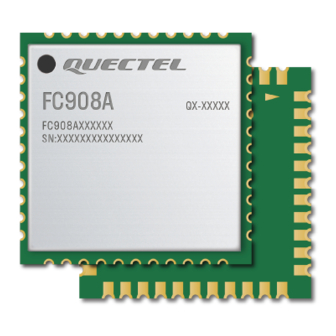
Page 46: Top And Bottom Views
Figure 21: Top and Bottom Views of the Module NOTE Images above are for illustration purpose only and may differ from the actual module. For authentic appearance and label, refer to the module received from Quectel. FC908A_Hardware_Design 45 / 49... -
Page 47: Storage, Manufacturing & Packaging
Wi-Fi&Bluetooth Module Series Storage, Manufacturing & Packaging 6.1. Storage Conditions The module is provided with vacuum-sealed packaging. MSL of the module is rated as 3. The storage requirements are shown below. 1. Recommended Storage Condition: The temperature shall be 23 ± 5 ° C and the relative humidity shall be 35–60 %. -
Page 48: Manufacturing And Soldering
Wi-Fi&Bluetooth Module Series NOTE 1. To avoid blistering, layer separation and other soldering issues, extended exposure of the module to the air is forbidden. 2. Take out the module from the package and put it on high-temperature-resistant fixtures before baking. All modules must be soldered to PCB within 24 hours after the baking, otherwise put them in the drying oven. - Page 49 4. Avoid using ultrasonic technology for module cleaning since it can damage crystals inside the module. 5. Due to the complexity of the SMT process, please contact Quectel Technical Supports in advance for any situation that you are not sure about, or any process (e.g. selective soldering, ultrasonic soldering) that is not mentioned in document [3].
-
Page 50: Packaging Specifications
Wi-Fi&Bluetooth Module Series 6.3. Packaging Specifications The module adopts carrier tape packaging and details are as follow: 6.3.1. Carrier Tape Dimension details are as follow: Figure 23: Carrier Tape Dimension Drawing Table 35: Carrier Tape Dimension Table (Unit: mm) 0.35 12.4 12.4 11.5... -
Page 51: Packaging Process
Wi-Fi&Bluetooth Module Series Table 36: Plastic Reel Dimension Table (Unit: mm) øD1 øD2 24.5 6.3.3. Packaging Process Place the module into the carrier tape and use the cover tape to cover it; then wind the heat-sealed carrier tape to the plastic reel and use the protective tape for protection. -
Page 52: Appendix References
Wi-Fi&Bluetooth Module Series Appendix References Table 37: Related Documents Document Name Quectel_UMTS<E_EVB_User_Guide Quectel_RF_Layout_Application_Note Quectel_Module_Secondary_SMT_Application_Note Table 38: Terms and Abbreviations Abbreviation Description Access Point Bluetooth Low Energy BPSK Binary Phase Shift Keying Bluetooth Complementary Code Keying Clear To Send DQPSK Differential Quadrature Reference Phase Shift Keying GATT Generic Attribute Profile Ground... - Page 53 Wi-Fi&Bluetooth Module Series Mbps Million Bits Per Second Quadrature Amplitude Modulation QPSK Quadrature Phase Shift Keying Radio Frequency RoHS Restriction of Hazardous Substances Spike-triggered average Request to Send Receive Data To Be Determined Transmit Data UART Universal Asynchronous Receiver/Transmitter Universal Serial Bus Maximum High-level Input Voltage Minimum High-level Input Voltage Maximum Low-level Input Voltage...
Need help?
Do you have a question about the FC908A and is the answer not in the manual?
Questions and answers