
Subscribe to Our Youtube Channel
Related Manuals for Phytec L-827e.A3 phyCORE-i.MX 6UL/ULL


Summary of Contents for Phytec L-827e.A3 phyCORE-i.MX 6UL/ULL
- Page 1 L-827e.A3 phyCORE-i.MX 6UL/ULL Hardware Manual A product of PHYTEC Technology Holding Company...
- Page 2 L-827e.A3 phyCORE-i.MX 6UL/ULL Hardware Manual L-827e.A3 phyCORE-i.Mx 6UL/ULL Hardware Manual Document Title L-827e.A3 phyCORE-i.Mx 6UL/ULL Hardware Manual Article Number L-827e.A3 Release Date 18.07.2022 SOM Prod. No. PCM-063 SOM PCB No. 1468.x © PHYTEC Messtecknik GmbH...
- Page 3 L-827e.A3 phyCORE-i.MX 6UL/ULL Hardware Manual © PHYTEC Messtecknik GmbH...
-
Page 4: Ordering Information
Production-ready Board Support Packages (BSPs) and Design Services for our hardware will further reduce your development time and risk and allow you to focus on your product expertise. Take advantage of Phytec products to shorten time-to-market, reduce development costs, and avoid substantial design issues and risks. With this new innovative full system solution, you will be able to bring your new ideas to market in the most timely and cost- efficient manner. - Page 5 Populated on the SOM / SBC With the purchase of a PHYTEC SOM / SBC you will, in addition to our hardware and software possibilities, receive free obsolescence maintenance service for the hardware we provide. Our PCM (Product Change Management) team of developers is continuously processing all incoming PCNs (Product Change Notifications) from vendors and distributors concerning parts that are used in our products.
- Page 6 1.5 PHYTEC Documentation PHYTEC will provide a variety of hardware and software documentation for all of our products. This includes any or all of the following: •...
- Page 7 L-827e.A3 phyCORE-i.MX 6UL/ULL Hardware Manual On top of these standard manuals and guides, PHYTEC will also provide Product Change Notifications, Application Notes, and Technical Notes. These will be done on a case-by-case basis. Most of the documentation can be found in the applicable download page of our products.
-
Page 8: Conventions, Abbreviations, And Acronyms
L-827e.A3 phyCORE-i.MX 6UL/ULL Hardware Manual 2 Conventions, Abbreviations, and Acronyms ® This hardware manual describes the PCM-063 System on Module in the following referred to as phyCORE -i.MX 6UL/ ® ULL. The manual specifies the phyCORE -i.MX 6UL/ULL's design and function. Precise specifications for the NXP®... - Page 9 L-827e.A3 phyCORE-i.MX 6UL/ULL Hardware Manual 2.2 Types of Signals Different types of signals are brought out at the phyCORE-Connector. The following table lists the abbreviations used to specify the type of a signal. TABLE 1: Signal Types used in this Manual...
- Page 10 L-827e.A3 phyCORE-i.MX 6UL/ULL Hardware Manual PCIe Output Differential line pairs 100 Ohm PCIe level output PCIe_O MIPI CSI‑2 Input Differential line pairs 100 Ohm MIPI CSI‑2 level input CSI‑2_I © PHYTEC Messtecknik GmbH...
-
Page 11: Abbreviations And Acronyms
Solder jumpers; these types of jumpers require solder equipment to remove and place Solderless jumpers; these types of jumpers can be removed and placed by hand with no special tools Printed circuit board PHYTEC Display Interface; defined to connect PHYTEC display adapter boards, or custom adapters PHYTEC Extension Board PMIC... - Page 12 L-827e.A3 phyCORE-i.MX 6UL/ULL Hardware Manual Abbreviation Definition Power-on reset Real-time clock Surface mount technology ® System on Module; used in reference to the PCL-063 / phyCORE ‑i.MX 6UL/ULL module User button Sx (e.g. S1, S2, etc.) used in reference to the available user buttons, or DIP-Switches...
- Page 13 The phyCORE‑i.MX 6UL/ULL belongs to Phytec’s phyCORE System on Module family. The phyCORE SOMs represent the continuous development of the PHYTEC System on Module technology. Like its mini-, micro-, and nanoMODUL predecessors, the phyCORE boards integrate all core elements of a microcontroller system on a subminiature board and are designed in a manner that ensures their easy expansion and embedding in peripheral hardware developments.
- Page 14 1. The maximum memory size listed is as of the printing of this manual. Please contact PHYTEC for more information about additional, or new module configurations available. 2. The JTAG pins are used for other functions (SAI2 interface and SPDIF) within the included BSP.
-
Page 15: Block Diagram
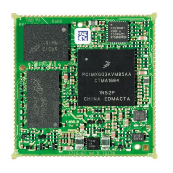
L-827e.A3 phyCORE-i.MX 6UL/ULL Hardware Manual 3.2 Block Diagram FIGURE 1: Block Diagram of the phyCORE‑i.MX 6UL/ULL Note The specified direction indicated refers to the standard phyCORE use of the pin. © PHYTEC Messtecknik GmbH... - Page 16 L-827e.A3 phyCORE-i.MX 6UL/ULL Hardware Manual 3.3 phyCORE-i.MX 6UL/ULL Component Placement FIGURE 2: phyCORE‑i.MX 6UL/ULL Component Placement (top view) © PHYTEC Messtecknik GmbH...
- Page 17 L-827e.A3 phyCORE-i.MX 6UL/ULL Hardware Manual FIGURE 3: phyCORE‑i.MX 6UL/ULL Component Placement (bottom view) © PHYTEC Messtecknik GmbH...
- Page 18 L-827e.A3 phyCORE-i.MX 6UL/ULL Hardware Manual 3.4 Minimum Requirements to Operate the phyCORE-i.MX 6UL/ULL The basic operation of the phyCORE‑i.MX 6UL/ULL only requires a supply of a +3.3 V input voltage and the corresponding GND connection. For information about the power consumption please refer to...
-
Page 19: Pin Description
L-827e.A3 phyCORE-i.MX 6UL/ULL Hardware Manual 4 Pin Description Please note that all module connections are not to exceed their expressed maximum voltage or current. Maximum signal input values are indicated in the corresponding controller manuals/datasheets. As damage from improper connections varies according to use and application, it is the user's responsibility to take appropriate safety measures to ensure that the module connections are protected from overloading through connected peripherals. - Page 20 L-827e.A3 phyCORE-i.MX 6UL/ULL Hardware Manual FIGURE 4: Pinout of the phyCORE-Connector (top view) Warning There was a change in the pin assignment in a former PCB revision as can be seen below. Only use the new pin-assignment corresponding to PCB-No. 1468.1 for your baseboard designs. For more information please refer to the product change notification LPN-228e_2.
- Page 21 L-827e.A3 phyCORE-i.MX 6UL/ULL Hardware Manual Warning The NXP® Semiconductor i.MX 6UL/ULL is a multi-voltage operated microcontroller and as such special attention should be paid to the interface voltage levels to avoid unintentional damage to the microcontroller and other on-board components. Please refer to the NXP Semiconductor i.MX 6UL/ULL Reference Manual for details on the functions and features of controller signals and port pins.
- Page 22 L-827e.A3 phyCORE-i.MX 6UL/ULL Hardware Manual TABLE 4: Pinout of the phyCORE-Connector (Side 1) Pin # Signal (pad name) Voltage domain Description 1. side Ground 0 V X_CSI_VSYNC VDD_3V3 CSI vertical sync. X_CSI_HSYNC VDD_3V3 CSI horizontal sync. X_CSI_PIXCLK VDD_3V3 CSI pixel clock...
- Page 23 L-827e.A3 phyCORE-i.MX 6UL/ULL Hardware Manual X_LCD_ENABLE VDD_3V3 LCD enable X_LCD_CLK VDD_3V3 LCD clock X_LCD_VSYNC VDD_3V3 LCD vertical sync. X_LCD_RESET VDD_3V3 LCD reset X_LCD_HSYNC VDD_3V3 LCD horizontal sync. X_LCD_D0 VDD_3V3 LCD data 0 X_LCD_D1 VDD_3V3 LCD data 1 X_LCD_D2 VDD_3V3 LCD data2...
- Page 24 L-827e.A3 phyCORE-i.MX 6UL/ULL Hardware Manual TABLE 5: Pinout of the phyCORE-Connector (Side 2) Pin # Signal (pad name) Voltage Description domain 2. side Ground 0 V X_LCD_D7 VDD_3V3 LCD data7 X_LCD_D8 VDD_3V3 LCD data8 X_LCD_D9 VDD_3V3 LCD data9 X_LCD_D10 VDD_3V3 LCD data 10...
- Page 25 L-827e.A3 phyCORE-i.MX 6UL/ULL Hardware Manual X_LCD_D23 VDD_3V3 uSDHC2 data 3, LCD data 23 X_CSI_FIELD VDD_3V3 CSI field / camera control X_GPIO5_9 VDD_SNVS GPIO5_9 X_ENET2_TX_D0 VDD_3V3 ETH2 RMII transmit data 0 X_ENET2_TX_D1 VDD_3V3 ETH2 RMII transmit data 1 X_ENET2_TX_EN VDD_3V3 ETH2 RMII transmit enable...
- Page 26 L-827e.A3 phyCORE-i.MX 6UL/ULL Hardware Manual TABLE 6: Pinout of the phyCORE-Connector (Side 3) Pin # Signal (pad name) Voltage Description domain Side 3 X_UART5_TX VDD_3V3 UART5 serial data transmit X_UART5_RX VDD_3V3 UART5 serial data receive X_USB_OTG1_D- USB_I/ i.MX 6UL USB OTG1 data-...
- Page 27 L-827e.A3 phyCORE-i.MX 6UL/ULL Hardware Manual X_JTAG_TDI/ VDD_3V3 SAI2 transmit bit clock SAI2_TX_BCLK X_JTAG_TCK/SAI2_RXD VDD_3V3 SAI2 receive data X_JTAG_MOD VDD_3V3 SPDIF output line signal X_JTAG_TDO/ VDD_3V3 SAI2 transmit frame sync SAI2_TX_SYNC X_JTAG_TMS/SAI2_MCLK VDD_3V3 SAI2 master clock X_nJTAG_TRST_B/ VDD_3V3 SAI2 transmit data...
- Page 28 L-827e.A3 phyCORE-i.MX 6UL/ULL Hardware Manual TABLE 7: Pinout of the phyCORE-Connector (Side 4) Pin # Signal (pad name) Voltage Description domain Side 4 VDD_SNVS PWR_ 3.3 V Backup voltage supply input X_GPIO5_5 VDD_3V3 GPIO5_5 X_GPIO1_1 VDD_3V3 GPIO1_1 X_USB_OTG1_ID VDD_3V3 USB OTG1 ID pin...
- Page 29 L-827e.A3 phyCORE-i.MX 6UL/ULL Hardware Manual X_ECSPI3_MISO VDD_3V3 ECSPI3 master input / slave output X_FLEXCAN1_RX VDD_3V3 FLEXCAN1 receive X_FLEXCAN1_TX VDD_3V3 FLEXCAN1 transmit X_CSI_D0 VDD_3V3 CSI data 0 X_CSI_D1 VDD_3V3 CSI data 1 X_CSI_D2 VDD_3V3 CSI data 2 X_CSI_D3 VDD_3V3 CSI data 3...
- Page 30 L-827e.A3 phyCORE-i.MX 6UL/ULL Hardware Manual TABLE 8: Pinout of the phyCORE-Connector (Pads) Pin # Signal (pad name) Voltage Description domain Pads on the bottom side Ground 0 V Ground 0 V Ground 0 V Ground 0 V Ground 0 V Ground 0 V Ground 0 V Ground 0 V Ground 0 V...
- Page 31 L-827e.A3 phyCORE-i.MX 6UL/ULL Hardware Manual Ground 0 V Ground 0 V Ground 0 V Ground 0 V Ground 0 V Ground 0 V Ground 0 V Ground 0 V Ground 0 V Ground 0 V Ground 0 V Ground 0 V Ground 0 V Ground 0 V Ground 0 V Ground 0 V 4. The specified direction indicated refers to the pins' use according to the phyCORE‑i.MX 6UL/ULL specification.
- Page 32 L-827e.A3 phyCORE-i.MX 6UL/ULL Hardware Manual 5 Jumpers For configuration purposes, the phyCORE‑i.MX 6UL/ULL has several solder jumpers, some of which have been installed prior to delivery. Typical Jumper Pad Numbering Scheme illustrates the numbering of the solder jumper pads, while Jumper Locations (top view) indicates the location and the default configuration of the solder jumpers on the board.
- Page 33 L-827e.A3 phyCORE-i.MX 6UL/ULL Hardware Manual FIGURE 6: Jumper Locations (top view) Please pay special attention to the “TYPE” column to ensure you are using the correct type of jumper (0 Ohms, 10k Ohms, etc…). The jumpers are 0402 packages with a 1/8 W or better power rating. The jumpers (J = solder jumper) have the following functions: ©...
- Page 34 L-827e.A3 phyCORE-i.MX 6UL/ULL Hardware Manual TABLE 9: Jumper Settings Jump Description Type Secti J10 configures the chip to enable signal E1 of the serial memory at U3. In the high- nibble of the address, I C memory devices have the slave ID 0x5. The low nibble of...
- Page 35 L-827e.A3 phyCORE-i.MX 6UL/ULL Hardware Manual 6 Power The phyCORE‑i.MX 6UL/ULL operates off of a single power supply voltage. The following sections discuss the primary power pins on the phyCORE‑Connector X1 in detail. 6.1 Primary System Power (VDD_3V3) The phyCORE‑i.MX 6UL/ULL operates off of primary voltage supply with a nominal value of +3.3 V. On-board switching regulators generate the DDR3L voltage 1.35 V and the core voltage 1.4 V which is switchable to 1.3 V or...
-
Page 36: Power Domains
L-827e.A3 phyCORE-i.MX 6UL/ULL Hardware Manual The above values are to be seen as an orientation for dimensioning the power supply of the SOM. In order to ensure the proper functionality of the SOM, we recommend that the power supply is design to provide approximately 20 % higher currents. - Page 37 L-827e.A3 phyCORE-i.MX 6UL/ULL Hardware Manual 6.4 Switching Supply Voltages for External Logic The phyCORE’s logic circuitry is directly supplied from the module's main input voltage VDD_3V3 (3.3 V). If the external components on a customer baseboard are supplied with the same 3.3 V source as the module, there is no need for special power-up or power-down sequences.
- Page 38 L-827e.A3 phyCORE-i.MX 6UL/ULL Hardware Manual 7 Reset Pin 98 at X1 on the phyCORE‑Connector is designated as reset output. Pin 100 at X1 on the phyCORE‑Connector is designated as a reset input. The reset input signal X_nRESET_IN is connected to the voltage supervisor U5 on the phyCORE module. This device monitors the VDD_3V3 input voltage and reacts to other reset triggers, e.g.
-
Page 39: System Configuration And Booting
L-827e.A3 phyCORE-i.MX 6UL/ULL Hardware Manual 8 System Configuration and Booting Although most features of the i.MX 6UL/ULL microcontroller are configured and/or programmed during the initialization routine, other features, which impact program execution, must be configured prior to initialization via pin termination. - Page 40 L-827e.A3 phyCORE-i.MX 6UL/ULL Hardware Manual 8.2 Boot Device Selection and Configuration In normal operation (boot mode 0, or 2), the boot ROM uses the state of BOOT_MODE and eFUSEs to determine the boot device. During development, it is advisable to set the boot type to “Internal boot” (BOOT_MODE[1:0]=1012 to allow choosing and configuring the boot device by using GPIO pin inputs.
- Page 41 L-827e.A3 phyCORE-i.MX 6UL/ULL Hardware Manual TABLE 12: Boot Configuration Pins at the phyCORE‑Connector Configuration Pin Pin # Signal Description BCFG1[0] X_LCD_D0 3.3 V LCD_DATA_00 BCFG1[1] X_LCD_D1 3.3 V LCD_DATA_01 BCFG1[2] X_LCD_D2 3.3 V LCD_DATA_02 BCFG1[3] X_LCD_D3 3.3 V LCD_DATA_03 BCFG1[4] X_LCD_D4 3.3 V LCD_DATA_04 BCFG1[5] X_LCD_D5 3.3 V...
- Page 42 00000000 00000000 address bytes) eMMC (usdhc 2 interface) 01100000 01001000 00000000 SD-Card (usdhc 1 interface) 01000010 00100000 00000000 10. For series production, PHYTEC offers to order the phyCORE‑i.MX 6UL/ULL with a custom configuration of the eFUSEs © PHYTEC Messtecknik GmbH...
-
Page 43: System Memory
The following sections detail each memory type used on the phyCORE‑i.MX 6UL/ULL. 1. The maximum memory size listed is as of the printing of this manual. Please contact PHYTEC for more information about additional, or new module configurations available. 9.1 DDR3-SDRAM (U6) The RAM memory of the phyCORE‑i.MX 6UL/ULL is comprised of one 16-bit wide DDR3-SDRAM chip (U6). - Page 44 L-827e.A3 phyCORE-i.MX 6UL/ULL Hardware Manual Write protection to the device is accomplished by a high level on signal Write Control when resistor R102 is removed. If resistor R101 is mounted write protection can also be changed by the EEPROM_WP signal [12] (GPIO5_06).
- Page 45 L-827e.A3 phyCORE-i.MX 6UL/ULL Hardware Manual 10 SD/MM Card Interfaces The phyCORE bus features two SD / MM Card interfaces. On the phyCORE‑i.MX 6UL/ULL the interface signals extend from the controllers first and second Ultra Secured Digital (uSDHC1 / uSDHC2) Host Controller to the phyCORE- Connector.
- Page 46 L-827e.A3 phyCORE-i.MX 6UL/ULL Hardware Manual X_LCD_D15 VDD_3V3 [13] uSDHC2 data 5 [13] X_LCD_D16 VDD_3V3 uSDHC2 data 6 [13] X_LCD_D17 VDD_3V3 uSDHC2 data 7 The interfaces do not provide dedicated card-detect or write-protect signals. The card-detect and write-protect function can be implemented easily by using GPIOs of the i.MX 6UL/ULL.
-
Page 47: Serial Interfaces
L-827e.A3 phyCORE-i.MX 6UL/ULL Hardware Manual 11 Serial Interfaces The phyCORE‑i.MX 6UL/ULL provides numerous dedicated serial interfaces some of which are equipped with a transceiver to allow direct connection to external devices: 2x High-speed UARTs (TTL, derived from UART1 and UART5 of the i.MX 6UL/ULL) with up to 4 MHz and one with hardware flow control (RTS and CTS signals) 2x High-speed USB OTG/host interfaces (extended directly from the i.MX 6UL/ULL’s USB PHY (USBPHY1,... - Page 48 L-827e.A3 phyCORE-i.MX 6UL/ULL Hardware Manual X_UART5_CTS_B VDD_3V3 UART5 serial clear to send output (low active, usually used as RTS) X_UART5_RTS_B VDD_3V3 UART5 serial request to send input (low active, usually used as CTS) 11.2 USB OTG/Host Interfaces The phyCORE‑i.MX 6UL/ULL provides two high-speed USB OTG/host interfaces that use the i.MX 6UL/ULL embedded HS USB PHY.
-
Page 49: Ethernet Interface
L-827e.A3 phyCORE-i.MX 6UL/ULL Hardware Manual 11.3 Ethernet Interface Connection of the phyCORE‑i.MX 6UL/ULL to the world wide web or a local area network (LAN) is possible using the onboard Ethernet PHY at U2. It is connected to the RMII interface of the i.MX 6UL/ULL. The PHY operates with a data transmission speed of 10 Mbit/s or 100 Mbit/s. The second Ethernet interface of the i.MX 6UL/ULL is available as an... - Page 50 MAC address. In order to guarantee that the MAC address is unique, all addresses are managed in a central location. Phytec has acquired a pool of MAC addresses. The MAC address of the phyCORE‑i.MX 6UL/ULL is located on the bar code sticker attached to the module.
- Page 51 L-827e.A3 phyCORE-i.MX 6UL/ULL Hardware Manual phyCORE‑Connector X1. The SPI interface provides one chip select signal. The Enhanced Configurable SPI (eCSPI) of the i.MX 6UL/ULL has up to four separate modules (eCSPI1, eCSPI2, eCSPI3 and eCSPI4) which support data rates of up to 52 Mbit/s.
-
Page 52: Audio Interfaces
L-827e.A3 phyCORE-i.MX 6UL/ULL Hardware Manual TABLE 22: I2C Interface Signal Location Pin # Signal Voltage Domain Description X_I2C1_SCL VDD_3V3 I2C1 clock X_I2C1_SDA VDD_3V3 I2C1 data 11.6 Audio Interfaces 11.6.1 I S (SAI) The Synchronous Audio Interface (SAI) of the phyCORE‑i.MX 6UL/ULL is a full-duplex, serial interface that allows... -
Page 53: Can Interface
L-827e.A3 phyCORE-i.MX 6UL/ULL Hardware Manual 11.6.2 SPDIF The Sony/Philips Digital Interface (SPDIF) audio block is a stereo transceiver that allows the processor to receive and transmit digital audio. The following table shows the location of the SPDIF output signal on the phyCORE‑Connector. -
Page 54: General Purpose I/Os
L-827e.A3 phyCORE-i.MX 6UL/ULL Hardware Manual 12 General Purpose I/Os The table below lists all pins not used by any other of the interfaces described explicitly in this manual and which therefore can be used as GPIO without harming other features of the phyCORE‑i.MX 6UL/ULL. - Page 55 L-827e.A3 phyCORE-i.MX 6UL/ULL Hardware Manual 13 User LED [14] The phyCORE‑i.MX 6UL/ULL provides one green user LED (D2) on board . It can be controlled by setting GPIO5_4 to the desired output level. A high-level turns the LED on, a low-level turns it off.
-
Page 56: Debug Interface
L-827e.A3 phyCORE-i.MX 6UL/ULL Hardware Manual 14 Debug Interface The phyCORE‑i.MX 6UL/ULL is equipped with a JTAG interface for downloading program code into the external flash, internal controller RAM, or for debugging programs currently executing. Note On the phyCORE-i.MX 6UL/ULL the JTAG pins are used for other functions (SAI2 interface and SPDIF) within the included BSP. - Page 57 L-827e.A3 phyCORE-i.MX 6UL/ULL Hardware Manual 15 RTC The i.MX 6UL processor also includes an integrated RTC. By default, the RTC is sourced by the internal 32 kHz oscillator. To get a higher accuracy it is possible to connect an external crystal or oscillator (with 32 kHz or 32.768 kHz) to the phyCORE-i.MX 6UL SOM.
-
Page 58: Parallel Display Interface
L-827e.A3 phyCORE-i.MX 6UL/ULL Hardware Manual 16 Display Interface 16.1 Parallel Display Interface The signals from the LCD interface of the i.MX 6UL/ULL are brought out at the phyCORE‑Connector X1. Thus an LCD display with up to 24-bit bus width can be connected directly to the phyCORE‑i.MX 6UL/ULL. The table below shows the location of the applicable interface signals. - Page 59 L-827e.A3 phyCORE-i.MX 6UL/ULL Hardware Manual X_LCD_D11 VDD_3V3 LCD data 11 X_LCD_D12 VDD_3V3 LCD data 12 X_LCD_D13 VDD_3V3 LCD data 13 X_LCD_D14 VDD_3V3 LCD data 14 X_LCD_D15 VDD_3V3 LCD data 15 X_LCD_D16 VDD_3V3 LCD data 16 X_LCD_D17 VDD_3V3 LCD data 17...
-
Page 60: Camera Interfaces
CMOS Sensor Interface (CSI) are available together with an I C interface at the phyCORE‑Connector to allow for camera connectivity according to PHYTEC's phyCAM‑S+, or phyCAM‑P standard. FIGURE 8: Camera Connectivity of the i.MX 6UL/ULL (Y2, G2, and G3) On the phyCORE-i.MX 6UL/ULL SOM CMOS Serial Interface is brought out as parallel interfaces with 10 data bits, HSYNC, VSYNC, MCLK, and PIXCLK. - Page 61 L-827e.A3 phyCORE-i.MX 6UL/ULL Hardware Manual 17.1 Parallel Camera Interface (CSI) The camera parallel interface CSI is available at the phyCORE‑Connector with 10 data bits, HSYNC, VSYNC, MCLK, PIXCLK, and I²C Bus. The following table shows the location of the parallel CSI camera signals at the phyCORE‑Connector.
- Page 62 17.2 Utilizing the Camera Interfaces on a Carrier Board On PHYTEC carrier boards the interface is used directly as a parallel interface according to the phyCAM-P standard. On the target application board, it is also possible to convert the signals with an LVDS deserializer as a serial interface following the phyCAM‑S+ standard.
-
Page 63: Tamper Detection
L-827e.A3 phyCORE-i.MX 6UL/ULL Hardware Manual 18 Tamper Detection The phyCORE-i.MX 6UL/ULL supports the tamper detection feature of the i.MX 6UL processor version G3. With the tamper detection feature, it is possible to recognize when the device encounters unauthorized opening or tampering. -
Page 64: Technical Specifications
L-827e.A3 phyCORE-i.MX 6UL/ULL Hardware Manual 19 Technical Specifications FIGURE 12: Physical Dimensions (bottom view) The physical dimensions of the square phyCORE‑i.MX 6UL/ULL are represented above. The module’s profile is max. 2.9 mm thick, with a maximum component height of 1.2 mm (microcontroller) on the top side of the PCB. The board itself can be easily soldered directly onto your carrier board. - Page 65 L-827e.A3 phyCORE-i.MX 6UL/ULL Hardware Manual Humidity: 95 % r.F. not condensed Operating voltage: VCC 3.3 V +/- 5 % Power consumption: Linux prompt only: typical 0.5 W Full load: typical 1 W Conditions: 512 MB DDR3-SDRAM, 512 MB NAND Flash, Ethernet, G2 528 MHz CPU frequency, 20 °C, 3.3 V These specifications describe the standard configuration of the phyCORE‑i.MX 6UL/ULL as of the printing of this...
- Page 66 L-827e.A3 phyCORE-i.MX 6UL/ULL Hardware Manual TABLE 34: Product Temperature Grades Product Controller Temp Range (Junction Temp) RAM (Case Others Temp. Temp) (Ambient) Grade Industrial -40 °C to +105 °C / Automotive -40 °C Industrial Industrial to+125 °C -40 °C to +95 °C -40 °C to +85 °C Extended Commercial...
- Page 67 L-827e.A3 phyCORE-i.MX 6UL/ULL Hardware Manual Note To facilitate the integration of the phyCORE‑i.MX 6UL/ULL into your design, the footprint of the phyCORE‑i.MX 6UL/ULL is available for download (Integrating the phyCORE-i.MX 6UL/ULL). © PHYTEC Messtecknik GmbH...
- Page 68 L-827e.A3 phyCORE-i.MX 6UL/ULL Hardware Manual 20 Hints for Integrating and Handling the phyCORE-i.MX 6UL/ULL 20.1 Integrating the phyCORE-i.MX 6UL/ULL 20.1.1 Design Rules Successful integration in user target circuitry greatly depends on the adherence to the layout design rules for the GND connections of the phyCORE module.
-
Page 69: Revision History
L-827e.A3 phyCORE-i.MX 6UL/ULL Hardware Manual 21 Revision History Date Version Changes in this Manual 25.01.2017 Manual First edition. L-827e_1 Describes the phyCORE‑i.MX 6UL/ULL PCB‑Version 1468.0 26.07.2017 Manual Update to PCB-Version 1468.2 L-827e_2 Describing minor changes in pinout and complimenting existing information in depth 18.07.2022...
Need help?
Do you have a question about the L-827e.A3 phyCORE-i.MX 6UL/ULL and is the answer not in the manual?
Questions and answers