
Subscribe to Our Youtube Channel
Related Manuals for Phytec phyCORE i.MX8X


Summary of Contents for Phytec phyCORE i.MX8X
- Page 1 ® phyCORE -i.MX8X Hardware Manual Document No.: L-864e.A1 SOM Prod. No.: PCM-065 SOM PCB. No.: 1488.2 CB Prod. No.: PCM-942 CB PCB. No.: 1491.1 Edition: Feb 2021 A product of a PHYTEC Technology Holding company...
- Page 2 Additionally, PHYTEC offers no guarantee nor accepts any liability for damages arising from the improper usage or improper installation of the hardware or software. PHYTEC further reserves the right to alter the layout and/or design of the hardware without prior notification and accepts no liability for doing so.
-
Page 3: Table Of Contents
Flash ..........................38 NAND ............................39 OSPI .............................. 39 SD/MMC/SDIO ..........................40 System Boot Configuration ........................41 Serial Interfaces ............................ 42 CAN ............................... 42 Ethernet ............................42 C ..............................44 Media Local Bus ..........................45 © PHYTEC America LLC, 2021... - Page 4 11.6 MQS .............................. 59 11.7 Security ............................59 11.8 Tamper ............................60 11.9 Watchdog ............................60 12 Hints for Integrating and Handling the phyCORE-i.MX8X ..............61 12.1 Integration ............................61 12.2 Modification ............................ 61 Revision History............................... 62 © PHYTEC America LLC, 2021...
-
Page 5: List Of Figures
Figure 5. Pinout of the phyCORE-Connector (top view, with cross section insert) .......... 28 Figure 6. Jumper Locations (Top Side) ......................25 Figure 7. Jumper Locations (Underside) ......................26 Figure 8. Power Management Diagram ......................37 © PHYTEC America LLC, 2021... -
Page 6: List Of Tables
Table 44. Parallel Camera Connections at the phyCORE-Connector ............. 54 Table 45. ADC Connections at the phyCORE-Connector ................55 Table 46. FlexTimer Signals ........................... 55 Table 47. Total Available GPIO ........................55 Table 48. GPIO0 Accessibility at phyCORE-Connector .................. 56 © PHYTEC America LLC, 2021... - Page 7 Table 55. KPP Signals ............................ 59 Table 56. MQS Signals ..........................59 Table 57. Security Signals ..........................59 Table 58. Tamper Signals ..........................60 Table 59. Watchdog Signals ........................... 60 Table 60. Document Revision History ......................62 © PHYTEC America LLC, 2021...
-
Page 8: Preface
PHYTEC supports a variety of Arm-based and other microprocessors in two ways. 1. As the basis for PHYTEC development kits and Single Board Computers, which serves as a reference and evaluation platform. -
Page 9: Product Change Management
SOMs and SBCs. End users no longer need to redesign entire CPU circuitry and engage in version control to accommodate new or obsolete parts. Instead, PHYTEC manages this at the SOM-level. PHYTEC ensure continued availability of pin- and function-compatible SOMs and SBCs, further minimizing maintenance costs and risks. -
Page 10: Conventions, Abbreviations And Acronyms
Carrier Board; used in reference to the phyCORE Development Kit Carrier Board CMOS Sensor Interface Double data rate DRAM Dynamic random access memory Electromagnetic Compatibility Electromagnetic Interference GPIO General-Purpose Input/Output General-Purpose Timer Solder Jumper: these types of jumpers require solder equipment to remove and place © PHYTEC America LLC, 2021... -
Page 11: Table 2. Signal Types Used In This Manual
Printed circuit board Peripheral Component Interconnect PCIe PCI express Product Change Management Product Change Notification PHYTEC Display Interface; defined to connect PHYTEC display adapter boards, or custom adapters PHYTEC Expansion Board PMIC Power management IC Power-on reset Pulse-width Modulation Real-time clock... - Page 12 PCIe Input Differential line pairs 100 Ohm PCIe level input PCIe_I PCIe Output Differential line pairs 100 Ohm PCIe level output PCIe_O MIPI CSI-2 Input Differential line pairs 100 Ohm MIPI CSI-2 level input CSI-2_I © PHYTEC America LLC, 2021...
-
Page 13: Introduction
L-864e.A1 Introduction The phyCORE-i.MX8X belongs to PHYTEC’s phyCORE System on Module family. Like its mini, micro, and nanoMODUL predecessors, the phyCORE boards integrate all core elements of a microprocessor system on a subminiature board and are designed in a manner that ensures their easy expansion and embedding in peripheral hardware developments. -
Page 14: Som Features
Some of the features listed are not available simultaneously due to the muxing options of the various processor pins. Refer to the i.MX8X Datasheet and Processor Reference Manual for further information on available muxing options. © PHYTEC America LLC, 2021... -
Page 15: Block Diagram
PCM-065/phyCORE-i.MX8X System on Module L-864e.A1 Block Diagram Figure 1. phyCORE-i.MX8X Block Diagram © PHYTEC America LLC, 2021... -
Page 16: Physical Dimensions
(connector) side of the PCB and approximately 2.37mm on the top (microprocessor) side. The PCB is approximately 1.68mm thick, 42mm wide, and 52mm long. For more detailed information please refer to the phyCORE-i.MX8X Dimensional Drawing © PHYTEC America LLC, 2021... -
Page 17: Component Placement Diagram
Component Placement Diagram The phyCORE-i.MX8X component placement diagrams presented in this manual (Figure 2 Figure 3) are for quick reference only. Visit our Hardware Documentation Page for a comprehensive, searchable PDF: Component Placement Diagram – phyCORE-i.MX8X © PHYTEC America LLC, 2021... -
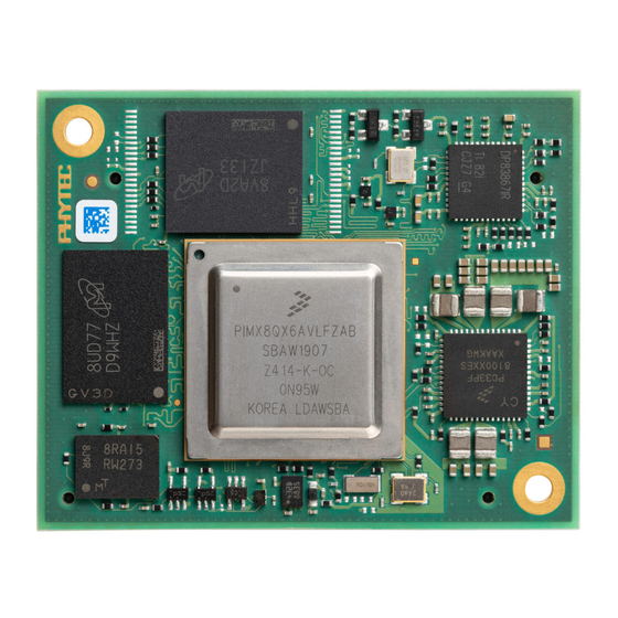
Page 18: Figure 2. Phycore-I.mx8X Component Placement (Processor Side)
PCM-065/phyCORE-i.MX8X System on Module L-864e.A1 Figure 2. phyCORE-i.MX8X Component Placement (Processor Side) © PHYTEC America LLC, 2021... -
Page 19: Figure 3. Phycore-I.mx8X Component Placement (Connector Side)
PCM-065/phyCORE-i.MX8X System on Module L-864e.A1 Figure 3. phyCORE-i.MX8X Component Placement (Connector Side) © PHYTEC America LLC, 2021... -
Page 20: Technical Specifications
Table 3. Technical Specifications Specification Dimensions 52 mm x 42 mm x 4.8 mm Mass ~16.65g Storage Temperature -25C to +85C Operating Temperature -25C to +85C Humidity Typical Idling Power Consumption 1.92W Calculated from idle I Table 4 © PHYTEC America LLC, 2021... -
Page 21: Electrical Specifications
(if programmed to do so by the OTP_VSNVSVOTL[1:0] bits) and is expected to provide power to the SNVS domain on the MCU as long as the LICELL pin has a valid input suitable to supply the configured VSNVS output voltage. The Yes Command © PHYTEC America LLC, 2021... -
Page 22: Minimum Requirements For Operation
Connect all available 3.3V input pins to a power supply on a custom carrier board that provides at least 2000 mA. • At minimum, connect the matching number of ground pins neighboring the 3.3V pins. However, PHYTEC highly recommends connecting all ground pins for proper implementation of the phyCORE-i.MX8X SOM. •... -
Page 23: Solder Jumpers
If soldered jumpers need to be removed, the use of a desoldering pump, desoldering braid, an infrared desoldering station, desoldering tweezers, hot air rework station or other desoldering method is strongly recommended. Follow the instructions carefully for whatever method of removal is used. © PHYTEC America LLC, 2021... -
Page 24: Table 6. Solder Jumper Settings
X_USDHC1_DATA1/NAND_RE_B, X_USDHC1_DATA2/NAND_WE_B, X_USDHC1_DATA3/NAND_ALE Connect VSELECT to X_USDHC1_VSELECT/NAND_RE_P Connect VSELECT to ground Connects LDO2EN pin on the PMIC (U1) to a signal or ground. LDO2EN enables VCC_LDO_SD1. 0 Ohm Connect LDO2EN to X_USDHC1_RESET_B/NAND_RE_N Connect LDO2EN to ground © PHYTEC America LLC, 2021... -
Page 25: Solder Jumper Locations
PCM-065/phyCORE-i.MX8X System on Module L-864e.A1 Solder Jumper Locations Figure 5. Jumper Locations (Processor Side) © PHYTEC America LLC, 2021... -
Page 26: Figure 7. Jumper Locations (Underside)
PCM-065/phyCORE-i.MX8X System on Module L-864e.A1 Figure 6. Jumper Locations (Connector Side) © PHYTEC America LLC, 2021... -
Page 27: Pin Descriptions
This may cause current to flow through the IO pins before the processor is properly powered, potentially resulting in damage or unknown behavior after power-up or reset. Therefore, PHYTEC recommends NOT powering external peripherals and circuits that directly interface with the phyCORE-i.MX8X SOM IOs until their respective voltage domains are powered. -
Page 28: Figure 5. Pinout Of The Phycore-Connector (Top View, With Cross Section Insert)
Manual, or the schematic to learn about alternative functions. In order to utilize a specific pin's alternative function, the corresponding registers must be configured within the appropriate driver of the BSP. Figure 7. Pinout of the phyCORE-Connector (top view, with cross section insert) © PHYTEC America LLC, 2021... -
Page 29: Pinout Tables
SAI1 Receive Data X_SAI1_RXC 3.3V SAI1 Receive Clock X_SAI1_RXFS 3.3V SAI1 Receive Frame Sync Ground X_FLEXCAN0_TX 3.3V FlexCAN0 Transmit Data X_FLEXCAN0_RX 3.3V FlexCAN0 Receive Data X_FLEXCAN1_RX 3.3V FlexCAN1 Receive Data X_FLEXCAN1_TX 3.3V FlexCAN1 Transmit Data Ground © PHYTEC America LLC, 2021... -
Page 30: Table 8. Phycore-I.mx8X Connector X1, Column B Pinout
USB3 Super Speed 3 X_USB3_SS3_TC0 3.3V Transmission Control 0 USB3 Super Speed 3 X_USB3_SS3_TC1 3.3V Transmission Control 1 Ground USB3 Super Speed 3 X_USB3_SS3_TC2 3.3V Transmission Control 2 USB3 Super Speed 3 X_USB3_SS3_TC3 3.3V Transmission Control 3 Ground © PHYTEC America LLC, 2021... - Page 31 Ground X_SPI3_CS0 3.3V SPI3 Chip Select 0 X_SPI3_CS1 3.3V SPI3 Chip Select 1 X_SPI3_SCK 3.3V SPI3 Clock X_SPI3_SDI 3.3V SPI3 Data In X_SPI3_SDO 3.3V SPI3 Data Out Ground X_ETH0_D-/MAC_CLK ETH_I/O Differential Ethernet Data D Negative © PHYTEC America LLC, 2021...
-
Page 32: Table 9. Phycore-I.mx8X Connector X1, Column C Pinout
MIPI DSI1 Data 1 Negative X_MIPI_DSI1_DATA1_P Differential AR17 MIPI DSI1 Data 1 Positive Ground X_MIPI_DSI1_DATA0_N Differential AN15 MIPI DSI1 Data 0 Negative X_MIPI_DSI1_DATA0_P Differential AR15 MIPI DSI1 Data 0 Positive X_MIPI_DSI1_DATA3_N Differential AM18 MIPI DSI1 Data 3 Negative © PHYTEC America LLC, 2021... -
Page 33: Table 10. Phycore-I.mx8X Connector X1, Column D Pinout
AM10 QSPI0 Data 4 X_QSPI0_DATA5 1.8V QSPI0 Data 5 X_QSPI0_DATA6 1.8V AJ11 QSPI0 Data 6 X_QSPI0_DATA7 1.8V QSPI0 Data 7 VCC_OSPI_1V8 PWR_O 1.8V AE15/AE13 VCC OSPI 1.8V Output Ground X_CSI_DO0 3.3V AK28 CSI Data 0 © PHYTEC America LLC, 2021... - Page 34 ADC In 0 Ground X_ADC_IN4 1.8V ADC In 4 X_ADC_IN3 1.8V ADC In 3 X_ADC_IN2 1.8V ADC In 2 X_ADC_IN5 1.8V ADC In 5 Ground PWR_I 3.3V Main Power Supply Input PWR_I 3.3V Main Power Supply Input © PHYTEC America LLC, 2021...
- Page 35 The voltage level for this signal is configurable for 1.8V or 3.3V via J6. The default voltage level is listed here, but always check the actual jumper setting for the applicable SOM configuration. Refer to the Solder Jumpers section for details © PHYTEC America LLC, 2021...
-
Page 36: Power
CAUTION: As a general design rule, PHYTEC recommends connecting all ground pins which are next to signals that are being used in the application circuitry. For maximum EMI performance, all ground pins should be connected to a solid ground plane. -
Page 37: Power Management
I/O should be enabled by the X_PGOOD signal. X_PGOOD is a 3.3V signal that goes high after the SOM has been fully powered up. Use the X_PGOOD signal to sequence your carrier board power supplies and I/O buffers. See Figure 8 below. Figure 8. Power Management Diagram © PHYTEC America LLC, 2021... -
Page 38: System Memory
The default voltage level is listed here, but always check the actual jumper setting for the applicable SOM configuration. Refer to the Solder Jumpers section for details CAUTION: eMMC and NAND cannot be populated at the same time. © PHYTEC America LLC, 2021... -
Page 39: Nand
QSPI0B signals (see the table below) should be changed so that the QSPI1A signals are brought out instead. More information about pin muxing can be found on Hints for Integrating and Handling the phyCORE-i.MX8X under phyCORE-i.MX8X Pin Resources. © PHYTEC America LLC, 2021... -
Page 40: Sd/Mmc/Sdio
The default voltage level is listed here, but always check the actual jumper setting for the applicable SOM configuration. Refer to the Solder Jumpers section for details The voltage level for these signals is configurable between 1.8V and 3.3V via the PMIC LDO2 domain © PHYTEC America LLC, 2021... -
Page 41: System Boot Configuration
To modify the default boot configuration on a custom Carrier Board, it is recommended to use 1k pull-up to VCC_SCU_1V8 (found on pin C47 at the phyCORE-Connector) or pull-down resistors to override the SOM settings. For more information about the boot mode pins, please refer to the i.MX8X Processor Reference Manual. © PHYTEC America LLC, 2021... -
Page 42: Serial Interfaces
LED Link Signal X_ETH0_LED1/MAC_RXD2 3.3V LED Activity Signal SOM Ethernet PHY X_ETH_GPIO0 3.3V GPIO 0 SOM Ethernet PHY X_ETH_GPIO1 3.3V GPIO 1 Ethernet Data A X_ETH0_A-/TX0-/MAC_TXD2 ETH_I/O Differential Negative Ethernet Data A X_ETH0_A+/TX0+/MAC_TXD3 ETH_I/O Differential Positive © PHYTEC America LLC, 2021... -
Page 43: Table 21. Ethernet Phy Default Strapping Configuration
21 below lists the default Ethernet PHY strapping configuration, however these settings can be changed via the register settings of the PHY if necessary. Table 21. Ethernet PHY Default Strapping Configuration Strapping Option Default Setting © PHYTEC America LLC, 2021... -
Page 44: I 2 C
CSI I2C Data Media Local Bus The phyCORE-i.MX8X SOM provides a Media Local Bus interface that provides a link to a MOST® data network, using the standardized MediaLB protocol. It supports a 3-wire interface (MLB25,MLB50). © PHYTEC America LLC, 2021... -
Page 45: Pcie
Table 26. SAI1 Connections at the phyCORE-Connector X1 Pin # Processor Signal SOM Signal Type Level Description Processor Ball SAI1_RXD X_SAI1_RXD 3.3V SAI1 Receive Data SAI1_RXC X_SAI1_RXC 3.3V SAI1 Receive Clock SAI1_RXFS X_SAI1_RXFS 3.3V SAI1 Receive Frame Sync © PHYTEC America LLC, 2021... -
Page 46: Table 27. Sai2 Connections At The Phycore-Connector
ESAI0 Receive Data ESAI0_TX4_RX1 1.8V GMII_TXD0 1/Transmit Data 4 X_ESAI0_TX5_RX0/ENET1_R ESAI0 Receive Data ESAI0_TX5_RX0 1.8V GMII_TXD1 0/Transmit Data 5 ESAI0_RX_HF_C ESAI0 Receive High X_MCLK_IN0 3.3V Frequency Clock ESAI0_TX_HF_C ESAI0 Transmit High X_MCLK_OUT0 3.3V Frequency Clock © PHYTEC America LLC, 2021... -
Page 47: Spdif
CPU. There are six UART modules provided and each can be used for configuration and data exchange with external peripheral devices. SCU UART is dedicated to the SCU and not available for general use. © PHYTEC America LLC, 2021... -
Page 48: Uart
Table 35. USB0 OTG Connections at the phyCORE-Connector X1 Pin # SOM Signal Type Level Processor Ball Description X_USB_OTG1_VBUS USB OTG1 VBUS input X_USB_OTG1_ID 3.3V USB OTG1 2.0 Dual-Role Device Role Select X_USB_OTG1_DP Differential USB OTG1 2.0 Differential Data Positive © PHYTEC America LLC, 2021... -
Page 49: Table 36. Usb1 Otg Connections At The Phycore-Connector
Type Level Processor Ball Description USB_OTG2_VBUS USB OTG2 VBUS input USB OTG2 2.0 Dual-Role Device Role X_USB_OTG2_ID 3.3V Select X_USB_OTG2_DN Differential USB OTG2 2.0 Differential Data Negative X_USB_OTG2_DP Differential USB OTG2 2.0 Differential Data Positive © PHYTEC America LLC, 2021... -
Page 50: Control Interfaces
Table 38. PWM Connections at the phyCORE-Connector Processor Signal SOM Signal Type Level Processor Ball Description X1 Pin # PWM0_OUT X_UART1_TX 3.3V PWM0 PWM1_OUT X_UART1_RX 3.3V PWM1 PWM2_OUT X_UART1_RTS_B 3.3V PWM2 PWM3_OUT X_UART1_CTS_B 3.3V PWM3 © PHYTEC America LLC, 2021... -
Page 51: Debug Interfaces
RAM or for debugging programs currently executing. The UART interface is accessible via the phyCORE-Connector. Table 40. UART Connections at the phyCORE-Connector X1 Pin # SOM Signal Type Level Processor Ball Description X_UART0_TX 1.8V UART0 Transmit Data X_UART0_RX 1.8V UART0 Receive Data © PHYTEC America LLC, 2021... -
Page 52: Display Interfaces
AE33 LVDS1/MIPI DSI1 I2C0 Data X_MIPI_DSI1_I2C0_SDA OD-O 3.3V AC29 LVDS1/MIPI DSI1 I2C0 Clock LVDS1/MIPI DSI1 GPIO 0 (the PWM X_MIPI_DSI1_GPIO0_00 3.3V AD30 is also routed through this signal) X_MIPI_DSI1_GPIO0_01 3.3V AF34 LVDS1/MIPI DSI1 GPIO 1 © PHYTEC America LLC, 2021... -
Page 53: Parallel Lcd Display
LCD Data 23 LCD Horizontal LCD_HSYNC X_SPI0_CS1 1.8V Sync LCD_RESET X_SPI3_CS0 1.8V LCD Reset LCD_EN X_SPI3_CS1 1.8V LCD Enable LCD Vertical LCD_VSYNC X_MCLK_IN1 1.8V Sync LCD_CLK X_MCLK_IN0 1.8V LCD Clock LCD_PWM X_MCLK_OUT0 1.8V LCD PWM © PHYTEC America LLC, 2021... -
Page 54: Camera Interfaces
CSI Data out 7 X_CSI_HSYNC 1.8V AR29 CSI Horizontal Sync X_CSI_VSYNC 1.8V AL27 CSI Vertical Sync X_CSI_EN 1.8V AP28 CSI Enable X_CSI_RESET 1.8V AR27 CSI Reset X_CSI_MCLK 1.8V AM26 CSI Master Clock X_CSI_PCLK 1.8V AK26 CSI Pixel Clock © PHYTEC America LLC, 2021... -
Page 55: Peripheral Interfaces
Many of the GPIOs are multiplexed with other interfaces, some of which connect to on-board circuits. Review the phyCORE-i.MX8X SOM schematic when using these GPIOs to check for pull-up and pull-down resistors, connected devices, etc. © PHYTEC America LLC, 2021... -
Page 56: Table 48. Gpio0 Accessibility At Phycore-Connector
SOM Signal Type Level Processor Ball GPIO1_00 X_SPI2_CS0 1.8V GPIO1_01 X_SPI2_SDO 1.8V GPIO1_02 X_SPI2_SDI 1.8V GPIO1_03 X_SPI2_SCK 1.8V GPIO1_04 X_SPI0_SCK 1.8V GPIO1_05 X_SPI0_SDI 1.8V GPIO1_06 X_SPI0_SDO 1.8V GPIO1_07 X_SPI0_CS1 1.8V GPIO1_08 X_SPI0_CS0 1.8V GPIO1_09 X_ADC_IN1 1.8V © PHYTEC America LLC, 2021... -
Page 57: Table 50. Gpio2 Accessibility At Phycore-Connector
GPIO3_11 X_QSPI0_DATA2 1.8V AJ13 GPIO3_12 X_QSPI0_DATA3 1.8V AH12 GPIO3_13 X_QSPI0A_DQS 1.8V AK10 GPIO3_14 X_QSPI0A_SS0_B 1.8V AM12 GPIO3_15 X_QSPI0A_SS1_B 1.8V AK12 GPIO3_16 X_QSPI0A_SCLK 1.8V AP12 GPIO3_17 X_QSPI0B_SCLK 1.8V AR11 GPIO3_18 X_QSPI0_DATA4 1.8V AM10 GPIO3_19 X_QSPI0_DATA5 1.8V © PHYTEC America LLC, 2021... -
Page 58: Gpt
“set and forget” mode, it can provide precise interrupts at regular intervals with minimal processor intervention. The counter has output compare logic to provide the status and interrupt at comparison. This timer can be configured to run either on an external clock or on an internal clock. © PHYTEC America LLC, 2021... -
Page 59: Kpp
Table 57. Security Signals X1 Pin # SOM Signal Type Level Processor Ball Description X_MIPI_CSI0_I2C0_SCL OD-O 1.8V AP26 I2C Clock X_MIPI_CSI0_I2C0_SDA OD-I/O 1.8V AM24 I2C Data X_MIPI_CSI0_MCLK_OUT 1.8V AN25 Enable signal © PHYTEC America LLC, 2021... -
Page 60: Tamper
ARM core, and a second point evokes an external event on the WDOG line. Table 59. Watchdog Signals X1 Pin # Processor Signal SOM Signal Type Level Processor Ball Description WDOG_OUT X_JTAG_TRST_B 1.8V AB28 Watchdog Output © PHYTEC America LLC, 2021... -
Page 61: Hints For Integrating And Handling The Phycore-I.mx8X
Pin Resources: • PHYTEC recommends the use of NXP's Pin Muxing Tool • The following file is a pin muxing reference for PHYTEC Hardware: PCM- 065_1488.2_pinmux.xlsx • The following file is a pin mux file for importing into NXP's Pin Muxing Tool: MIMX8QX6xxxFZ.mex... -
Page 62: Revision History
Revision History Table 60. Document Revision History Date Version Number Changes in this Manual 2020/05/20 L-864e.A0 Preliminary Release 2021/02/12 L-864e.A1 SOM PCB revision from 1488.1 to 1488.2 2021/03/04 L-864e.A2 Updated hyperlinks and Numerical Chapter Headings © PHYTEC America LLC, 2021...
Need help?
Do you have a question about the phyCORE i.MX8X and is the answer not in the manual?
Questions and answers