Table of Contents
Advertisement
Quick Links
1
Introduction ................................................................................................................................................ 2
2
Setup ......................................................................................................................................................... 2
2.1
Connector Description ..................................................................................................................... 2
2.2
Operation ......................................................................................................................................... 3
3
Board Layout ............................................................................................................................................. 4
4
Schematic .................................................................................................................................................. 8
5
Bill of Materials .......................................................................................................................................... 9
1
BYPASS Settings (J3) ............................................................................................................................... 2
¯¯¯ /MUTE Settings (J4) ........................................................................................................................... 2
2
CD
3
TOP Layer ................................................................................................................................................. 4
4
GND Layer ................................................................................................................................................. 5
5
VCC Layer ................................................................................................................................................. 6
6
BOTTOM Layer ......................................................................................................................................... 7
7
Schematic .................................................................................................................................................. 8
1
Bill of Matierals .......................................................................................................................................... 9
SNVU154 - May 2012
Contents
List of Figures
List of Tables
User's Guide
SNVU154 - May 2012
SD034EVK
SD034EVK
1
Advertisement
Table of Contents

Related Manuals for Texas Instruments SD034EVK


Summary of Contents for Texas Instruments SD034EVK
-
Page 1: Table Of Contents
User’s Guide SNVU154 – May 2012 SD034EVK Contents Introduction ..............................2 Setup ................................. 2 Connector Description ........................2 Operation ............................3 Board Layout ............................. 4 Schematic ..............................8 Bill of Materials ............................9 List of Figures BYPASS Settings (J3) ..........................2 ¯¯¯... -
Page 2: Introduction
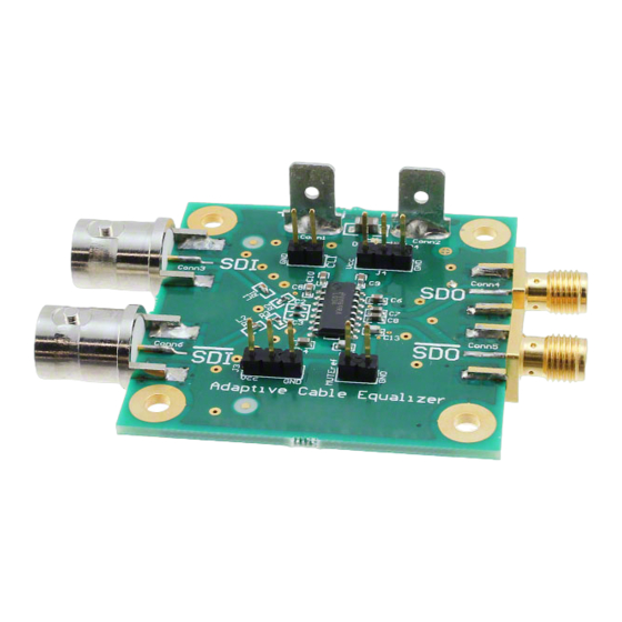
Introduction www.ti.com Introduction The Texas Instruments SD034EVK evaluation kit (EVK) helps designers evaluate the operation and performance of the LMH0034 HD/SD SDI Adaptive Cable Equalizer. Setup This section describes the connectors and jumpers on the board as well as how to properly connect, set up, and use the SD034EVK. -
Page 3: Operation
50Ω SMA cables to Conn4 and Conn5 to observe the differential output, or connect the cable to either Conn4 or Conn5 to view the single-ended output. If only one output is used, the other output should be terminated with a 50Ω SMA termination. SNVU154 – May 2012 SD034EVK... -
Page 4: Board Layout
Board Layout www.ti.com Board Layout The SD034EVK is a 4-layer board (TOP / GND / VCC / BOTTOM). Figure 3, Figure 4, Figure 5, and Figure 6 show the board layout for the SD034EVK. Figure 3: TOP Layer SD034EVK SNVU154 – May 2012... -
Page 5: Gnd Layer
Board Layout Figure 4: GND Layer SNVU154 – May 2012 SD034EVK... -
Page 6: Vcc Layer
Board Layout www.ti.com Figure 5: VCC Layer SD034EVK SNVU154 – May 2012... -
Page 7: Bottom Layer
Board Layout Figure 6: BOTTOM Layer SNVU154 – May 2012 SD034EVK... -
Page 8: Schematic
Schematic www.ti.com Schematic Figure 7: Schematic SD034EVK SNVU154 – May 2012... -
Page 9: Bill Of Materials
3M/ESD 929834-02-36 L1, L2 Inductor, 6.8nH, 0402 VISHAY DALE ILC-0402 6.8NH 5% R1 R2 R3 R5 Yageo America RC0402FR-0775RL Resistor, 75Ω, 0402 Panasonic - ECG ERJ-3GEYJ301V Resistor, 300Ω, 0603 LMH0034 Equalizer, SOIC16 Texas Instruments LMH0034MA SNVU154 – May 2012 SD034EVK... - Page 10 EVALUATION BOARD/KIT IMPORTANT NOTICE Texas Instruments (TI) provides the enclosed product(s) under the following conditions: This evaluation board/kit is intended for use for ENGINEERING DEVELOPMENT, DEMONSTRATION, OR EVALUATION PURPOSES ONLY and is not considered by TI to be a finished end-product fit for general consumer use. Persons handling the product(s) must have electronics training and observe good engineering practice standards.
- Page 11 IMPORTANT NOTICE Texas Instruments Incorporated and its subsidiaries (TI) reserve the right to make corrections, modifications, enhancements, improvements, and other changes to its products and services at any time and to discontinue any product or service without notice. Customers should obtain the latest relevant information before placing orders and should verify that such information is current and complete.
Need help?
Do you have a question about the SD034EVK and is the answer not in the manual?
Questions and answers