Table of Contents
Advertisement
Quick Links
www.ti.com
User's Guide
TPS2640EVM: Evaluation Module for TPS2640
This user's guide describes the evaluation module (EVM) for the Texas instruments TPS2640 devices. The
document provides configuration information and test setup details for working with the EVM. The EVM
schematic, board layout, and bill of materials (BOM) are also included.
1
Introduction.............................................................................................................................................................................2
1.1 EVM Features....................................................................................................................................................................
1.2 EVM Applications...............................................................................................................................................................
2 Description..............................................................................................................................................................................
3
Schematics..............................................................................................................................................................................4
Configurations..........................................................................................................................................................5
4.1 Physical Access.................................................................................................................................................................
4.2 Test Equipment..................................................................................................................................................................
4.3 Test Setup..........................................................................................................................................................................
4.4 Test Procedure...................................................................................................................................................................
Drawings..................................................................................................................................................................16
(BOM).........................................................................................................................................................17
Schematic..........................................................................................................................................4
Setup.........................................................................................................................................................7
Figure 4-2. Output Voltage Start-Up Waveform...........................................................................................................................
Figure 4-3. J5/J12 = 2-3 Position, Current Limit (2.23 A), Auto-Retry Mode.............................................................................
Figure 4-6. J5/J12 = Floating, Current Limit (2.23 A), Circuit Breaker With Auto-Retry Mode..................................................
Figure 4-7. Output Short-Circuit Protection...............................................................................................................................
Figure 4-9. Overvoltage Clamp Response................................................................................................................................
Figure 5-1. Top Side Placement................................................................................................................................................
Layer.................................................................................................................................................................16
Figure 5-3. Bottom Layer...........................................................................................................................................................
Table 4-1. Input and Output Connector Functionality..................................................................................................................
Table 4-2. Test Points Description...............................................................................................................................................
Table 4-3. Jumper and LED Descriptions....................................................................................................................................
Table 4-5. Default Jumper Setting for the TPS2640EVM............................................................................................................
Table 4-6. TPS2640EVM DMM Readings at Different Test Points..............................................................................................
Table 4-8. TPS2640EVM Oscilloscope Setting for the Current Limit Test.................................................................................
Table 4-9. TPS2640EVM Jumper Setting for Current Limits.....................................................................................................
SLVUBX9 - OCTOBER 2020
Submit Document Feedback
ABSTRACT
Table of Contents
Guidelines..................................................................................................16
List of Figures
Mode..................................................................................................................................12
Protection.....................................................................................................................................14
List of Tables
Setting.............................................................................................................................3
TPS2640EVM...............................................................................................................8
Copyright © 2020 Texas Instruments Incorporated
Mode................................................................................11
Test..................................................................9
Test................................................................................................13
TPS2640EVM: Evaluation Module for TPS2640
Table of Contents
2
2
3
5
6
7
8
9
11
12
13
15
16
16
5
5
5
8
8
10
10
1
Advertisement
Table of Contents

Related Manuals for Texas Instruments TPS2640EVM


Summary of Contents for Texas Instruments TPS2640EVM
-
Page 1: Table Of Contents
TPS2640EVM: Evaluation Module for TPS2640 ABSTRACT This user’s guide describes the evaluation module (EVM) for the Texas instruments TPS2640 devices. The document provides configuration information and test setup details for working with the EVM. The EVM schematic, board layout, and bill of materials (BOM) are also included. -
Page 2: Introduction
All other trademarks are the property of their respective owners. 1 Introduction The TPS2640EVM allows reference circuit evaluation of TI's TPS2640 devices. The TPS2640 are compact 4.2- V to 42-V, 2.23-A industrial eFuses with integrated back-to-back FETs, programmable undervoltage, overvoltage, reverse-polarity, overcurrent, inrush current protection, and output current monitoring features. -
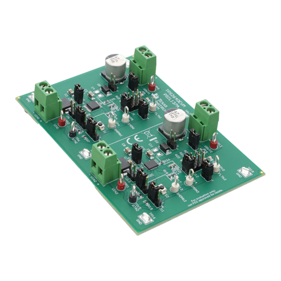
Page 3: Description
Description 2 Description The TPS2640EVM enables full evaluation of the TPS2640 devices. The EVM supports HTSOP and QFN versions of the devices on two channels (CH1 and CH2, respectively). Input power is applied at T1 (CH1) and T3 (CH2) while T2 (CH1) and T4 (CH2) provide an output connection to the load. See the schematic in... -
Page 4: Schematics
3.24k Green PowerPAD 30.1k 402k 22nF TP15 TPS26400RHFR RTN2 RTN2 5.36k 8.06k 12.1k 60.4k TP16 TP17 RTN2 TP18 Figure 3-1. TPS2640EVM Schematic TPS2640EVM: Evaluation Module for TPS2640 SLVUBX9 – OCTOBER 2020 Submit Document Feedback Copyright © 2020 Texas Instruments Incorporated... -
Page 5: General Configurations
General Configurations 4 General Configurations 4.1 Physical Access Table 4-1 lists the TPS2640EVM input and output connector functionality, Table 4-2 describes the test point availability, and Table 4-3 describes the jumper functionality. Table 4-1. Input and Output Connector Functionality... -
Page 6: Test Equipment
A resistive load is recommended for testing. If an electronic load is used, ensure that the output load is set in the constant resistance (CR) mode, not in the constant current (CC) mode. TPS2640EVM: Evaluation Module for TPS2640 SLVUBX9 – OCTOBER 2020 Submit Document Feedback Copyright ©... -
Page 7: Test Setup
General Configurations 4.3 Test Setup Figure 4-1 shows the typical test setup for the TPS2640EVM. Connect T1/T3 to the power supply and T2/T4 to the load. Figure 4-1. EVM Test Setup SLVUBX9 – OCTOBER 2020 TPS2640EVM: Evaluation Module for TPS2640 Submit Document Feedback Copyright ©... -
Page 8: Test Procedure
24 V 24 V 2. Turn on the load and set the load resistance to 16 Ω ±1 Ω. 3. Disable the power supply, load and hook up the TPS2640EVM assembly as shown in Figure 4-1. 4. Make sure the default evaluation board jumper settings are as shown in Table 4-5. -
Page 9: Figure 4-2. Output Voltage Start-Up Waveform
3. Enable the load. 4. Enable the power supply and verify that the output voltage startup waveform is as shown in Figure 4-2. Table 4-7. TPS2640EVM Oscilloscope Setting for the Output Voltage Start-Up Test Oscilloscope Setting CH1 Probe Points CH2 Probe Points... -
Page 10: Table 4-8. Tps2640Evm Oscilloscope Setting For The Current Limit Test
Follow the instructions to verify the current limit and various fault response modes like auto-retry, latch and circuit breaker with auto-retry: 1. Set up the oscilloscope as listed in Table 4-8. Table 4-8. TPS2640EVM Oscilloscope Setting for the Current Limit Test Oscilloscope Setting CH1 Probe Points CH2 Probe Points Channel 1 = 10V / div... -
Page 11: Figure 4-3. J5/J12 = 2-3 Position, Current Limit (2.23 A), Auto-Retry Mode
12.Once the device is latched-off, either the power supply or the SHDNb should be recycled to re-enable it. 13.Change the load resistance to 16 Ω ±1 Ω. SLVUBX9 – OCTOBER 2020 TPS2640EVM: Evaluation Module for TPS2640 Submit Document Feedback Copyright © 2020 Texas Instruments Incorporated... -
Page 12: Figure 4-5. Restart From Latch-Off Mode
18.Enable the power supply and verify the circuit breaker with auto retry fault response waveform as shown in Figure 4-6. Figure 4-6. J5/J12 = Floating, Current Limit (2.23 A), Circuit Breaker With Auto-Retry Mode TPS2640EVM: Evaluation Module for TPS2640 SLVUBX9 – OCTOBER 2020 Submit Document Feedback Copyright © 2020 Texas Instruments Incorporated... -
Page 13: Figure 4-7. Output Short-Circuit Protection
Follow the instructions to verify the output short-circuit protection feature of the device: 1. Set up the oscilloscope as listed in Table 4-10. Table 4-10. TPS2640EVM Output Short-Circuit Protection Test Oscilloscope Setting CH1 Probe Points CH2 Probe Points Channel 1 = 10 V / div... -
Page 14: Figure 4-8. Reverse Polarity Protection
Follow the instructions to verify the reverse polarity protection feature of the device: 1. Set up the oscilloscope as listed in Table 4-11. Table 4-11. TPS2640EVM Reverse Polarity Test Oscilloscope Setting CH1 Probe Points CH2 Probe Points Channel 1 = 10 V / div... -
Page 15: Figure 4-9. Overvoltage Clamp Response
3. Now apply transient input voltage (28 V to 40 V) for 20 ms and verify the Overvoltage clamp response as Figure 4-9 shows. Figure 4-9. Overvoltage Clamp Response SLVUBX9 – OCTOBER 2020 TPS2640EVM: Evaluation Module for TPS2640 Submit Document Feedback Copyright © 2020 Texas Instruments Incorporated... -
Page 16: Evm Board Assembly Drawings And Layout Guidelines
Figure 5-3 show component placement and layout of the EVM. Figure 5-1. Top Side Placement Figure 5-2. Top Layer Figure 5-3. Bottom Layer TPS2640EVM: Evaluation Module for TPS2640 SLVUBX9 – OCTOBER 2020 Submit Document Feedback Copyright © 2020 Texas Instruments Incorporated... -
Page 17: Bill Of Materials (Bom)
Bill Of Materials (BOM) 6 Bill Of Materials (BOM) Table 6-1 displays the EVM BOM. Table 6-1. TPS2640EVM Bill of Materials Designator Value Description Package Reference Part Number Manufacturer Alternate Part Alternate Number Manufacturer !PCB1 Printed Circuit Board PSIL137 C1, C7 0.1uF... - Page 18 Bill Of Materials (BOM) www.ti.com Table 6-1. TPS2640EVM Bill of Materials (continued) Designator Value Description Package Reference Part Number Manufacturer Alternate Part Alternate Number Manufacturer R9, R21 5.36k RES, 5.36 k, 1%, 0.1 W, AEC-Q200 Grade 0603 CRCW06035K36FKEA Vishay-Dale 0, 0603 R10, R22 8.06k...
- Page 19 STANDARD TERMS FOR EVALUATION MODULES Delivery: TI delivers TI evaluation boards, kits, or modules, including any accompanying demonstration software, components, and/or documentation which may be provided together or separately (collectively, an “EVM” or “EVMs”) to the User (“User”) in accordance with the terms set forth herein.
- Page 20 www.ti.com Regulatory Notices: 3.1 United States 3.1.1 Notice applicable to EVMs not FCC-Approved: FCC NOTICE: This kit is designed to allow product developers to evaluate electronic components, circuitry, or software associated with the kit to determine whether to incorporate such items in a finished product and software developers to write software applications for use with the end product.
- Page 21 www.ti.com Concernant les EVMs avec antennes détachables Conformément à la réglementation d'Industrie Canada, le présent émetteur radio peut fonctionner avec une antenne d'un type et d'un gain maximal (ou inférieur) approuvé pour l'émetteur par Industrie Canada. Dans le but de réduire les risques de brouillage radioélectrique à...
- Page 22 www.ti.com EVM Use Restrictions and Warnings: 4.1 EVMS ARE NOT FOR USE IN FUNCTIONAL SAFETY AND/OR SAFETY CRITICAL EVALUATIONS, INCLUDING BUT NOT LIMITED TO EVALUATIONS OF LIFE SUPPORT APPLICATIONS. 4.2 User must read and apply the user guide and other available documentation provided by TI regarding the EVM prior to handling or using the EVM, including without limitation any warning or restriction notices.
- Page 23 Notwithstanding the foregoing, any judgment may be enforced in any United States or foreign court, and TI may seek injunctive relief in any United States or foreign court. Mailing Address: Texas Instruments, Post Office Box 655303, Dallas, Texas 75265 Copyright © 2019, Texas Instruments Incorporated...
- Page 24 TI products. TI’s provision of these resources does not expand or otherwise alter TI’s applicable warranties or warranty disclaimers for TI products. Mailing Address: Texas Instruments, Post Office Box 655303, Dallas, Texas 75265 Copyright © 2020, Texas Instruments Incorporated...
Need help?
Do you have a question about the TPS2640EVM and is the answer not in the manual?
Questions and answers