Advertisement
Quick Links
This user's guide describes the evaluation module (EVM) for the Texas instruments TPS2663x and
TPS1663x eFuse in PWP packages. The document provides EVM configuration information and test
setup details for evaluating the TPS26633 and TPS16630 devices. The EVM schematic, board layout, and
bill of materials (BOM) are also included.
...................................................................................................................
1
Introduction
....................................................................................................................
2
Description
.....................................................................................................................
3
Schematic
4
Connector, Jumper, and LED Descriptions
5
Test Equipment and Setup
6
Test Procedure and Results
7
Board Layout
8
Bill of Materials
9
Evaluating TPS26631 and TPS26636 on TPS2663-166EVM
1
TPS2663-166EVM Schematic
2
TPS2663-166 EVM Setup
3
TPS2663-166EVM Startup for CH1 (V
4
TPS2663-166EVM Startup for CH2 (V
5
TPS2663-166EVM Current Limit Operation for CH1 (V
6
TPS2663-166EVM Current Limit Operation for CH2 (V
7
TPS2663-166EVM Output Hot Short for CH1 (V
8
TPS2663-166EVM Output Hot Short for CH2 (V
9
TPS2663-166EVM Reverse Input Polarity for CH1 (V
10
TPS2663-166EVM Reverse Current Blocking for CH1 (V
11
TPS2663-166EVM Overvoltage Clamping for CH1 (V
12
TPS2663-166EVM Top Overlay
13
TPS2663-166EVM Bottom Overlay
14
TPS2663-166EVM Top Layer
15
TPS2663-166EVM Bottom Layer
1
TPS2663-166EVM Operating Range and Jumper Settings
2
Input and Output Connector Description
3
Test Points Description
4
Jumper Description
5
Default Jumper Settings for TPS2663-166EVM
6
TPS2663-166EVM BOM
SLVUBQ5A – August 2019 – Revised October 2019
Submit Documentation Feedback
TPS2663-166EVM: Evaluation Module for
TPS2663xPWP and TPS1663xPWP
.................................................................................................
................................................................................................
................................................................................................................
.............................................................................................................
.............................................................................................
..................................................................................................
= 24 V, I
IN
= 24 V, I
IN
..........................................................................................
......................................................................................
............................................................................................
........................................................................................
.................................................................................
.....................................................................................................
..........................................................................................................
..................................................................................................
Copyright © 2019, Texas Instruments Incorporated
SLVUBQ5A – August 2019 – Revised October 2019
Contents
..............................................................................
........................................................
List of Figures
= 6 A, R
= 4.8 Ω, MODE = GND)
LIM
OUT
= 6 A, R
= 4.8 Ω, MODE = GND)
LIM
OUT
= 24 V, I
= 4.5 A, R
IN
LIM
= 24 V, I
= 4.5 A, R
IN
LIM
= 32 V, I
= 6 A, MODE = OPEN)
IN
LIM
= 32 V, I
= 6 A, MODE = OPEN)
IN
LIM
= -32 V, I
= 6 A, MODE = GND)
IN
LIM
= 32 V, V
OUT
IN
= 35 V, I
= 6 A, MODE = GND)
IN
LIM
List of Tables
............................................................
.........................................................................
TPS2663-166EVM: Evaluation Module for TPS2663xPWP and
User's Guide
.........................
.........................
= 4.5 Ω, MODE = GND)
OUT
= 4.5 Ω, MODE = GND)
OUT
...........................
...........................
.....................
= 0 V I
= 6 A, MODE = GND)
LIM
......................
TPS1663xPWP
2
2
3
4
6
8
13
14
15
3
7
8
8
...
9
...
9
10
10
11
.....
11
12
13
13
13
13
2
4
4
5
7
14
1
Advertisement

Related Manuals for Texas Instruments TPS2663-166EVM


Summary of Contents for Texas Instruments TPS2663-166EVM
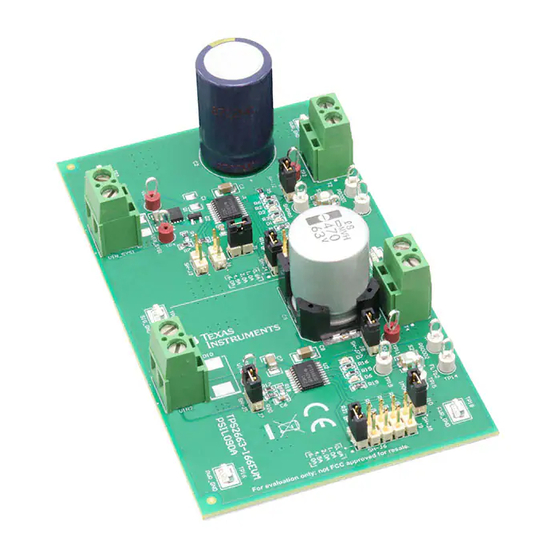
- Page 1 TPS2663-166EVM: Evaluation Module for TPS2663xPWP and TPS1663xPWP This user’s guide describes the evaluation module (EVM) for the Texas instruments TPS2663x and TPS1663x eFuse in PWP packages. The document provides EVM configuration information and test setup details for evaluating the TPS26633 and TPS16630 devices. The EVM schematic, board layout, and bill of materials (BOM) are also included.
- Page 2 • Electronic circuit breakers Description The TPS2663-166EVM enables evaluation of the TPS26633 and TPS16630 eFuses. This EVM has two channels: CH1 and CH2. CH1 is used with the TPS26633 device, whereas CH2 is used with the TPS16630 device. Table 1 provides the operating range and jumper settings for this EVM.
- Page 3 100nF TP16 TP17 TP19 SIG_GND TP18 3.0k 4.02k 9.09k SHDNb2 PWR_GND PWR_GND Figure 1. TPS2663-166EVM Schematic SLVUBQ5A – August 2019 – Revised October 2019 TPS2663-166EVM: Evaluation Module for TPS2663xPWP and TPS1663xPWP Submit Documentation Feedback Copyright © 2019, Texas Instruments Incorporated...
- Page 4 Signal ground for CH2 TP18 PWR_GND Output power ground for CH2 TP19 SHDNb2 Shutdown input signal for CH2 TPS2663-166EVM: Evaluation Module for TPS2663xPWP and TPS1663xPWP SLVUBQ5A – August 2019 – Revised October 2019 Submit Documentation Feedback Copyright © 2019, Texas Instruments Incorporated...
- Page 5 This jumper configures the device mode for overcurrent and overload conditions. MODE Configuration OPEN: Latch-Off (MODE = Open) for CH2 CLOSED: Auto-retry (MODE = GND) SLVUBQ5A – August 2019 – Revised October 2019 TPS2663-166EVM: Evaluation Module for TPS2663xPWP and TPS1663xPWP Submit Documentation Feedback Copyright © 2019, Texas Instruments Incorporated...
- Page 6 Turn ON the power supply and set the power supply output to 24 V and current limit to 10 A. • Turn OFF the power supply. TPS2663-166EVM: Evaluation Module for TPS2663xPWP and TPS1663xPWP SLVUBQ5A – August 2019 – Revised October 2019 Submit Documentation Feedback...
- Page 7 Test Equipment and Setup www.ti.com Table 5. Default Jumper Settings for TPS2663-166EVM Jumper For CH1 (TPS26633) Closed between Position Closed Closed Open Closed Open pin 1 and 2 For CH2 (TPS16630) Closed between Position Closed Closed Closed pin 1 and 2...
- Page 8 The device starts with inrush current of 0.5 A and the output voltage reaches V in 50 Figure 3 Figure 4 show examples of inrush current during start-up on the TPS2663-166EVM. Figure 3. TPS2663-166EVM Startup for CH1 (V = 24 V, Figure 4. TPS2663-166EVM Startup for CH2 (V...
- Page 9 Figure 5 Figure 6 show examples of the current limit at 4.5 A for CH1 and CH2, respectively, on the TPS2663-166EVM. Figure 5. TPS2663-166EVM Current Limit Operation for Figure 6. TPS2663-166EVM Current Limit Operation for CH1 (V = 24 V, I = 4.5 A, R...
- Page 10 Figure 7 Figure 8 show examples of output hot short on the TPS2663-166EVM. The device turns-off the internal MOSFET and disconnects the output from the input. Figure 7. TPS2663-166EVM Output Hot Short for CH1 (V Figure 8. TPS2663-166EVM Output Hot Short for CH2 (V...
- Page 11 , and I using an oscilloscope. Figure 9 shows an example of reverse input polarity protection on the TPS2663-166EVM. The device turns-off the internal MOSFET and disconnects the output from the input. Figure 9. TPS2663-166EVM Reverse Input Polarity for CH1 (V...
- Page 12 Observe the waveforms of V , FLT, and I using an oscilloscope. Figure 11 shows an example of overvoltage clamping on the TPS2663-166EVM for CH1. The device clamps the voltage to V voltage, turns off and retries. (OVC) Figure 11. TPS2663-166EVM Overvoltage Clamping for CH1 (V...
- Page 13 Figure 12. TPS2663-166EVM Top Overlay Figure 13. TPS2663-166EVM Bottom Overlay Figure 14. TPS2663-166EVM Top Layer Figure 15. TPS2663-166EVM Bottom Layer SLVUBQ5A – August 2019 – Revised October 2019 TPS2663-166EVM: Evaluation Module for TPS2663xPWP and TPS1663xPWP Submit Documentation Feedback Copyright © 2019, Texas Instruments Incorporated...
- Page 14 Bill of Materials www.ti.com Bill of Materials Table 6 lists the bill of materials for the TPS2663-166EVM. Table 6. TPS2663-166EVM BOM Designator Value Description Package Reference Part Number Manufacturer !PCB1 Printed circuit board PSIL090 1000 µF CAP, AL, 1000 µF, 50 V, ±20%, 0.034 Ω, AEC-Q200...
- Page 15 Evaluating TPS26631 and TPS26636 on TPS2663-166EVM www.ti.com Evaluating TPS26631 and TPS26636 on TPS2663-166EVM Uninstall the device U1 (TPS26633) and install the TPS26631 or TPS26636 device on the board. With the TPS26631 device, close jumper J6. With this configuration, the TPS26631 device selects a factory set...
- Page 16 Changes from Original (August 2019) to A Revision ..................... Page ......................... • Updated Section 6.1 title ........................• Updated Section 9 Revision History SLVUBQ5A – August 2019 – Revised October 2019 Submit Documentation Feedback Copyright © 2019, Texas Instruments Incorporated...
- Page 17 TI products. TI’s provision of these resources does not expand or otherwise alter TI’s applicable warranties or warranty disclaimers for TI products. Mailing Address: Texas Instruments, Post Office Box 655303, Dallas, Texas 75265 Copyright © 2019, Texas Instruments Incorporated...
Need help?
Do you have a question about the TPS2663-166EVM and is the answer not in the manual?
Questions and answers