Table of Contents
Advertisement
Quick Links
www.ti.com
User's Guide
TPS2661EVM: Evaluation Module for TPS2661x
Current-Loop Protector
This user's guide describes the evaluation module (EVM) for the Texas instruments TPS2661x current-loop
protector. The document provides EVM configuration information and test setup details for evaluating the
TPS26610 and TPS26612 devices. The EVM schematic, board layout, and bill of materials (BOM) are also
included.
The TPS26611, TPS26613 and TPS26614 devices can also be evaluated on this EVM by replacing
the TPS26610 (U1) device.
1
Introduction.............................................................................................................................................................................2
2 Description..............................................................................................................................................................................
3
Schematic................................................................................................................................................................................4
Configurations..........................................................................................................................................................5
Procedures....................................................................................................................................................7
6 EVAL Board Assembly Drawings and Layout Guidelines................................................................................................
(BoM)..........................................................................................................................................................24
8 Revision History...................................................................................................................................................................
Figure 3-1. TPS2661EVM eFuse Evaluation Board Schematic..................................................................................................
Figure 5-1. TPS2661EVM Setup With Test Equipment...............................................................................................................
Figure 5-4. TPS26610 Response During Recovery From Overload Fault..................................................................................
Figure 5-5. Output Short-Circuit Response of TPS26610 Device.............................................................................................
Figure 5-6. Output Short-Circuit Response of TPS26610 Device (Zoomed).............................................................................
Figure 5-10. Current-Limit Behavior of TPS26612....................................................................................................................
Figure 5-11. Current-Limit Behavior of TPS26612 Under Sustained Overload.........................................................................
Figure 5-16. IEC61000-4-5 (-1 kV, 42 Ω) Signal Line Surge Immunity With TVS3301 at Output of CH2.................................
Figure 6-1. TPS2661EVM Board Assembly..............................................................................................................................
Figure 6-2. TPS2661EVM Board Top Layer..............................................................................................................................
Table 2-1. TPS2661EVM eFuse Evaluation Board Options and Setting.....................................................................................
Table 4-1. Input and Output Connector Functionality..................................................................................................................
Table 4-2. Test Points Description...............................................................................................................................................
SLVUBX8B - OCTOBER 2020 - REVISED DECEMBER 2021
Submit Document Feedback
ABSTRACT
Note
Table of Contents
List of Figures
> 2 × I
With MODE = 180 kΩ .........................................................
OUT
OL
Device..............................................................................12
Device...........................................................................13
Device.............................................................................14
...............................................................................................17
Layer.........................................................................................................................23
List of Tables
Copyright © 2021 Texas Instruments Incorporated
(Zoomed).........................................9
CH1....................................18
CH1....................................19
CH2.................................20
TPS2661EVM: Evaluation Module for TPS2661x
Current-Loop Protector
Table of Contents
3
22
26
4
7
8
9
10
11
15
16
21
22
22
3
5
5
1
Advertisement
Table of Contents

Related Manuals for Texas Instruments TPS2661EVM


Summary of Contents for Texas Instruments TPS2661EVM
-
Page 1: Table Of Contents
Current-Loop Protector ABSTRACT This user’s guide describes the evaluation module (EVM) for the Texas instruments TPS2661x current-loop protector. The document provides EVM configuration information and test setup details for evaluating the TPS26610 and TPS26612 devices. The EVM schematic, board layout, and bill of materials (BOM) are also included. -
Page 2: Introduction
All trademarks are the property of their respective owners. 1 Introduction The TPS2661EVM allows reference circuit evaluation of the TPS26610 and TPS26612 current-loop protector from TI. The TPS2661x device is a 50-V, universal (±20 mA, 0 to 20 mA, 4–20 mA) current-loop protector with integrated fixed bipolar 30-mA current limit and output overvoltage protection. -
Page 3: Description
Description 2 Description The TPS2661EVM evaluation board enables evaluation of TPS26610 and TPS26612 current loop protectors. The input signal is applied between connectors J1 and J13 while J3 and J9 provides the output connection to the load; see the schematic in... -
Page 4: Schematic
AGND_2 AGND_2 AGND_2 AGND_2 12.1k 8.06k 4.02k AGND_2 AGND_2 Figure 3-1. TPS2661EVM eFuse Evaluation Board Schematic TPS2661EVM: Evaluation Module for TPS2661x Current-Loop Protector SLVUBX8B – OCTOBER 2020 – REVISED DECEMBER 2021 Submit Document Feedback Copyright © 2021 Texas Instruments Incorporated... -
Page 5: General Configurations
General Configurations 4 General Configurations 4.1 Physical Access Table 4-1 lists the TPS2661EVM evaluation board input and output connector functionality. Table 4-2 Table describe the test point availability and the jumper functionality. Table 4-1. Input and Output Connector Functionality... - Page 6 A DPO2024 or equivalent, three 10 × voltage probes, and a DC current probe. 4.2.4 Loads One decade resistance box or equivalent which can tolerate 50 V and capable of the output short. TPS2661EVM: Evaluation Module for TPS2661x SLVUBX8B – OCTOBER 2020 – REVISED DECEMBER 2021 Current-Loop Protector Submit Document Feedback Copyright ©...
-
Page 7: Test Setup And Procedures
In this user's guide, the test procedure is described for the TPS26610 and TPS26612 devices. Make sure the evaluation board has default jumper settings as shown in Table 5-1. Table 5-1. Default Jumper Setting for TPS2661EVM eFuse Evaluation Board 1–2 Open Open... -
Page 8: Figure 5-2. Current Limit Behavior Of Tps26610 For I
6. Step-down the voltage at I_IN_1 to 1.6 V to remove the overload fault Figure 5-2 Figure 5-3 show current limit behavior captured on the TPS2661EVM eFuse Evaluation Board. Figure 5-4 shows device response during recovery from overload fault. Figure 5-2. Current Limit Behavior of TPS26610 for I >... -
Page 9: Figure 5-3. Current Limit Behavior Of Tps26610 For Iout Ol
> 2 × I With MODE = 180 kΩ (Zoomed) Figure 5-4. TPS26610 Response During Recovery From Overload Fault SLVUBX8B – OCTOBER 2020 – REVISED DECEMBER 2021 TPS2661EVM: Evaluation Module for TPS2661x Submit Document Feedback Current-Loop Protector Copyright © 2021 Texas Instruments Incorporated... -
Page 10: Figure 5-5. Output Short-Circuit Response Of Tps26610 Device
Figure 5-6 show test waveforms of output hot-short on the TPS2661 eFuse evaluation board. Figure 5-5. Output Short-Circuit Response of TPS26610 Device TPS2661EVM: Evaluation Module for TPS2661x SLVUBX8B – OCTOBER 2020 – REVISED DECEMBER 2021 Current-Loop Protector Submit Document Feedback... -
Page 11: Figure 5-6. Output Short-Circuit Response Of Tps26610 Device (Zoomed)
Test Setup and Procedures Figure 5-6. Output Short-Circuit Response of TPS26610 Device (Zoomed) SLVUBX8B – OCTOBER 2020 – REVISED DECEMBER 2021 TPS2661EVM: Evaluation Module for TPS2661x Submit Document Feedback Current-Loop Protector Copyright © 2021 Texas Instruments Incorporated... -
Page 12: Figure 5-7. Input Undervoltage Protection Response Of Tps26610
4. Apply a voltage of 0 V at I_IN_1 and gradually decrease the voltage to –15.4 V to trigger the input undervoltage fault 5. Observe the waveforms using an oscilloscope Figure 5-7 shows input undervoltage protection response of TPS26610 on TPS2661EVM eFuse Evaluation Board. Figure 5-7. Input Undervoltage Protection Response of TPS26610 Device TPS2661EVM: Evaluation Module for TPS2661x SLVUBX8B –... -
Page 13: Figure 5-8. Output Undervoltage Protection Response Of Tps26610
4. Observe the waveforms using an oscilloscope Figure 5-8 shows output undervoltage protection response of TPS26610 on TPS2661EVM eFuse Evaluation Board. Figure 5-8. Output Undervoltage Protection Response of TPS26610 Device SLVUBX8B – OCTOBER 2020 – REVISED DECEMBER 2021... -
Page 14: Figure 5-9. Output Overvoltage Protection Response Of Tps26610
3. Apply a voltage of 0 V at I_OUT_1 and gradually increase the voltage to 15.3 V to trigger the output overvoltage fault 4. Observe the waveforms using an oscilloscope Figure 5-9 shows output overvoltage protection response of TPS26610 on TPS2661EVM eFuse evaluation board. Figure 5-9. Output Overvoltage Protection Response of TPS26610 Device TPS2661EVM: Evaluation Module for TPS2661x SLVUBX8B –... -
Page 15: Figure 5-10. Current-Limit Behavior Of Tps26612
4. Now apply load of 5 Ω between I_OUT_2 and AGND_2 to trigger overload fault 5. Observe the waveforms using an oscilloscope Figure 5-10 Figure 5-11 show current limit behavior of TPS26612 captured on the TPS2661EVM eFuse evaluation board. Figure 5-10. Current-Limit Behavior of TPS26612 SLVUBX8B – OCTOBER 2020 – REVISED DECEMBER 2021... -
Page 16: Figure 5-11. Current-Limit Behavior Of Tps26612 Under Sustained Overload
7. The device limits the current to 32 mA for approximately 100 ms and then auto retries for every 800 ms Figure 5-12 shows current limit behavior captured on the TPS2661EVM with TPS26613 in U1 position. TPS2661EVM: Evaluation Module for TPS2661x SLVUBX8B –... - Page 17 Test Setup and Procedures VOUT SGOODb I_IN Figure 5-12. Current Limit Behavior of TPS26613 for V < –V SLVUBX8B – OCTOBER 2020 – REVISED DECEMBER 2021 TPS2661EVM: Evaluation Module for TPS2661x Submit Document Feedback Current-Loop Protector Copyright © 2021 Texas Instruments Incorporated...
-
Page 18: Figure 5-13. Iec61000-4-5 (+1 Kv, 42 Ω) Signal Line Surge Immunity With Tvs3301 At Input Of Ch1
6. Observe the waveforms using an oscilloscope Figure 5-13 Figure 5-14 show surge performance for current inputs with TPS26610 on the TPS2661EVM eFuse evaluation board. Figure 5-13. IEC61000-4-5 (+1 kV, 42 Ω) Signal Line Surge Immunity With TVS3301 at Input of CH1 TPS2661EVM: Evaluation Module for TPS2661x SLVUBX8B –... -
Page 19: Figure 5-14. Iec61000-4-5 (-1 Kv, 42 Ω) Signal Line Surge Immunity With Tvs3301 At Input Of Ch1
Test Setup and Procedures Figure 5-14. IEC61000-4-5 (–1 kV, 42 Ω) Signal Line Surge Immunity With TVS3301 at Input of CH1 SLVUBX8B – OCTOBER 2020 – REVISED DECEMBER 2021 TPS2661EVM: Evaluation Module for TPS2661x Submit Document Feedback Current-Loop Protector Copyright © 2021 Texas Instruments Incorporated... -
Page 20: Figure 5-15. Iec61000-4-5 (+1 Kv, 42 Ω) Signal Line Surge Immunity With Tvs3301 At Output Of Ch2
6. Observe the waveforms using an oscilloscope Figure 5-15 Figure 5-16 show surge performance for current inputs with TPS26610 on the TPS2661EVM eFuse evaluation board. Figure 5-15. IEC61000-4-5 (+1 kV, 42 Ω) Signal Line Surge Immunity With TVS3301 at Output of CH2 TPS2661EVM: Evaluation Module for TPS2661x SLVUBX8B –... -
Page 21: Figure 5-16. Iec61000-4-5 (-1 Kv, 42 Ω) Signal Line Surge Immunity With Tvs3301 At Output Of Ch2
Test Setup and Procedures Figure 5-16. IEC61000-4-5 (–1 kV, 42 Ω) Signal Line Surge Immunity With TVS3301 at Output of CH2 SLVUBX8B – OCTOBER 2020 – REVISED DECEMBER 2021 TPS2661EVM: Evaluation Module for TPS2661x Submit Document Feedback Current-Loop Protector Copyright © 2021 Texas Instruments Incorporated... -
Page 22: Eval Board Assembly Drawings And Layout Guidelines
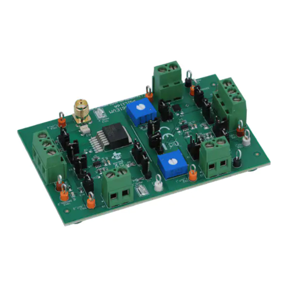
6-2, Figure 6-3 show PCB layout images. Figure 6-1. TPS2661EVM Board Assembly Figure 6-2. TPS2661EVM Board Top Layer TPS2661EVM: Evaluation Module for TPS2661x SLVUBX8B – OCTOBER 2020 – REVISED DECEMBER 2021 Current-Loop Protector Submit Document Feedback Copyright © 2021 Texas Instruments Incorporated... -
Page 23: Figure 6-3. Tps2661Evm Board Bottom
EVAL Board Assembly Drawings and Layout Guidelines Figure 6-3. TPS2661EVM Board Bottom Layer SLVUBX8B – OCTOBER 2020 – REVISED DECEMBER 2021 TPS2661EVM: Evaluation Module for TPS2661x Submit Document Feedback Current-Loop Protector Copyright © 2021 Texas Instruments Incorporated... -
Page 24: Bill Of Materials (Bom)
RT0603BRD0747KL Yageo America 6.73 k RES, 6.73 k, 0.1%, 0.1 W, 0603 0603 RT0603BRD076K73L Yageo America TPS2661EVM: Evaluation Module for TPS2661x Current-Loop Protector SLVUBX8B – OCTOBER 2020 – REVISED DECEMBER 2021 Submit Document Feedback Copyright © 2021 Texas Instruments Incorporated... - Page 25 Bill Of Materials (BoM) Table 7-1. TPS2661EVM Bill of Materials (continued) Alternate Part Alternate Designator Value Description Package Reference Part Number Manufacturer Number Manufacturer 6.04 RES, 6.04 M, 1%, 0.1 W, AEC-Q200 Grade 0, 0603 0603 CRCW06036M04FKEA Vishay-Dale 1.00 RES, 1.00 M, 0.5%, 0.1 W, AEC-Q200 Grade 0, 0603...
-
Page 26: Revision History
• Added surge test waveforms and Surge Protection Test (Analog Output, CH2) section........20 • Updated TPS2661EVM board assembly and layer images in Section 6.1............22 • Updated bill of materials........................... TPS2661EVM: Evaluation Module for TPS2661x SLVUBX8B – OCTOBER 2020 – REVISED DECEMBER 2021... - Page 27 STANDARD TERMS FOR EVALUATION MODULES Delivery: TI delivers TI evaluation boards, kits, or modules, including any accompanying demonstration software, components, and/or documentation which may be provided together or separately (collectively, an “EVM” or “EVMs”) to the User (“User”) in accordance with the terms set forth herein.
- Page 28 www.ti.com Regulatory Notices: 3.1 United States 3.1.1 Notice applicable to EVMs not FCC-Approved: FCC NOTICE: This kit is designed to allow product developers to evaluate electronic components, circuitry, or software associated with the kit to determine whether to incorporate such items in a finished product and software developers to write software applications for use with the end product.
- Page 29 www.ti.com Concernant les EVMs avec antennes détachables Conformément à la réglementation d'Industrie Canada, le présent émetteur radio peut fonctionner avec une antenne d'un type et d'un gain maximal (ou inférieur) approuvé pour l'émetteur par Industrie Canada. Dans le but de réduire les risques de brouillage radioélectrique à...
- Page 30 www.ti.com EVM Use Restrictions and Warnings: 4.1 EVMS ARE NOT FOR USE IN FUNCTIONAL SAFETY AND/OR SAFETY CRITICAL EVALUATIONS, INCLUDING BUT NOT LIMITED TO EVALUATIONS OF LIFE SUPPORT APPLICATIONS. 4.2 User must read and apply the user guide and other available documentation provided by TI regarding the EVM prior to handling or using the EVM, including without limitation any warning or restriction notices.
- Page 31 Notwithstanding the foregoing, any judgment may be enforced in any United States or foreign court, and TI may seek injunctive relief in any United States or foreign court. Mailing Address: Texas Instruments, Post Office Box 655303, Dallas, Texas 75265 Copyright © 2019, Texas Instruments Incorporated...
- Page 32 TI products. TI’s provision of these resources does not expand or otherwise alter TI’s applicable warranties or warranty disclaimers for TI products. TI objects to and rejects any additional or different terms you may have proposed. IMPORTANT NOTICE Mailing Address: Texas Instruments, Post Office Box 655303, Dallas, Texas 75265 Copyright © 2021, Texas Instruments Incorporated...
Need help?
Do you have a question about the TPS2661EVM and is the answer not in the manual?
Questions and answers