Table of Contents
Advertisement
Quick Links
Advertisement
Table of Contents

Related Manuals for Epson S2R72A21


Summary of Contents for Epson S2R72A21
- Page 1 S2R72A21 Application Note Rev.1.00...
- Page 2 Seiko Epson. Seiko Epson reserves the right to make changes to this material without notice. Seiko Epson does not assume any liability of any kind arising out of any inaccuracies contained in this material or due to its application or use in any product or circuit and, further, there is no representation that this material is applicable to products requiring high level reliability, such as, medical products.
-
Page 3: Table Of Contents
Role Switch control ......................19 5.3.4 Method to detect disconnection of Portable Device ............19 6. USB Compliance test ....................21 S2R72A21 function aimed at USB compliance test ............21 General Test method ......................21 6.2.1 High-speed Signal Quality ....................21 6.2.2... - Page 4 7. PCB design guide ....................27 Power supply and reset ....................... 27 DP/DM signal line ......................... 27 7.2.1 Circuit board wiring ......................27 7.2.2 Additional component ...................... 27 Oscillator circuit ........................29 Others precautions ......................29 Revision History......................31 Seiko Epson Corporation S2R72A21 Application Note (Rev.1.00)
-
Page 5: Description
This document explains the USB connection description, system implementation, compliance test for products which equip S2R72A21 as well as the remark point during PCB designing using this Re-Synchronization IC. Please refer to the S2R72A21 data sheet for Hardware related information. -
Page 6: Terms & Abbreviations
Definition Operation when the cable is inserted or the moment when it is Attach inserted ADJ pin The pin of S2R72A21 which setup the HS transmit current Battery Charge BC Regulator Regulator which correspond to BC specification Bus Reset Bus reset which invoke HS detection handshake... -
Page 7: Operation
The objective paths are switched automatically by the internal Bus Monitor. Basic system structure As the basic system structure, here shows an example where S2R72A21 is mounted on the Car Navigation or Display Audio’s board (Host SoC board). S2R72A21 intervenes between the Host SoC’s USB port and the USB type-A receptacle, and connects the Host SoC (as Host) and Portable device such as smart phones (as Device). - Page 8 Please connect the Host SoC’s USB OTG port in case Role Switch is executed. It is possible to connect the BC Regulator for VBUS supply between the Host SoC’s USB OTG port and the S2R72A21’s INT port. BC Regulator can select the VBUS supply capability by negotiation with BC capable Portable Device.
-
Page 9: Basic Operation
Basic operation The basic operation of the S2R72A21 under the above basic system structure is explained based on an example of the USB2.0+BC operation waveform. 3.3.1 Operation waveform Figure 3.3.1.1 shows an example of the S2R72A21 operation waveform on the basic system structure of Figure 3.2.1. -
Page 10: Each Operation
After detecting “Chirp K-J-K-J-K-J”, the Portable Device would also enable its HS termination. Due to this, Chirp K-J’s amplitude would change from 800mV to 400mV. S2R72A21 would detect this line of Chirp operation with Bus Monitor, and wait until this Chirp sequence is finished. - Page 11 3.3.2.6 HS operation (1) After the Chirp K-J delivery to the INT port from the Host SoC is finished, the S2R72A21 would judge that the Chirp is finished by SE0 detection and it would transit to HS state. During this period, the USB signal path would be switched from Bus Switch to HS Synchronizer. Please wait over 5us until the first SOF transmit start from the Chirp delivery from the Host SoC is finished.
- Page 12 3.3.2.11 Operation end The Host SoC can notify the Detach detection to the S2R72A21 by ENABLE=0 once the Host SoC has detected the Detach of the Portable Device. The S2R72A21 would transit to DISCONNECT state when ENABLE=0. Here the connection of the INT port and the EXT port is maintained. Both the INT port and the EXT port would be VSS level due to the pull down resistor of the Host SoC.
-
Page 13: Hs Transmission Current Control
HS packets transmitted from the Host are re-synchronized by S2R72A21, and reach the Device through the USB Cable. P1 is the signal measuring point at the S2R72A21 pin, and P2 is the signal measuring point at the Device. The HS signal transmitted from the S2R72A21 is attenuated by the USB cable, etc., thus the signal amplitude at P1 is greater than that at P2 as shown in the figure. -
Page 14: Connection Example
Connection example Please refer to the following in regard to the 3 system connection examples using S2R72A21. Please refer to Chapter 5 for detail operation of each connection examples. In addition, “EP” in the drawing stands for Exposed die pad. -
Page 15: Connection Ex. Host Soc (On The Separate Board)/Int Port, Portable Device/Ext Port
Host SoC board Host SoC Portable HVDD Device STAT1 Regulator STAT0 S2R72A21 VBUS VBUS EXT_DP INT_DP EXT_DM INT_DM Figure 4.3.1 Connection ex. Host SoC (on the separate board)/EXT port, Portable Device/INT port Seiko Epson Corporation S2R72A21 Application Note (Rev.1.00) -
Page 16: Operation Within Each Connection Example
3ms of SE0 is detected and the Bus Switch connection between INT-EXT would be valid. In other words, within the above Role switch operation sequence, S2R72A21 would detect over 3ms of SE0, automatically validate the Bus Switch in between INT-EXT for FS communication, and transit to HS communication connection condition after Role Switch. -
Page 17: Connection Ex. Host Soc (On The Same Board)/Int Port, Portable Device/Ext Port
ADJ settings S2R72A21 is mounted on the same board as the Host SoC. Each of the ADJ4 pin (SDA pin) and ADJ3 (SCL pin) are connected with the SoC’s I2C master. In this case, the HS transmit current control can all be possible to set entire 4bit for both the INT and the EXT port by setting SEL_I2C=1 setting via I2C register. - Page 18 Since the periodic SOF sent from the Portable Device (as Host) is lost, the SE0 would be detected by EXT port’s Bus state. When the S2R72A21 detects the SE0 condition for 3ms by the Bus state, the HS Synchronizer’s operation would stop and the FS_LS state transition is done where the Bus Switch path between INT-EXT gets “ON”.
-
Page 19: Connection Ex. Host Soc (On The Separate Board)/Int Port, Portable Device/Ext Port
ADJ settings The S2R72A21 would be connected to the Host SoC via USB cables only, so the HS transmit current control function via the I2C register cannot be used. In this case please set SEL_I2C=0 and follow, section 4.2 control pin of the S2R72A21 data sheet and set up the HS transmit current control function by ADJ2-0. - Page 20 The disconnection detection notification cannot be done via the ENABLE pin since this connection example would be done via USB cable only (between Host SoC and S2R72A21). In this case please reset the S2R72A21 as indicated above at 3Steps (Stop the VBUS supply and then resuming it). Please refer to the AC characteristics on the Data sheet for the timings (VBUS supply stop to resume).
-
Page 21: Connection Ex. Host Soc (On The Separate Board)/Ext Port, Portable Device/Int Port
ADJ settings The S2R72A21 would be connected to the Host SoC via USB cables only, so the HS transmit current control function via the I2C register cannot be used. In this case please set SEL_I2C=0 and follow, section 4.2 control pin of the S2R72A21 data sheet and set up the HS transmit current control function by ADJ2-0. - Page 22 The disconnection detection notification cannot be done via the ENABLE pin since this connection example would be done via USB cable only (between Host SoC and S2R72A21). In this case please reset the S2R72A21 as indicated above at 3Steps (Stop the VBUS supply and then resuming it). Please refer to the AC characteristics on the Data sheet for the timings (VBUS supply stop to resume).
-
Page 23: Usb Compliance Test
Also it has a feature to transmit the High-speed J/K to the other port, when HS Test J/ Test K are detected from one port. Please set “0” to either ENABLE pin or XRESET pin of S2R72A21 to recover from this condition. -
Page 24: Test J / K
Test J / K Here is the explanation of the S2R72A21’s output methods of High-speed J/K. It is similar to the method explained on section 6.2.1. Please make the Host output the High-Speed J/K via Test J/K mode instead of Test Packet. -
Page 25: Test Procedure
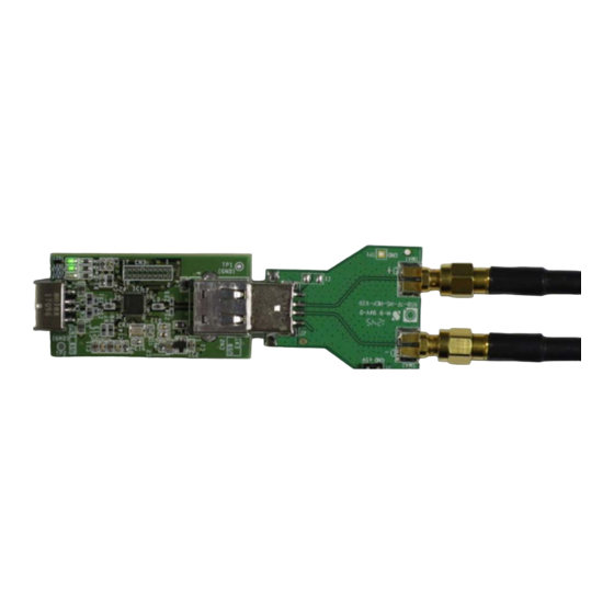
15443A Matched Cable Pair 6.3.2 Test procedure Connect the Host PC and the S2R72A21 Evaluation board (INT port side). Figure 6.3.2.1 Procedure-1 connection Connect the HS USB memory to the S2R72A21evaluation board’s EXT port, and check whether there is HS connection between the Host PC and the HS memory. - Page 26 Push EXECUTE after inputting the Port # connected to the S2R72A21evaluation board. With this operation, the Test Packet would be output from the Host PC, and then output from the EXT port via S2R72A21’s HS Synchronizer. Figure 6.3.2.5 Procedure-5 (HS Electrical Test Tool picture)
-
Page 27: Cautions For Each Test
As stated on section 6.3 of the data sheet, a packet delay would occur during HS packet re-synchronization. When the system with S2R72A21 is tested as a Host, the total period of the Host Controller’s response and the round-trip delay of S2R72A21 would be observed as the total system’s period. Due to this, there would be a possibility exceeding the max response period of 192 bit times (stated on the EL_22). -
Page 28: Contact Window Regarding Compliance Test
Epson has explained the product characteristics of the USB2.0 Re-Synchronization IC to Allion and Granite River Labs Japan Ltd. (GRL). Please contact the following Allion or GRL window for compliance testing in relates to product using S2R72A21. If the contact person is unknown, please ask Epson’s local sales window. -
Page 29: Pcb Design Guide
The following is the explanation in regard to power supply related topic towards the S2R72A21. • Power on / Power down sequence The power supplied to S2R72A21 is only HVDD (3.3V). There is no Power on / Power down sequence since there is a built in regulator. 1.8V can be supplied internally. •... - Page 30 • Chip varistor Use on the DP/DM signal line can be effective in protecting the S2R72A21’s DP/DM pins from static electricity and surges. Typical components used for USB High-speed are listed below. Note that components should preferably be installed with shortest possible branches from the signal line to ensure signal quality. The chip varistor mounting position is generally considered more effective in the vicinity of the connectors, but this should be determined after consulting with the respective manufacturers.
-
Page 31: Oscillator Circuit
Bypass capacitors as close as possible to each HVDD pin. The capacitance amount on Epson’s evaluation board is as following, but it would vary depending on the regulator’s characteristics. Epson also recommends this to be assembled towards each power supply pin to ensure a stable IC’s operation. - Page 32 Each HVDD pin: 0.1uF Power supply source: 10uF • VSS pins The VSS pins must be connected to a non-separated GND plane via low impedance. Seiko Epson Corporation S2R72A21 Application Note (Rev.1.00)
-
Page 33: Revision History
Revision History Attachment-1 Rev. No. Date Section Category Contents Rev. 1.00 9/12/2020 New issue Seiko Epson Corporation S2R72A21 Application Note (Rev.1.00) - Page 34 FAX: +86-10-3299-0560 Riesstrasse 15, 80992 Munich, Germany Phone: +49-89-14005-0 FAX: +49-89-14005-110 Epson Taiwan Technology & Trading Ltd. 15F, No.100, Songren Rd, Sinyi Dist, Taipei City 110. Taiwan Phone: +886-2-8786-6688 Epson Singapore Pte., Ltd. 438B Alexandra Road, Block B Alexandra TechnoPark, #04-01/04, Singapore 119968...
Need help?
Do you have a question about the S2R72A21 and is the answer not in the manual?
Questions and answers