Table of Contents
Advertisement
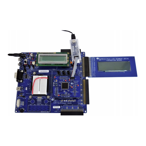
Quick Links
Advertisement
Table of Contents

Related Manuals for Cypress PSoC CY8CKIT-029A


Summary of Contents for Cypress PSoC CY8CKIT-029A
- Page 1 ® CY8CKIT-029 PSoC LCD Segment Drive Expansion Board Kit Guide Doc. # 001-55415 Rev. *K Cypress Semiconductor 198 Champion Court San Jose, CA 95134-1709 Phone (USA): 800.858.1810 Phone (Intnl): 408.943.2600 http://www.cypress.com Arrow.com. Downloaded from...
- Page 2 Cypress Source Code and derivative works for the sole purpose of creating custom soft- ware and or firmware in support of licensee product to be used only in conjunction with a Cypress integrated circuit as speci- fied in the applicable agreement.
-
Page 3: Table Of Contents
Contents Safety Information 1. Introduction Kit Contents .........................7 PSoC Creator ......................7 Getting Started......................8 Additional Learning Resources..................8 1.4.1 Beginner Resources..................8 1.4.2 Engineers Looking for More ................8 1.4.3 Learning from Peers..................8 1.4.4 More Code Examples..................8 Document Conventions .....................10 2. Installation CD Installation ......................11 Install Hardware......................12 Install Software ......................12 Verify Kit version ......................12... - Page 4 Contents 5. Code Examples Code Example 1: LCD_Seg_Example1_Battery_Meter..........29 5.1.1 Project Description..................29 5.1.2 Running the Code Example ................29 5.1.3 Hardware Connections .................. 29 5.1.4 Verifying Output ..................... 30 5.1.5 PSoC Creator Project Details ................ 30 5.1.5.1 LCD_Seg ..................30 5.1.5.2 ADC_DelSig ..................
-
Page 5: Safety Information
Safety Information Regulatory Compliance The CY8CKIT-029 is intended for use as a development platform for hardware or software in a laboratory environment. The board is an open system design, which does not include a shielded enclosure. This may cause interference to other electrical or electronic devices in close proximity. In a domestic environment, this product may cause radio interference. - Page 6 General Safety Instructions Electrostatic Discharge (ESD) Protection ESD can damage boards and associated components. Cypress recommends that you perform procedures only at an ESD workstation. If one is not available, use appropriate ESD protection by wearing an antistatic wrist strap attached to chassis ground (any unpainted metal surface) on your board when handling parts.
-
Page 7: Introduction
Quick Start Guide ■ Kit CD ■ Inspect the contents of the kit; if you do not find any part, contact your nearest Cypress sales office for help. PSoC Creator Cypress's PSoC Creator software is a state-of-the-art, easy-to-use software development Integrated Development Environment (IDE). -
Page 8: Getting Started
® AN52927 - PSoC 3 and PSoC 5LP - Segment LCD Direct Drive. Cypress continually strives to provide the best support. Click here to view a growing list of application notes for PSoC 3, PSoC 4 and PSoC 5LP. 1.4.3... - Page 9 Introduction Figure 1-1. Find Example Project The Find Example Project section has various filters that help you locate the most relevant project. PSoC Creator provides several starter designs. These designs highlight features that are unique to PSoC devices. They allow you to create a design with various components, instead of creating an empty design;...
-
Page 10: Document Conventions
Introduction The example projects and starter designs are designed for the CY8CKIT-001 PSoC Development Kit. However, these projects can be converted for use with the CY8CKIT-030 PSoC 3 Development Kit or CY8CKIT-050 PSoC 5LP Development Kit by following the procedure in the knowledge base article Migrating Project from CY8CKIT-001 to CY8CKIT-030 or CY8CKIT-050 Document Conventions... -
Page 11: Installation
Installation CD Installation Follow these steps to install the CY8CKIT-029 PSoC LCD Segment Drive EBK software: 1. Insert the kit CD into the CD drive of your computer. The CD is designed to auto-run and the PSoC LCD Segment Drive EBK menu appears. Figure 2-1. -
Page 12: Install Hardware
To know the kit revision, look for the white sticker on the back of the kit box. If the revision reads CY8CKIT-029 Rev **, then congratulations, you own the latest version. You can purchase the latest version of the kit at http://www.cypress.com/go/CY8CKIT-029. CY8CKIT-029 PSoC® LCD Segment Drive Expansion Board Kit Guide, Doc. # 001-55415 Rev. *K Arrow.com. -
Page 13: Kit Operation
Kit Operation Introduction The CY8CKIT-029 PSoC LCD Segment Drive EBK code examples are designed using a display with many segments (8 common lines by 16 segment lines giving 128 segments). Code Example 1: LCD_Seg_Example1_Battery_Meter ■ This example demonstrates the battery charge indicator along with the 14-segment display of the LCD glass by implementing a battery meter. - Page 14 Kit Operation Figure 3-1. PSoC 3 Processor Module, Power, and MiniProg3 Connection with CY8CKIT-001 DVK Note See the CY8CKIT-001_PSoC_Development_Kit_Guide in www.cypress.com/go/cy8ckit-001 for details on connecting and programming PSoC devices. 4. Click on the relevant code example i.e., LCD_Seg_Example1_Battery_Meter_009A for PSoC 3 module and LCD_Seg_Example1_Battery_Meter_010LP for PSoC 5LP module, located in Examples and Kits on the Start Page of PSoC Creator.
- Page 15 Kit Operation 5. Create a folder in the desired location and click OK. The project opens in PSoC Creator and is saved in that folder. 6. Build the project by selecting the Build option. Figure 3-3. Build Project 7. Click the Program icon. Figure 3-4.
-
Page 16: Programming A Psoc 3/Psoc 5Lp Development Kit
Kit Operation 3.2.2 Programming a PSoC 3/PSoC 5LP Development Kit This section provides details on programming the PSoC 3/ PSoC 5LP Development Kit. The default programming interface for the board is a USB based on-board programming interface. To program the device, follow the following steps: 1. - Page 17 Kit Operation 3. Create a folder in the desired location and click OK. The project opens in PSoC Creator and is saved in that folder. 4. Build the project by selecting the Build option. Figure 3-9. Build Project 5. Click the Program icon. Figure 3-10.
-
Page 18: Hardware Connection
Kit Operation Hardware Connection 3.3.1 Hardware Connection for CY8CKIT-001 DVK Note: The Hardware Connection on page 18 Verify the Output on page 20 describe the Example1_Battery_Metercode example. Please refer Code Example LCD_Seg_Example2_StopWatch on page 37 for details on Example2_StopWatch code example. Configure the DVK SW3 to 3.3 V. -
Page 19: Hardware Connections For Psoc 3/Psoc 5Lp Development Kit
Power the VR by setting jumper J11 to the ‘ON’ position. Figure 3-14. Jumper J11 in ON Position on CY8CKIT-001 DVK Note: The remaining jumper settings on the DVK have the default state. See the CY8CKIT-001_PSoC_Development_Kit_Guide in www.cypress.com/go/cy8ckit-001 for default setting of the jumpers. 3.3.2 Hardware Connections for PSoC 3/PSoC 5LP Development Kit 1. -
Page 20: Verify The Output
Kit Operation Verify the Output Vary the VR (potentiometer) and note the change in status displayed on the LCD. Figure 3-15. Verifying Output of Battery Meter Project Note The best viewing angle is from 6 o’clock, according to the LCD glass characteristics. CY8CKIT-029 PSoC®... -
Page 21: Hardware
Hardware System Block Diagram The PSoC LCD Segment Drive EBK consists of only three blocks. LCD glass (Golden View Display LCD, GV13956A-TPP) ■ I2C EEPROM (ST, M24C02-W) ■ 40-pin (20x2) connector (Sullins Connector Solutions, S2111E-20-ND) ■ Figure 4-1. System Block Diagram This board includes a custom LCD glass with maximum 128 segments. -
Page 22: Functional Description
Hardware Functional Description 4.2.1 LCD Glass Details Figure 4-2 shows the image of the LCD glass and Table 4-1 lists the segment details. The LCD glass provides visual feedback. Figure 4-2. LCD Glass Table 4-1. LCD Glass Segment Details Label Description Battery charge indicator bars Wireless symbol... -
Page 23: Glass Specification
Hardware The following figure shows the segment lettering information for all LCD segments. Figure 4-3. Segment Lettering Information Note Pixel mapping table is also available on the back of the CY8CKIT-029 PSoC LCD Segment Drive EBK. 4.2.1.2 Glass Specification Display type: TN ■... - Page 24 Hardware Table 4-2. Port Pin Connections Port A Port A’ Port B PSoC EBK P3_7 P6_7 P1_7 SEG15 P3_6 P6_6 P1_6 SEG14 P3_5 P6_5 P1_5 SEG13 P3_4 P6_4 P1_4 SEG12 P3_3 P6_3 P1_3 SEG11 P3_2 P6_2 P1_2 SEG10 P3_1 P6_1 P1_1 SEG9 P3_0...
- Page 25 Hardware Jumper Settings of CY8CKIT-001 DVK to Use Port A' and Port B: Both port A' and port B uses the port 2 pins for segment lines. Switch the jumper J12 to the ‘OFF’ position; this switches off power to the character LCD, which is connected to port 2 of the CY8CKIT- 001 DVK.
-
Page 26: Port Options With Cy8Ckit-030/Cy8Ckit-050Lp Dvk
Hardware Port Options with CY8CKIT-030/CY8CKIT-050LP DVK The code examples provided with the kit uses Port D of CY8CKIT-030 and CY8CKIT-050LP. The code examples can be converted to use Port E of the kit by changing the pin connection in the DWR file of the project. - Page 27 Hardware Table 4-3. Pin Assignment Table (continued) Port D Port E PSoC LCD EBK Port D uses Port 2 for segment lines. So, the Character LCD should be removed from LCD port while using Port D. PSoC provides serial wire debugging (SWD) with SWD on GPIO pins option. The port pins used for SWD are P1_0 (SWDIO) and P1_1 (SWDCK).
-
Page 28: Power Supply
Hardware Power Supply The kit is powered from the DVK through the 40-pin (2×20) connector. CY8CKIT-029 PSoC® LCD Segment Drive Expansion Board Kit Guide, Doc. # 001-55415 Rev. *K Arrow.com. Arrow.com. Arrow.com. Arrow.com. Arrow.com. Arrow.com. Arrow.com. Arrow.com. Arrow.com. Arrow.com. Arrow.com. Arrow.com. -
Page 29: Code Examples
Code Examples Code Example 1: LCD_Seg_Example1_Battery_Meter This code example demonstrates the battery charge indicator along with the 14-segment display of the LCD glass by implementing a battery meter. The battery meter is used to graphically display the battery charge level; the 14-segment display is used to relay messages related to the battery charge (full, medium, and low). -
Page 30: Verifying Output
Code Examples Hardware Connections for PSoC 3/PSoC 5LP Development Kit on page 19 for details on hard- ware connections on CY8CKIT-030/CY8CKIT-050LP. 5.1.4 Verifying Output Vary the VR (potentiometer) and note the status changes displayed on the LCD. Figure 5-2. Verification of Battery Meter Project 5.1.5 PSoC Creator Project Details PSoC Creator offers a flexible software tool to create and configure the programmable peripherals. - Page 31 Code Examples between 0 and 127 with 127 corresponding to the maximum contrast level. The frame rate is selected to be the maximum rate before the characters in the display begin to reduce in contrast. The segment LCD component in this code example is used to control the switching on/off of the seg- ments of battery charge indicator (S1, S2, S3, S4, and S5) and also the 14-segment display mes- sage.
- Page 32 Code Examples Figure 5-6. Six Character Helper for 16-Segment Display CY8CKIT-029 PSoC® LCD Segment Drive Expansion Board Kit Guide, Doc. # 001-55415 Rev. *K Arrow.com. Arrow.com. Arrow.com. Arrow.com. Arrow.com. Arrow.com. Arrow.com. Arrow.com. Arrow.com. Arrow.com. Arrow.com. Arrow.com. Arrow.com. Arrow.com. Arrow.com. Arrow.com. Arrow.com.
- Page 33 Code Examples Figure 5-7. Bar Graph Helper for 5 Battery Indicator Segments Notes For details of parameters see the component datasheets. ■ The figure only shows the tabs within the component that need to be changed. Other tabs, such ■ as the Built In tab, have the default setting.
- Page 34 Code Examples The segment naming in the LCD glass (Golden View Display LCD, GV13956A-TPP) and SegLCD component in PSoC Creator are different. Table 5-1. Segment Naming in LCD Segment in Golden View Display LCD, GV13956A-TPP SegLCD Component in PSoC Creator The same is depicted symbolically in Figure 5-8 Figure 5-8.
-
Page 35: Adc_Delsig
Code Examples 5.1.5.2 ADC_DelSig The ADC is used to sample an input voltage, take the voltage from the potentiometer, and control the battery charge indication on the LCD segments. Figure 5-9. ADC_DelSig Component Configuration: Configure Tab CY8CKIT-029 PSoC® LCD Segment Drive Expansion Board Kit Guide, Doc. # 001-55415 Rev. *K Arrow.com. - Page 36 Code Examples 5.1.5.3 The VR pin is used to read the analog value from the potentiometer. The Pin Drive mode is config- ured as High-Z, which is the default value. Figure 5-10 Figure 5-11 show the port pin setting. Figure 5-10. VR Configuration: Type Tab Figure 5-11.
-
Page 37: Code Example 2: Lcd_Seg_Example2_Stopwatch
Code Examples Code Example 2: LCD_Seg_Example2_StopWatch 5.2.1 Project Description This code example implements a stopwatch using the RTC component in PSoC Creator. The values hours, minutes, and seconds (HH:MM:SS) are displayed on the 14-segment display of the LCD. Figure 5-12. StopWatch Project Flowchart CY8CKIT-029 PSoC®... -
Page 38: Running The Code Example
Figure 5-13. Connect Switch SW1 to P0_2 on CY8CKIT-001 DVK Note The remaining jumper settings on the DVK have the default state. See the CY8CKIT-001_PSoC_Development_Kit_Guide in www.cypress.com/go/cy8ckit-001 for default set- ting of the jumpers. CY8CKIT-029 PSoC® LCD Segment Drive Expansion Board Kit Guide, Doc. # 001-55415 Rev. *K Arrow.com. -
Page 39: Hardware Connections For Cy8Ckit-030/Cy8Ckit-050Lp Dvk
Code Examples 5.2.4 Hardware Connections for CY8CKIT-030/CY8CKIT-050LP DVK 1. Connect the LCD segment drive board to port D of the DVK. 2. Ensure that Character LCD is removed from LCD port as the Port 2 pins are used for Segment lines on Port D 3. -
Page 40: Psoc Creator Project Details
Code Examples increments every second. The second press stops the stopwatch and the value at which the watch stopped (HH.MM.SS) is displayed on the LCD. The third press of the switch resets the display to 00.00.00 (HH.MM.SS). 5.2.6 PSoC Creator Project Details Figure 5-16. - Page 41 Code Examples Figure 5-17. Segment LCD Configuration: Basic Tab Figure 5-18. Segment LCD Configuration: Driver Power Settings CY8CKIT-029 PSoC® LCD Segment Drive Expansion Board Kit Guide, Doc. # 001-55415 Rev. *K Arrow.com. Arrow.com. Arrow.com. Arrow.com. Arrow.com. Arrow.com. Arrow.com. Arrow.com. Arrow.com. Arrow.com.
- Page 42 Code Examples Figure 5-19. Six Character Helper for 16-Segment Display CY8CKIT-029 PSoC® LCD Segment Drive Expansion Board Kit Guide, Doc. # 001-55415 Rev. *K Arrow.com. Arrow.com. Arrow.com. Arrow.com. Arrow.com. Arrow.com. Arrow.com. Arrow.com. Arrow.com. Arrow.com. Arrow.com. Arrow.com. Arrow.com. Arrow.com. Arrow.com. Arrow.com. Arrow.com.
- Page 43 Code Examples The segment naming in the LCD glass (Golden View Display LCD, GV13956A-TPP) and SegLCD component in PSoC Creator are different. Table 5-2. Segment Naming in LCD Segment in Golden View Display LCD, GV13956A-TPP SegLCD component in PSoC Creator The same is depicted symbolically in Figure 5-20 Figure 5-20.
- Page 44 Code Examples Figure 5-21. Bar Graph Helper for Two Dots between 14-Segment Display Section CY8CKIT-029 PSoC® LCD Segment Drive Expansion Board Kit Guide, Doc. # 001-55415 Rev. *K Arrow.com. Arrow.com. Arrow.com. Arrow.com. Arrow.com. Arrow.com. Arrow.com. Arrow.com. Arrow.com. Arrow.com. Arrow.com. Arrow.com. Arrow.com.
-
Page 45: Real Time Clock (Rtc)
Code Examples 5.2.6.2 Real Time Clock (RTC) The RTC is minimally configured to use Sunday as the start of the week. The firmware enables the RTC with hours, minutes, and seconds set to zero. When you press SW1, the RTC starts increment- ing the time every second, SS from 0 to 59, then MM to 0 to 59, and hours from 0 to 24;... -
Page 46: Sw_Sample_Clock
Code Examples 5.2.6.4 Sw_Sample_Clock The clock component of PSoC Creator is used to sample the switch at the frequency of 500 Hz. Figure 5-24. Clock Component Configuration: Configure Clock Tab 5.2.6.5 Clock_SW This is a digital port component used to read the pin status. It is configured as "Input" port. The drive mode of the pin is configured to Resistive Pull Up mode because the switch input is a Active High input. - Page 47 Code Examples Note Pin assignment in both code examples is according to port A of the DVK. Open the code example and change the pin assignment in PSoC Creator (.cydwr file) for port A' or port B according Table 4-2. Note The pins for VR and SW1 must be reassigned to any other free GPIO when using port A' and port B.
- Page 48 Code Examples CY8CKIT-029 PSoC® LCD Segment Drive Expansion Board Kit Guide, Doc. # 001-55415 Rev. *K Arrow.com. Arrow.com. Arrow.com. Arrow.com. Arrow.com. Arrow.com. Arrow.com. Arrow.com. Arrow.com. Arrow.com. Arrow.com. Arrow.com. Arrow.com. Arrow.com. Arrow.com. Arrow.com. Arrow.com. Arrow.com. Arrow.com. Arrow.com. Arrow.com. Arrow.com. Arrow.com. Arrow.com. Arrow.com.
-
Page 49: Appendix
Appendix Schematic CY8CKIT-029 PSoC® LCD Segment Drive Expansion Board Kit Guide, Doc. # 001-55415 Rev. *K Arrow.com. Arrow.com. Arrow.com. Arrow.com. Arrow.com. Arrow.com. Arrow.com. Arrow.com. Arrow.com. Arrow.com. Arrow.com. Arrow.com. Arrow.com. Arrow.com. Arrow.com. Arrow.com. Arrow.com. Arrow.com. Arrow.com. Arrow.com. Arrow.com. Arrow.com. Arrow.com. Arrow.com. Arrow.com. -
Page 50: Board Layout
Board Layout A.2.1 PDCR-09571 Top View A.2.2 PDCR-09571 Bottom View Note See the Hardware folder in the kit CD for schematic and layout PDF files. CY8CKIT-029 PSoC® LCD Segment Drive Expansion Board Kit Guide, Doc. # 001-55415 Rev. *K Arrow.com. Arrow.com. -
Page 51: Bom
Manufacturing Part Item Qty. Reference Description Manufacturer Name Number Cypress PDCR-09571 LCD1 LCD Glass Golden View Display GV13956A-TPP CONN HEADER.100 DUAL Sullins Connector S2111E-20-ND R/A 40POS Solutions No load R1, R2, R3, RES 10 K 1/16W 5% Panasonic - ECG... - Page 52 CY8CKIT-029 PSoC® LCD Segment Drive Expansion Board Kit Guide, Doc. # 001-55415 Rev. *K Arrow.com. Arrow.com. Arrow.com. Arrow.com. Arrow.com. Arrow.com. Arrow.com. Arrow.com. Arrow.com. Arrow.com. Arrow.com. Arrow.com. Arrow.com. Arrow.com. Arrow.com. Arrow.com. Arrow.com. Arrow.com. Arrow.com. Arrow.com. Arrow.com. Arrow.com. Arrow.com. Arrow.com. Arrow.com. Arrow.com. Arrow.com.
-
Page 53: Revision History
Revision History Document Revision History Document Title: CY8CKIT-029 PSoC® LCD Segment Drive Expansion Board Kit Guide Document Number: 001-55415 Origin of Revision ECN# Issue Date Description of Change Change 2779772 09/02/2009 Initial version of the guide 2786580 10/13/2009 CDT Updates 2799298 11/02/2009 Updated Schematic in Appendix... - Page 54 Revision History Document Revision History (continued) Document Title: CY8CKIT-029 PSoC® LCD Segment Drive Expansion Board Kit Guide Document Number: 001-55415 Origin of Revision ECN# Issue Date Description of Change Change Updated Kit Operation chapter on page Updated “Introduction” on page Updated description.
Need help?
Do you have a question about the PSoC CY8CKIT-029A and is the answer not in the manual?
Questions and answers