Table of Contents

Subscribe to Our Youtube Channel
Related Manuals for Cypress CY8CKIT-038


Summary of Contents for Cypress CY8CKIT-038
- Page 1 CY8CKIT-038 ® PSoC 4200 Family Processor Module Kit Guide Doc. # 001-85916 Rev. ** Cypress Semiconductor 198 Champion Court San Jose, CA 95134-1709 Phone (USA): 800.858.1810 Phone (Intnl): 408.943.2600 http://www.cypress.com...
- Page 2 Cypress Source Code and derivative works for the sole purpose of creating custom soft- ware and or firmware in support of licensee product to be used only in conjunction with a Cypress integrated circuit as speci- fied in the applicable agreement.
-
Page 3: Table Of Contents
5.3.1 Project Description ..................29 5.3.2 Hardware Connections...................31 5.3.2.1 Connections in PSoC Creator (LowPowerDemo.cydwr file) ....31 5.3.2.2 Physical Connections on CY8CKIt-001 DVK ........31 5.3.3 Verify Output ....................31 Project: CapSense.....................34 CY8CKIT-038 PSoC 4200 Family Processor Module Kit Guide, Doc. # 001-85916 Rev. **... - Page 4 5.4.2.1 Connections in PSoC Creator (CapSense.cydwr file) ..... 36 5.4.3 Verify Output ....................36 A. Appendix Schematic........................39 Bill of Materials (BOM) Pin Assignment Table....................41 Regulatory Compliance Information ................42 CY8CKIT-038 PSoC 4200 Family Processor Module Kit Guide, Doc. # 001-85916 Rev. **...
- Page 5 Safety Information Regulatory Compliance The CY8CKIT-038 is intended for use as a development platform for hardware or software in a laboratory environment. The board is an open system design, which does not include a shielded enclosure. This may cause interference to other electrical or electronic devices in close proximity. In a domestic environment, this product may cause radio interference.
- Page 6 Handling Boards CY8CKIT-038 boards are sensitive to ESD. Hold the board only by its edges. After removing the board from its box, place it on a grounded, static free surface. Use a conductive foam pad if available.
-
Page 7: Introduction
4. Kit CD/DVD You can purchase this kit and download example projects at http:/www.cypress.com/go/CY8CKIT-038 Inspect the contents of the kit; if you find any part missing, contact your nearest Cypress sales office for help (www.cypress.com/support). PSoC Creator Cypress's PSoC Creator software is a state-of-the-art, easy-to-use software development integrated design environment (IDE). -
Page 8: Additional Learning Resources
Click the File icon and then click Open. Displays an equation: Times New Roman 2 + 2 = 4 Text in gray boxes Describes Cautions or unique functionality of the product. CY8CKIT-038 PSoC 4200 Family Processor Module Kit Guide, Doc. # 001-85916 Rev. **... -
Page 9: Getting Started
Go to Start > Control Panel > Programs > Uninstall Programs; select the Uninstall tab for ■ Windows. Go to Start > All Programs > Cypress > Cypress Update Manager > Cypress Update Man- ■ ager; select the Uninstall button. -
Page 10: Verify Kit Version
To know the kit revision, look for the white sticker on the bottom left, on the reverse of the kit box. If the revision reads CY8CKIT-038 Rev **, then, you own the latest version. CY8CKIT-038 PSoC 4200 Family Processor Module Kit Guide, Doc. # 001-85916 Rev. **... -
Page 11: Kit Operation
Kit Operation The CY8CKIT-038 PSoC 4200 Family Processor Module Kit should be mounted on the CY8CKIT- 001 DVK. The serial wire debugger (SWD) interface is available for programming/debugging on the Processor module board as shown in the Figure 3-1. Programming CY8CKIT-038 Kit This section provides details on how to program the PSoC 4200 family device by using the example project, "VoltageDisplay_SAR_DAC". - Page 12 5. Create a folder in the desired location and click OK. 6. The project opens up in PSoC Creator and gets saved in that folder. 7. Go to Tools menu select Options. CY8CKIT-038 PSoC 4200 Family Processor Module Kit Guide, Doc. # 001-85916 Rev. **...
- Page 13 Kit Operation Figure 3-3. Tools > Options 8. Go to Program/Debug. 9. Select Port Configuration and select MiniProg3. CY8CKIT-038 PSoC 4200 Family Processor Module Kit Guide, Doc. # 001-85916 Rev. **...
- Page 14 10.Configure MiniProg3 using the settings below. 11. Build the project by selecting the Build option. Figure 3-4. Build Option 12.Click the Program icon. Figure 3-5. Program Option CY8CKIT-038 PSoC 4200 Family Processor Module Kit Guide, Doc. # 001-85916 Rev. **...
- Page 15 Click on Port Acquire. Click Connect and then select OK to program the device. 13.After successful programming, a prompt message is displayed in the output window (See Figure 3-6). CY8CKIT-038 PSoC 4200 Family Processor Module Kit Guide, Doc. # 001-85916 Rev. **...
- Page 16 Kit Operation Figure 3-6. Successful Programming Message in Output Window Note Refer to Example Projects chapter on page 21 for more example projects. CY8CKIT-038 PSoC 4200 Family Processor Module Kit Guide, Doc. # 001-85916 Rev. **...
-
Page 17: Hardware
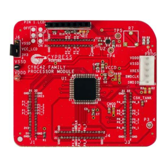
Fixed function digital blocks: Two combination UART/SPI/I2C (one function at a time) Serial Com- ■ munication Blocks (SCB). Four 16-bit Counter/Timer/PWMs with centre-aligned capability. CY8CKIT-038 PSoC 4200 Family Processor Module Kit Guide, Doc. # 001-85916 Rev. **... - Page 18 LCD drive on all pins Clocking: Trimmed IMO and ILO clock sources. ■ ■ Deep Sleep, Hibernate, and Stop low power modes Figure 4-2. CY8CKIT-038 PSoC 4200 Family Processor Module Board CY8CKIT-038 PSoC 4200 Family Processor Module Kit Guide, Doc. # 001-85916 Rev. **...
- Page 19 Hardware The CY8CKIT-038 PSoC 4200 family processor module board has the following four blocks: 44-Pin TQFP package PSoC 4200 family device ■ Four 2 × 16 headers, which connect to the CY8CKIT-001 DVK Main Board ■ CMOD circuitry for CapSense application ■...
- Page 20 Hardware CY8CKIT-038 PSoC 4200 Family Processor Module Kit Guide, Doc. # 001-85916 Rev. **...
-
Page 21: Example Projects
SAR ADC configured for a 12-bit operation; the ADC range is 0 to VDDA. The results are displayed on the I2C character LCD. Figure 5-1. Schematic and Flow Diagram of VoltageDisplay_SAR_ADC CY8CKIT-038 PSoC 4200 Family Processor Module Kit Guide, Doc. # 001-85916 Rev. **... - Page 22 Example Projects CY8CKIT-038 PSoC 4200 Family Processor Module Kit Guide, Doc. # 001-85916 Rev. **...
-
Page 23: Hardware Connections
Because it uses the potentiometer, the jumper VR_PWR (J11) should be in place. This connects the potentiometer to the VDDA. Connect the output of the VR pin to P2[7] (Voltage_Input) input pin as shown in Figure 5-3 on page CY8CKIT-038 PSoC 4200 Family Processor Module Kit Guide, Doc. # 001-85916 Rev. **... -
Page 24: Sar Adc Configuration
When the VDDA jumper on the board is set to 5 V, set Operating Conditions in the System tab to 5 V as shown in the following screenshot. CY8CKIT-038 PSoC 4200 Family Processor Module Kit Guide, Doc. # 001-85916 Rev. **... -
Page 25: Verify Output
ADC input is measured against internal VSSA. Any offset in the measurement can be positive or negative. This can result in a small offset voltage even when the potentiometer is zero. CY8CKIT-038 PSoC 4200 Family Processor Module Kit Guide, Doc. # 001-85916 Rev. **... -
Page 26: Project: Intensityled
PWM varies, the LED brightness changes. By continuously varying the pulse width of the PWM, the example code makes an LED go from low brightness to a high brightness and back. Figure 5-4. Intensity LED Project Flow Diagram CY8CKIT-038 PSoC 4200 Family Processor Module Kit Guide, Doc. # 001-85916 Rev. **... -
Page 27: Hardware Connections
Physical Connections on CY8CKIT-001 DVK Connect the output pin P1[5] (LED) to any one of the LEDs present on the CY8CKIT-001 DVK as shown in Figure 5-5. CY8CKIT-038 PSoC 4200 Family Processor Module Kit Guide, Doc. # 001-85916 Rev. **... -
Page 28: Verify Output
Reset button or power cycling the board. The project output is LED1 glowing with a brightness con- trol that changes with time. Figure 5-5. IntensityLED Project Demonstration CY8CKIT-038 PSoC 4200 Family Processor Module Kit Guide, Doc. # 001-85916 Rev. **... -
Page 29: Project: Lowpowerdemo
Figure 5-6. LowPowerDemo Schematic and Flow diagram CY8CKIT-038 PSoC 4200 Family Processor Module Kit Guide, Doc. # 001-85916 Rev. **... - Page 30 Switch off the LED Turn off the LCD display Put the system into sleep Switch press? Wake up the system Turn on the LCD display Switch on the LED CY8CKIT-038 PSoC 4200 Family Processor Module Kit Guide, Doc. # 001-85916 Rev. **...
-
Page 31: Hardware Connections
■ LED is in ON state. When P1[6] (SwitchPin) is pressed, the LCD display turns off, LED turns off, and finally, the ■ device goes to sleep. CY8CKIT-038 PSoC 4200 Family Processor Module Kit Guide, Doc. # 001-85916 Rev. **... - Page 32 When P1[6] (SwitchPin) is pressed the second time, the device returns to Active mode and the ■ LCD display turns on and LED turns on. Figure 5-7. a) LowPowerDemo Project Demonstration (Active Mode) CY8CKIT-038 PSoC 4200 Family Processor Module Kit Guide, Doc. # 001-85916 Rev. **...
- Page 33 Example Projects Figure 5-7. b) LowPowerDemo Project Demonstration (Low Power Mode) LCD display is off LED is off CY8CKIT-038 PSoC 4200 Family Processor Module Kit Guide, Doc. # 001-85916 Rev. **...
-
Page 34: Project: Capsense
The example uses two CapSense buttons and one 5-element slider provided on the board. Each capacitive sensor on the board is scanned using the Cypress CSD algorithm. The but- tons are pre-tuned in the example code to take care of factors such as board parasitic. -
Page 35: Hardware Connections
The I2C character LCD and CapSense configurations are shown in the following table. Pin Name Port Name Reset P3[5] SCB_SCL P4[0] SCB_SDA P4[1] Button0 P0[5] Button1 P0[6] Slider0 P0[0] Slider1 P0[1] Slider2 P0[2] Slider3 P0[3] Slider4 P0[4] CY8CKIT-038 PSoC 4200 Family Processor Module Kit Guide, Doc. # 001-85916 Rev. **... -
Page 36: Connections In Psoc Creator (Capsense.cydwr File)
"ON" or "OFF". The LCD also shows the slider touch position as a percentage. When you touch a button, the LCD displays ON; when you remove the finger from the button, the LCD displays OFF as shown in Figure 5-9. CY8CKIT-038 PSoC 4200 Family Processor Module Kit Guide, Doc. # 001-85916 Rev. **... - Page 37 PSoC 4200 Family Processor Module. Example projects using the Character LCD are not provided with this kit. To use the Character LCD, move jumper J12 on CY8CKIT-001 to LCD Power ON. CY8CKIT-038 PSoC 4200 Family Processor Module Kit Guide, Doc. # 001-85916 Rev. **...
- Page 38 Example Projects CY8CKIT-038 PSoC 4200 Family Processor Module Kit Guide, Doc. # 001-85916 Rev. **...
-
Page 39: Appendix
Header 2x16 CY8CKIT-038 44 PIN TQFP CY8CKIT-038 44 PIN TQFP CY8CKIT-038 44 PIN TQFP Header 2x16 Size Size Size Document Number Document Number Document Number 630-60048-01 630-60048-01 630-60048-01 CY8CKIT-038 PSoC 4200 Family Processor Module Kit Guide, Doc. # 001-85916 Rev. **... -
Page 40: Bill Of Materials (Bom)
NO LOAD RES NO LOAD 0603 SMD Panasonic - ECG ERJ-3GEY0R00V Trimmer Resistors - Through Hole 10 K POT Bourns 3352T-1-103LF 3/8" round 10 Kohms 0.5 watt 20% CY8CKIT-038 PSoC 4200 Family Processor Module Kit Guide, Doc. # 001-85916 Rev. **... -
Page 41: Pin Assignment Table
GPIO,LCD,CSD,SCB1,PWM P3[1] GPIO,LCD,CSD,SCB1,PWM P3[2] GPIO,LCD,CSD,SCB1,PWM,SWD P3[3] GPIO,LCD,CSD,SCB1,PWM,SWD PORT 3 P3[4] GPIO,LCD,CSD,SCB1,PWM P3[5] GPIO,LCD,CSD,SCB1,PWM P3[6] GPIO,LCD,CSD,SCB1,PWM P3[7] GPIO,LCD,CSD,PWM P4[0] GPIO,LCD,CSD,SCB0 P4[1] GPIO,LCD,CSD,SCB0 PORT 4 P4[2] GPIO,LCD,CSD,SCB0 P4[3] GPIO,LCD,CSD,SCB0 CY8CKIT-038 PSoC 4200 Family Processor Module Kit Guide, Doc. # 001-85916 Rev. **... -
Page 42: Regulatory Compliance Information
ANALOG SUPPLY (1.8-5.5V) VSSA ANALOG GROUND DIGITAL GROUND Regulatory Compliance Information CY8CKIT-038 has been tested and verified to comply with the following electromagnetic compatibil- ity (EMC) regulations: EN 55022:2010 Class A - Emissions ■ EN 55024:2010 Class A - Immunity ■...
Need help?
Do you have a question about the CY8CKIT-038 and is the answer not in the manual?
Questions and answers