Table of Contents
Advertisement
Quick Links
This user's guide describes the functionality, hardware, operation, and software instructions for the
TSW14J10 FMC-USB interposer card. Throughout this document, the abbreviations TSW14J10EVM,
EVM, and the term evaluation module are synonymous with the TSW14J10 Evaluation Module, unless
otherwise noted.
...................................................................................................................
1
2
3
3.1
3.2
3.3
4
4.1
4.2
5
6
6.1
6.2
6.3
6.4
6.5
1
2
3
4
5
6
7
8
9
10
11
12
13
14
15
16
17
18
Altera is a registered trademark of Altera Corporation.
Xilinx, Kintex are registered trademarks of Xilinx Corporation.
SLAU580B - June 2014 - Revised September 2016
Submit Documentation Feedback
TSW14J10 FMC-USB Interposer Card
..................................................................................................................
.....................................................................................................
................................................................................................
..............................................................................................................
..........................................................................................................
............................................................................................................
.............................................................................................
.......................................................................................
.........................................................................................
...........................................................................................
...............................................................................................................
..........................................................................................
...............................................................................................
....................................................................................
...........................................................................................................
.........................................................................................
.........................................................................................
.............................................................................................................
..................................................................................
.............................................................................................................
.........................................................................................
Copyright © 2014-2016, Texas Instruments Incorporated
SLAU580B - June 2014 - Revised September 2016
Contents
List of Figures
.......................................................................
....................................................................
...............................................................
.......................................................................
...............................................................
TSW14J10 FMC-USB Interposer Card
User's Guide
..................
..................................
...............................
..............................
......................
.........................
.........................................
2
2
4
4
4
5
9
9
11
13
15
16
21
25
30
32
3
4
9
11
11
12
16
17
18
19
20
20
21
22
23
23
24
25
1
Advertisement
Table of Contents

Related Manuals for Texas Instruments TSW14J10


Summary of Contents for Texas Instruments TSW14J10
-
Page 1: Table Of Contents
This user's guide describes the functionality, hardware, operation, and software instructions for the TSW14J10 FMC-USB interposer card. Throughout this document, the abbreviations TSW14J10EVM, EVM, and the term evaluation module are synonymous with the TSW14J10 Evaluation Module, unless otherwise noted. Contents ........................ -
Page 2: Introduction
(see Table The TSW14J10 routes the SPI busses through level translators that allow the signals going to the FPGA development board and the ADC/DAC EVM to be either 3.3-V or 1.8-V levels. All devices on the TSW14J10 are powered from the USB connection. -
Page 3: Tsw14J10Evm, Ads42Jb69Evm, And Kintex Kc705 Development Card
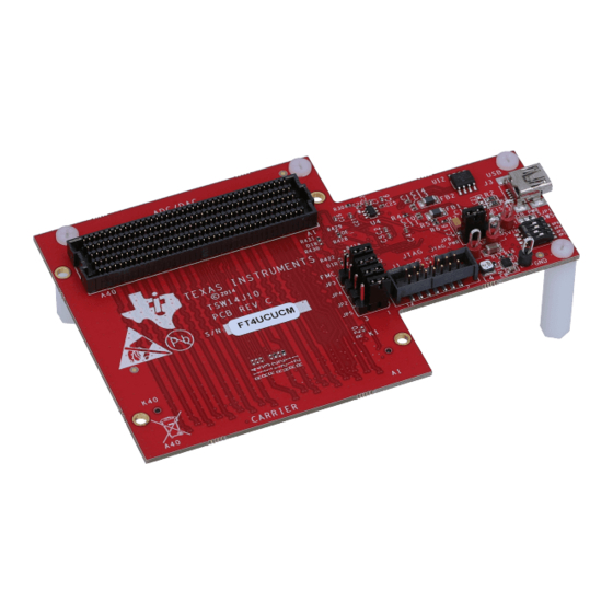
Functionality www.ti.com Figure 1. TSW14J10EVM, ADS42JB69EVM, and Kintex KC705 Development Card The major features of the TSW14J10 are: • 10 transceiver lanes with speeds up to 12.5 Gbps • Industry-standard JTAG connector • Supports 1.8-V, 3.3-V CMOS IO interface •... -
Page 4: Hardware Configuration
TP12. The external source should be able to provided 0.5 A. Jumpers The TSW14J10 contains several jumpers (JP) and solder jumpers (SJP) that enable certain functions on the board. The description of the jumpers are found in Table 1. -
Page 5: Connectors
FPGA Development Platform FMC Connector The TSW14J10 EVM has one FPGA Mezzanine Card Connector (FMC) to allow for direct plug in of a TI JESD204B serial interface ADC or DAC EVM and another to plug into an FPGA development board. The specifications for this connector were mostly derived from the ANSI/VITA 57.1 FPGA Mezzanine Card... - Page 6 Hardware Configuration www.ti.com Table 2. FPGA FMC Connector (J5) Description of the TSW14J10 (continued) CLK_LA0_P/N G6/G7 DEVCLKB+/- (M->C) Secondary carrier-bound device clock. Used for special FPGA functions such as sampling SYSREF. D8/D9 D8/D9 DEVCLK+/- (C->M) Mezzanine-bound device Clock. Used for low noise conversion clock.
- Page 7 Hardware Configuration www.ti.com Table 2. FPGA FMC Connector (J5) Description of the TSW14J10 (continued) Spare connection Spare connection Spare connection Spare connection 3.3.2 ADC/DAC FMC Connector FMC connector J4 provides the interface between the TSW14J10EVM and an ADC or DAC EVM. In addition to the JESD204B standard signals, 8 CMOS single-ended signals are sourced from the USB interface to the FMC connector.
- Page 8 USB interface device. This interface allows the HSDC Pro GUI the capability to configure an FPGA on a development platform if it has a corresponding JTAG connector that is routed directly to the FPGA JTAG pins. Connect the provide JTAG cable between the TSW14J10 JTAG connector and the FPGA development board JTAG connector.
-
Page 9: Software Start Up
Next one last time. The installation is now complete. The GUI executable and associated files will reside in the following directory. "C:\Program Files (x86)\Texas Instruments\High Speed Data Converter Pro" SLAU580B – June 2014 – Revised September 2016 TSW14J10 FMC-USB Interposer Card Submit Documentation Feedback Copyright ©... - Page 10 GUI version and will not work for a GUI version that the patch was not explicitly created for. TSW14J10 FMC-USB Interposer Card SLAU580B – June 2014 – Revised September 2016 Submit Documentation Feedback Copyright © 2014–2016, Texas Instruments Incorporated...
-
Page 11: Usb Interface And Drivers
4. It is possible to connect several TSW14J10 EVMs to one host PC but the GUI can only connect to one at a time. In the case where multiple boards are connected to the PC, the pop-up will display all of the serial numbers found. The user then selects which board the GUI will be associated with. -
Page 12: Hardware Device Manager
When the software is installed and the USB cable has been connected to the TSW14J10EVM and the PC, the TSW14J10 USB serial converter should be located in the Hardware Device Manager under the Universal Serial Bus controllers as shown in Figure 6. -
Page 13: Downloading Firmware Example
If the FPGA development platform is to be programmed using the TSW14J10EVM, either connect the provided ribbon cable between the TSW14J10 JTAG connector and the FPGA development platform JTAG connector or move the shunts on JP2–JP5 to pins 2-3 if the JTAG signals are routed to the FMC connector. - Page 14 EVM, consult the High Speed Data Converter Pro GUI User’s Guide (SLWU087) along with the individual EVM User’s Guide. TSW14J10 FMC-USB Interposer Card SLAU580B – June 2014 – Revised September 2016 Submit Documentation Feedback Copyright © 2014–2016, Texas Instruments Incorporated...
-
Page 15: Dac And Adc Gui Configuration File Changes When Using A Xilinx Development Platform
4 and the highest value that can be entered for number of samples in HSDC Pro GUI will be 64K. SLAU580B – June 2014 – Revised September 2016 TSW14J10 FMC-USB Interposer Card Submit Documentation Feedback Copyright © 2014–2016, Texas Instruments Incorporated... -
Page 16: Dac38J84Evm With Xilinx Vc707 Development Board Setup Example
3. Connect the power cables to the VC707 and DAC38J84. 4. Connect a USB cable between the TSW14J10 and a host computer with the HSDC Pro GUI loaded. 5. Connect a USB cable between the DAC38J84 and a host computer with the DAC3XJ8X GUI loaded. -
Page 17: Quick Start Menu
Click on the Program LMK04828 and DAC3XJ8X button. After the programming has completed, click on the LMK04828 Controls tab. Next, click on the Clock Outputs tab. SLAU580B – June 2014 – Revised September 2016 TSW14J10 FMC-USB Interposer Card Submit Documentation Feedback Copyright © 2014–2016, Texas Instruments Incorporated... -
Page 18: Lmk04828 Clock Outputs Menu
To generate a Core clock of 184.32 MHz, set the DCLK Divider for CLKout 12 to “16”. Also, remove the checkmark from the Group Powerdown box to enable this output. TSW14J10 FMC-USB Interposer Card SLAU580B – June 2014 – Revised September 2016 Submit Documentation Feedback Copyright © 2014–2016, Texas Instruments Incorporated... -
Page 19: Lmk04828 Clock Outputs Menu
DAC and ADC GUI Configuration File Changes When Using a Xilinx Development Platform www.ti.com The Clock Outputs menu is now as shown in Figure Figure 10. LMK04828 Clock Outputs Menu SLAU580B – June 2014 – Revised September 2016 TSW14J10 FMC-USB Interposer Card Submit Documentation Feedback Copyright © 2014–2016, Texas Instruments Incorporated... -
Page 20: Hsdc Pro Gui
Go back to the DAC GUI Quick Start tab and click the Reset DAC JESD Core button. Click on Trigger LMK04828 SYSREF. There should now be a 10-MHz tone present at all four DAC EVM outputs. TSW14J10 FMC-USB Interposer Card SLAU580B – June 2014 – Revised September 2016 Submit Documentation Feedback Copyright © 2014–2016, Texas Instruments Incorporated... -
Page 21: Adc32Rf45Evm With Xilinx Vc707 Development Board Setup Example
3. Connect the power cables to the VC707 and ADC32RF45. 4. Connect a USB cable between the TSW14J10 and a host computer with HSDC Pro GUI loaded. 5. Connect a USB cable between the ADC32RF45 and a host computer with ADC32RFxx GUI loaded. -
Page 22: Adc32Rfxx Gui Lmk0828 Clock Outputs Tab
= 200 MHz, set the DCLK Divider to 10 for CLKout 12 and unselect the Group Powerdown option for this clock. The GUI will now appear as shown in Figure TSW14J10 FMC-USB Interposer Card SLAU580B – June 2014 – Revised September 2016 Submit Documentation Feedback Copyright © 2014–2016, Texas Instruments Incorporated... -
Page 23: Updated Lmk0828 Clock Outputs Tab
16. Click the OK button. Figure 16. HSDC Pro GUI Click the Capture button. The captured results should look as shown in Figure SLAU580B – June 2014 – Revised September 2016 TSW14J10 FMC-USB Interposer Card Submit Documentation Feedback Copyright © 2014–2016, Texas Instruments Incorporated... -
Page 24: Captured Results For Channel A
DAC and ADC GUI Configuration File Changes When Using a Xilinx Development Platform www.ti.com Figure 17. Captured Results for Channel A TSW14J10 FMC-USB Interposer Card SLAU580B – June 2014 – Revised September 2016 Submit Documentation Feedback Copyright © 2014–2016, Texas Instruments Incorporated... -
Page 25: Adc12J4000Evm With Xilinx Vc707 Development Board Setup Example
Use the ADC12J4000EVM GUI A, shown in Figure 19, and follow steps 3.4–3.9 and 3.11 in the ADC12J4000EVM User’s Guide to configure the ADC EVM. SLAU580B – June 2014 – Revised September 2016 TSW14J10 FMC-USB Interposer Card Submit Documentation Feedback Copyright © 2014–2016, Texas Instruments Incorporated... - Page 26 3. Go to address 0x100, do a Read Register and verify the value “A” is read back. If not, write this value to this address. TSW14J10 FMC-USB Interposer Card SLAU580B – June 2014 – Revised September 2016 Submit Documentation Feedback Copyright © 2014–2016, Texas Instruments Incorporated...
- Page 27 DAC and ADC GUI Configuration File Changes When Using a Xilinx Development Platform www.ti.com Figure 20. LMK04828 Address 0x100 SLAU580B – June 2014 – Revised September 2016 TSW14J10 FMC-USB Interposer Card Submit Documentation Feedback Copyright © 2014–2016, Texas Instruments Incorporated...
- Page 28 The GUI will display the new lane rate and JESD reference clock required by the capture platform FPGA, as shown in Figure Click the OK button. Figure 22. HSDC Pro GUI TSW14J10 FMC-USB Interposer Card SLAU580B – June 2014 – Revised September 2016 Submit Documentation Feedback Copyright © 2014–2016, Texas Instruments Incorporated...
- Page 29 The captured results appear as shown in Figure Figure 23. Captured Results for the ADC12J4000 in Bypass Mode SLAU580B – June 2014 – Revised September 2016 TSW14J10 FMC-USB Interposer Card Submit Documentation Feedback Copyright © 2014–2016, Texas Instruments Incorporated...
-
Page 30: Adc12J4000Evm With A Xilinx Zynq Zc706 Development Board Setup Example
4. Connect a micro USB cable between J1 of the ZC706 and a host computer with Vivado loaded. 5. Connect a USB cable between the TSW14J10 and a host computer with HSDC Pro GUI loaded. 6. Connect a USB cable between the ADC12J4000 and a host computer with ADC12J4000 GUI loaded. - Page 31 11. A new window will open showing the status of the programming. Once this reached 100%, the FPGA is programmed and ready to be used with the TSW14J10 to run the HSDC Pro GUI. Open the HSDC Pro GUI, select the ADC tab, then select “ADC12J4000_BYPASS” using the device drop- down arrow.
-
Page 32: Dac38J84Evm With A Xilinx Zynq Zc706 Development Board Setup Example
The first step is to program the DAC38J84EVM which will provide the reference and core clocks to the ZC706. 1. Connect the TSW14J10 to FMC HPC connector J37 on the ZC706. 2. Connect the DAC to the other end of the TSW14J10. - Page 33 4. Connect a micro USB cable between J1 of the ZC706 and a host computer with Vivado loaded. 5. Connect a USB cable between the TSW14J10 and a host computer with HSDC Pro GUI loaded. 6. Connect a USB cable between the DAC38J84 and a host computer with DAC3XJ8X GUI loaded.
- Page 34 Click on “Trigger LMK04828 SYSREF”. There should now be a 10-MHz tone present at all four DAC EVM outputs. Other EVM’s that have tested with the ZC706 platform include the ADS42JB49/69, ADC32RF45, and DAC38J84. TSW14J10 FMC-USB Interposer Card SLAU580B – June 2014 – Revised September 2016 Submit Documentation Feedback Copyright © 2014–2016, Texas Instruments Incorporated...
- Page 35 Added the ADC12J4000EVM With a Xilinx Zynq ZC706 Development Board Setup Example section ......• Added the DAC38J84EVM With a Xilinx Zynq ZC706 Development Board Setup Example section. SLAU580B – June 2014 – Revised September 2016 Revision History Submit Documentation Feedback Copyright © 2014–2016, Texas Instruments Incorporated...
- Page 36 STANDARD TERMS AND CONDITIONS FOR EVALUATION MODULES Delivery: TI delivers TI evaluation boards, kits, or modules, including demonstration software, components, and/or documentation which may be provided together or separately (collectively, an “EVM” or “EVMs”) to the User (“User”) in accordance with the terms and conditions set forth herein.
- Page 37 FCC Interference Statement for Class B EVM devices NOTE: This equipment has been tested and found to comply with the limits for a Class B digital device, pursuant to part 15 of the FCC Rules. These limits are designed to provide reasonable protection against harmful interference in a residential installation.
- Page 38 【無線電波を送信する製品の開発キットをお使いになる際の注意事項】 開発キットの中には技術基準適合証明を受けて いないものがあります。 技術適合証明を受けていないもののご使用に際しては、電波法遵守のため、以下のいずれかの 措置を取っていただく必要がありますのでご注意ください。 1. 電波法施行規則第6条第1項第1号に基づく平成18年3月28日総務省告示第173号で定められた電波暗室等の試験設備でご使用 いただく。 2. 実験局の免許を取得後ご使用いただく。 3. 技術基準適合証明を取得後ご使用いただく。 なお、本製品は、上記の「ご使用にあたっての注意」を譲渡先、移転先に通知しない限り、譲渡、移転できないものとします。 上記を遵守頂けない場合は、電波法の罰則が適用される可能性があることをご留意ください。 日本テキサス・イ ンスツルメンツ株式会社 東京都新宿区西新宿6丁目24番1号 西新宿三井ビル 3.3.3 Notice for EVMs for Power Line Communication: Please see http://www.tij.co.jp/lsds/ti_ja/general/eStore/notice_02.page 電力線搬送波通信についての開発キットをお使いになる際の注意事項については、次のところをご覧ください。http:/ /www.tij.co.jp/lsds/ti_ja/general/eStore/notice_02.page SPACER EVM Use Restrictions and Warnings: 4.1 EVMS ARE NOT FOR USE IN FUNCTIONAL SAFETY AND/OR SAFETY CRITICAL EVALUATIONS, INCLUDING BUT NOT LIMITED TO EVALUATIONS OF LIFE SUPPORT APPLICATIONS.
- Page 39 Notwithstanding the foregoing, any judgment may be enforced in any United States or foreign court, and TI may seek injunctive relief in any United States or foreign court. Mailing Address: Texas Instruments, Post Office Box 655303, Dallas, Texas 75265 Copyright © 2016, Texas Instruments Incorporated...
- Page 40 IMPORTANT NOTICE Texas Instruments Incorporated and its subsidiaries (TI) reserve the right to make corrections, enhancements, improvements and other changes to its semiconductor products and services per JESD46, latest issue, and to discontinue any product or service per JESD48, latest issue.
- Page 41 Mouser Electronics Authorized Distributor Click to View Pricing, Inventory, Delivery & Lifecycle Information: Texas Instruments TSW14J10EVM...
Need help?
Do you have a question about the TSW14J10 and is the answer not in the manual?
Questions and answers