Table of Contents
Advertisement
Quick Links
All manuals and user guides at all-guides.com
UM1935
User manual
Evaluation board with STM32F479NI MCU
Introduction
The STM32479I-EVAL evaluation board is a complete demonstration and development
®
®
platform for STMicroelectronics ARM
Cortex
-M4 core-based STM32F479NIH6
2
2
microcontroller. It features three I
C, six SPIs with two multiplexed full-duplex I
S interfaces,
SDMMC, four USARTs and four UARTs, two CANs, three 12-bit ADCs, two 12-bit DACs,
one SAI, 8 to 14-bit digital camera module interface, internal 320+4 Kbytes of SRAM and 2
Mbytes of Flash memory, USB HS OTG and USB FS OTG, Ethernet MAC, FMC interface,
MIPI DSI interface, Quad-SPI interface, Cryptographic acceleration, JTAG and ETM
debugging support. This evaluation board can be used as a reference design for user
application development but it cannot be considered as a final application.
The full range of hardware features on the board helps the user to evaluate all peripherals
(USB OTG HS, USB OTG FS, Ethernet, motor control, CAN, microSD Card, USART, Audio
DAC and ADC, digital microphone, IrDA, RF-EEPROM, SRAM, NOR Flash, SDRAM,
Quad-SPI Flash, 4" TFT LCD with MIPI DSI interface and capacitive touch panel and
others) and to develop his own applications. Extension headers make it possible to easily
connect a daughterboard for specific application.
The integrated ST-LINK/V2-1 provides an embedded in-circuit debugger and programmer
for the STM32 MCU.
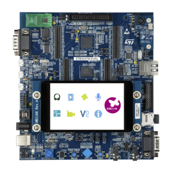
Figure 1. STM32479I-EVAL evaluation board
1. Picture not contractual.
September 2015
DocID028194 Rev 1
1/77
www.st.com
1
Advertisement
Table of Contents

Related Manuals for ST UM1935


Summary of Contents for ST UM1935
- Page 1 Quad-SPI Flash, 4" TFT LCD with MIPI DSI interface and capacitive touch panel and others) and to develop his own applications. Extension headers make it possible to easily connect a daughterboard for specific application. The integrated ST-LINK/V2-1 provides an embedded in-circuit debugger and programmer for the STM32 MCU. Figure 1. STM32479I-EVAL evaluation board 1.
-
Page 2: Table Of Contents
Embedded ST-LINK/V2-1 ........11... - Page 3 MFX programming connector CN21 ......46 6.19 ST-LINK/V2-1 USB type B connector CN22 ..... . . 46 6.20 CAN D-type 9-pins male connector CN23 .
- Page 4 All manuals and user guides at all-guides.com List of tables UM1935 List of tables Table 1. Power related jumpers ........... . 14 Table 2.
- Page 5 ST-LINK/V2-1 ........
-
Page 6: Features
STM32F479NIH6 microcontroller with 2 Mbytes of Flash memory and 320+4 Kbytes of RAM in TFBGA package Six 5 V power supply options: – Power jack – ST-LINK/V2-1 USB connector – User USB HS connector – User USB FS1 connector – User USB FS2 connector –... -
Page 7: Demonstration Software
For more information and to download the latest version available, refer to the STM32479I-EVAL demonstration software available on www.st.com. Order code To order the STM32479I-EVAL evaluation board, based on the STM32F479NI MCU, use the order code STM32479I-EVAL. -
Page 8: Hardware Layout And Configuration
STM32F479NIH6 and peripherals (SDRAM, SRAM, NOR Flash, QSPI Flash, Camera module, Color LCD, USB OTG connectors, motor control connector, USART, IrDA, Ethernet, Audio, CAN, RF-EEPROM, microSD card and embedded ST-LINK) and Figure 3: STM32479I-EVAL evaluation board layout will help to locate these features on the actual evaluation board. -
Page 9: Figure 2. Hardware Block Diagram
All manuals and user guides at all-guides.com UM1935 Hardware Layout and configuration Figure 2. Hardware Block Diagram 1. The circles show the I/O shared with motor control. DocID028194 Rev 1 9/77... -
Page 10: Figure 3. Stm32479I-Eval Evaluation Board Layout
All manuals and user guides at all-guides.com Hardware Layout and configuration UM1935 Figure 3. STM32479I-EVAL evaluation board layout RF EEPROM daughter board IrDA Motor control connector connector CN5,CN6 Camera Extension extension header connector STM32F756NGH6 CN12 ETM TRACE USART1 CN25 CN10,CN11... -
Page 11: Embedded St-Link/V2-1
V2 and V2-1 refer to ST-LINK/V2 User Manual UM1075. Note 1: It is possible to power the board via CN22 (Embedded ST-LINK/V2-1 USB connector) even if an external tools is connected to CN12 (ETM Trace connector) or CN16 (External JTAG and SWD connector). -
Page 12: St-Link/V2-1 Firmware Upgrade
The ST-LINK/V2-1 embeds a firmware upgrade mechanism for in-situ upgrade through the USB port. As the firmware may evolve during the life time of the ST-LINK/V2-1 product (for example new functionality, bug fixes, support for new microcontroller families), it is recommended to visit www.st.com... -
Page 13: Table 1. Power Related Jumpers
All manuals and user guides at all-guides.com UM1935 Hardware Layout and configuration required power, the enumeration succeeds, the power transistor U18 (ST890) is switched ON, the red LED LD10 is turned ON, thus STM32479I-EVAL board is powered and can consume maximum 300mA current, but not more. If the host is not able to provide the requested current, the enumeration fails. - Page 14 JP10 is set as shown to the right: JP14 is used to select one of the six possible power supply resources. For power supply from USB connector of ST-LINK/V2-1 (CN22) to STM32479I- EVAL only, JP14 is set as shown to the right:...
-
Page 15: Clock Source
All manuals and user guides at all-guides.com UM1935 Hardware Layout and configuration Table 1. Power related jumpers (continued) Jumper Description For power supply from USB OTG1 FS (CN13) to only, STM32479I-EVAL JP14 is set as shown to the right: For power supply from USB OTG2 HS (CN8) to... -
Page 16: Reset Source
All manuals and user guides at all-guides.com Hardware Layout and configuration UM1935 Table 2. 25MHz Crystal X1 related solder bridges Jumper Description PH0 is connected to 25MHz crystal when SB37 is open. (Default setting) SB37 PH0 is connected to extension connector CN5 when SB37 is closed. In such case R20 must be removed to avoid disturbance due to the 25MHz quartz PH1 is connected to 25MHz crystal when SB38 is open. -
Page 17: Boot Option
All manuals and user guides at all-guides.com UM1935 Hardware Layout and configuration Boot option STM32479I-EVAL evaluation board can boot from: Embedded User Flash System memory with boot loader for ISP Embedded SRAM for debugging The boot option is configured by setting switch SW1 (BOOT0) and SW2 (BOOT1). The BOOT0 can be configured also via RS232 connector CN7. -
Page 18: Table 6. Audio Related Jumpers
All manuals and user guides at all-guides.com Hardware Layout and configuration UM1935 The analog microphone on the headset is connected to ADC of WM8994ECS/R through audio jack CN27. External speakers can be connected to WM8994ECS/R via audio jack CN26. Two digital microphones (MEMS microphone) MP34DT01TR are on STM32479I-EVAL evaluation board. -
Page 19: Usb Otg1 Fs
All manuals and user guides at all-guides.com UM1935 Hardware Layout and configuration Table 6. Audio related jumpers (continued) Jumper Description PD6 is as FMC_NWAIT signal when JP6 is set as shown to the right (Default setting): PD6 is connected to digital microphone as I... -
Page 20: Usb Otg2 Hs And Fs
IrDA transceiver U1, which is connected to USART1 of STM32F479NIH6 on STM32479I- EVAL evaluation board. The signals Bootloader_RESET and Bootloader_BOOT0 are added on RS232 connector CN7 for ISP support. USART1 of STM32F479NIH6 is shared with RS232/IrDA and ST-LINK/V2-1 controller. Its communication can be changed by setting JP15 and JP19. 20/77... -
Page 21: Microsd Card
USART1_RX is connected to RS232/IrDA when JP15 is set as shown to the right (Default setting): JP15 USART1_RX is connected to ST-LINK/V2-1 controller’s USART_TX when JP15 is set as shown to the right: USART1_TX is connected to RS232/IrDA when JP19 is set as shown to the right... -
Page 22: Can
All manuals and user guides at all-guides.com Hardware Layout and configuration UM1935 5.12 STM32479I-EVAL evaluation board supports one channel of CAN2.0A/B compliant CAN bus communication based on 3.3V CAN transceiver. High-speed mode, standby mode and slope control mode are available and can be selected by setting JP12. -
Page 23: Memories
All manuals and user guides at all-guides.com UM1935 Hardware Layout and configuration Table 11. Ethernet related solder bridges Solder Description bridges MII CRS on DP83848CVV is connected to PA0 when SB48 is closed and SB44, SB46 are open SB48 Default setting: Open... -
Page 24: Quad-Spi Nor Flash
All manuals and user guides at all-guides.com Hardware Layout and configuration UM1935 By default, all these serial resistors are soldered on the board. If A18 is required, it is necessary to set (SAI_SDB) ADCDAT1 pin of audio codec WM8994ECS/R (U23) to be tri- state by software. -
Page 25: Camera Module
All manuals and user guides at all-guides.com UM1935 Hardware Layout and configuration 5.17 Camera module A connector CN4 for DCMI signals is on STM32479I-EVAL evaluation board and camera module daughterboard MB1183. DCMI signals are duplicated with other peripherals (SAI, I S, NOR Flash, microSD card, ETM, MEMS Microphone, potentiometer/PA4). -
Page 26: Motor Control
All manuals and user guides at all-guides.com Hardware Layout and configuration UM1935 Table 14. LCD modules connector (CN15) (continued) Pin No. Description Pin connection Pin No. Description Pin connection I2C1_SCL DSI_TE BL_CTRL DSI_RESET 5.19 Motor control STM32479I-EVAL evaluation board supports both asynchronous and synchronous three- phase brushless motor control via a 34 pins connector CN1, which provides all required control and feedback signals to and from motor power-driving board. -
Page 27: Figure 5. Stm32479I-Eval Evaluation Board Motor Control Pcb Reworks (Bottom Side)
All manuals and user guides at all-guides.com UM1935 Hardware Layout and configuration Figure 5. STM32479I-EVAL evaluation board motor control PCB reworks (bottom side) Figure 6. STM32479I-EVAL evaluation board motor control PCB reworks (top side) DocID028194 Rev 1 27/77... -
Page 28: Mfx (Multi Function Expander)
All manuals and user guides at all-guides.com Hardware Layout and configuration UM1935 Table 15. Motor control related solder bridges Solder Description bridges The motor current sampling operation is enabled when SB1 is closed (PA12 connected to PA8). The IO pins PA12 and PA8 are disconnected and can be used by daughterboard when SB1 is not fitted. - Page 29 All manuals and user guides at all-guides.com UM1935 Hardware Layout and configuration Table 16. MFX signals (continued) Direction Pin name of Function of Terminal number MFX function STM32479I-EVAL device (For MFX) of MFX MFX_GPIO3 JOY_RIGHT Input Joystick MFX_GPIO4 JOY_UP Input...
-
Page 30: Connectors
All manuals and user guides at all-guides.com Connectors UM1935 Connectors Motor control connector CN1 Figure 7. Motor control connector CN1 (top view) Table 17. Motor control connector CN1 Pin of Pin of Description number number Description STM32F479NIH6 STM32F479NIH6 of CN1... -
Page 31: Rf-Eeprom Daughterboard Connector Cn2
All manuals and user guides at all-guides.com UM1935 Connectors Table 17. Motor control connector CN1 (continued) Pin of Pin of Description number number Description STM32F479NIH6 STM32F479NIH6 of CN1 of CN1 Encoder A Encoder B Encoder Index RF-EEPROM daughterboard connector CN2 Figure 8. -
Page 32: Camera Module Connector Cn4
All manuals and user guides at all-guides.com Connectors UM1935 Table 19. Analog input-output connector CN3 Pin number Description Pin number Description analog input-output (PA4 or PC0) Table 13: Analog input related jumpers for details Camera module connector CN4 Figure 10. Camera module connector CN4 (top view) Table 20. -
Page 33: Daughterboard Extension Connectors Cn5 And Cn6
CN5 and CN6 and memory connectors CN10 and CN11. The space between these two connectors is defined as a standard which allows developing common daughterboards for several ST evaluation boards. The standard width between CN5 pin1 and CN6 pin1 is 2700mils (68.58mm). - Page 34 All manuals and user guides at all-guides.com Connectors UM1935 Table 21. Daughterboard extension connector CN5 (continued) How to disconnect function block on Description Alternative function STM32479I-EVAL board PB14 USB_FS2_DM/MC_VL open SB64, SB65 MII_RXD2/MC_DissipativeBrake open SB55, SB58 ULPI_D5/ PB12 open SB70, SB74, remove R254...
-
Page 35: Table 22. Daughterboard Extension Connector Cn6
All manuals and user guides at all-guides.com UM1935 Connectors Table 21. Daughterboard extension connector CN5 (continued) How to disconnect function block on Description Alternative function STM32479I-EVAL board MII_RXD3 remove R42 MII_RXD1/MC_HEATSINK open SB69, SB73 +3V3 ULPI_D1 open SB79 DSI_TE disconnect CN15 Table 22. - Page 36 All manuals and user guides at all-guides.com Connectors UM1935 Table 22. Daughterboard extension connector CN6 (continued) How to disconnect function block on Description Alternative Function STM32479I-EVAL board CAN1_RX/USB_FS1_DM open SB68, remove R281, leave JP9 open, PA11 /MC_PFCpwm disconnect CN13 RS232_IRDA_TX/USB_FS1_...
-
Page 37: Rs232 Connector Cn7
All manuals and user guides at all-guides.com UM1935 Connectors Table 22. Daughterboard extension connector CN6 (continued) How to disconnect function block on Description Alternative Function STM32479I-EVAL board CAN1_TX/USB_FS1_DP/MC PA12 open SB66, SB67, SB71 _PFCsync2 RS232_IRDA_RX/USB_FS1 PA10 remove R107, leave JP15 open... -
Page 38: Usb Otg2 Hs Micro-Ab Connector Cn8
All manuals and user guides at all-guides.com Connectors UM1935 USB OTG2 HS micro-AB connector CN8 Figure 12. USB OTG HS Micro-AB connector CN8 (front view) Table 24. USB OTG HS Micro-AB connector CN8 Pin number Description Pin number Description Ethernet RJ45 connector CN9 Figure 13. -
Page 39: Memory Connectors Cn10 And Cn11
The space between these two connectors is defined as a standard which allows to develop common daughterboards for several ST evaluation boards. The standard width between CN10 pin1 and CN11 pin1 is 1914mils (48.62mm). About details on assignment of the... - Page 40 All manuals and user guides at all-guides.com Connectors UM1935 Table 26. Memory connector CN10 (continued) How to disconnect function block on Description Alternative Function STM32479I-EVAL board PE11 PF15 PE14 PH10 A14/BA0 PH12 PD10 PD15 SDCLK/ MII_PPS_OUT Table 27. Memory connector CN11...
- Page 41 All manuals and user guides at all-guides.com UM1935 Connectors Table 27. Memory connector CN11 (continued) How to disconnect function block on Description Alternative Function STM32479I-EVAL board PH13 SDCKE0 A21/SAI1_SCK_A/TRACED2 open SB3, SB4, SB5 /PAR_D6 NWAIT /I2S3_SD/PAR_D10 set JP6 on pin1-2, disconnect CN4...
-
Page 42: Etm Trace Debugging Connector Cn12
All manuals and user guides at all-guides.com Connectors UM1935 6.10 ETM trace debugging connector CN12 Figure 14. ETM trace debugging connector CN12 (top view) Table 28. ETM trace debugging connector CN12 Pin number Description Description number +3.3V TMS/PA13 TCK/PA14 TDO/PB3... -
Page 43: Usb Otg2 Fs Micro-Ab Connector Cn14
All manuals and user guides at all-guides.com UM1935 Connectors Table 29. USB OTG1 FS Micro-AB connector CN13 Pin number Description Pin number Description (PA9) ID (PA10) D- (PA11) D+ (PA12) 6.12 USB OTG2 FS Micro-AB connector CN14 Figure 16. USB OTG FS1 Micro-AB connector CN13 (front view) Table 30. -
Page 44: Jtag/Swd Connector Cn16
All manuals and user guides at all-guides.com Connectors UM1935 6.14 JTAG/SWD connector CN16 Figure 17. JTAG/SWD debugging connector CN15 (top view) Table 31. JTAG/SWD debugging connector CN16 Pin number Description Description number +3.3V +3.3V PA15 PA13 PA14 RTCK RESET# DBGRQ... -
Page 45: Microsd Connector Cn17
All manuals and user guides at all-guides.com UM1935 Connectors 6.15 MicroSD connector CN17 Figure 18. MicroSD connector CN17 (top view) Table 32. MicroSD connector CN17 Description Description number number SDIO_D2 (PC10) Vss/GND SDIO_D3 (PC11) SDIO_D0 (PC8) SDIO_CMD (PD2) SDIO_D1 (PC9) +3.3V... -
Page 46: St-Link/V2-1 Programming Connector Cn20
It is not populated by default and not intended for end user. 6.19 ST-LINK/V2-1 USB type B connector CN22 The USB connector CN22 is used to connect embedded ST-LINK/V2-1 to PC for debugging of board. Figure 20. USB type B connector CN22 (front view) Table 33. -
Page 47: Can D-Type 9-Pins Male Connector Cn23
All manuals and user guides at all-guides.com UM1935 Connectors Table 33. USB type B connector CN22 (continued) Pin number Description Pin number Description Shield 6.20 CAN D-type 9-pins male connector CN23 Figure 21. RS232 connector CN23 (front view) Table 34. CAN D-type 9-pins male connector CN23... -
Page 48: Audio Jack (Speaker) Cn26
All manuals and user guides at all-guides.com Connectors UM1935 6.22 Audio jack (Speaker) CN26 A 3.5 mm stereo audio jack CN26 for speaker out is available on STM32479I-EVAL evaluation board to support external speaker. 6.23 Audio jack CN27 A 3.5 mm stereo audio jack CN27 is available on STM32479I-EVAL evaluation board to support headset (headphone and microphone integrated). -
Page 49: Schematics
All manuals and user guides at all-guides.com Schematics Figure 23. STM32F479I-EVAL evaluation board U_MCU MCU.SchDoc U_Memory R151 Same length Memory.SchDoc +3V3 I2C1_SCL R152 I2C1_SDA A[0..23] A[0..23] U_Audio D[0..31] D[0..31] Audio.SchDoc 90MHz clock SDCLK SDCLK I2C1_SCL SAI1_SCKA SAI1_SCKA SDNE0 SDNE0 I2C1_SDA SAI1_FSA SAI1_FSA SDNRAS... -
Page 50: Figure 24. Mcu
All manuals and user guides at all-guides.com Figure 24. MCU SB46 Open MC_EnA SB48 Open MII_CRS SB44 Closed WAKEUP SB33 Open MC_EnB SB39 Closed MII_RX_CLK Potentiometer_PC0 SB42 Open Closed SB34 MC_EnIndex ULPI_STP SB40 Closed Open SB41 MII_MDIO MC_CurrentA Closed SB31 Potentiometer_PA4 MII_MDC SB47... -
Page 51: Figure 25. Power
All manuals and user guides at all-guides.com Figure 25. Power ZEN056V130A24LS CN19 220uF DC-10B SMAJ5.0A-TR 100nF BNX002-01 +3V3 VDD_MCU C130 [N/A] C107 [N/A] [N/A] [N/A] JP14 VBUS_HS VBUS_FS1 TP14 TP13 TP16 +3V3 LD1117S18TR +1V8 VBUS_FS2 LD10 Ground Ground Ground Ground Vout R130 U5V_ST_LINK... -
Page 52: Figure 26. Sram, Flash And Sdram
All manuals and user guides at all-guides.com Figure 26. SRAM, FLASH and SDRAM D[0..31] D[0..31] A[0..23] A[0..23] DQ31 DQ30 I/O15 DQ15A-1 DQ29 I/O14 DQ14 DQ28 I/O13 DQ13 DQ27 I/O12 DQ12 DQ26 I/O11 DQ11 DQ25 I/O10 DQ10 DQ24 I/O9 DQ23 I/O8 DQ22 I/O7 DQ21... -
Page 53: Figure 27. Audio
All manuals and user guides at all-guides.com Figure 27. Audio +3V3 LDO1VDD AGND Default I2C Address:0011010 +3V3 AVDD1 AGND SPKVDD1 AGND +1V8 SPKVDD2 SPKGND1 AVDD2 SPKGND2 +1V8 CPVDD CPGND +3V3 DCVDD DGND DBVDD HP2GND +1V8 LDO2VDD R172 I2C1_SDA R171 R179 +3V3 LDO1ENA SCLK... -
Page 54: Figure 28. Lcd, Camera And Connectors
All manuals and user guides at all-guides.com Figure 28. LCD, camera and connectors CN15 DSI LCD Camera To MFX TOUCH_INT MFX_GPIO14 PAR_D[0..11] DSI_CK_P TOUCH_INT PAR_D[0..11] DSI_CK_N +1V8 C106 C105 DSI_D0_P DSI_D0_N 100nF 100nF DSI_D1_P +3V3 +1V8 DSI_D1_N PAR_D10 PAR_D11 R218 R220 R225 PC10... -
Page 55: Figure 29. Ethernet
All manuals and user guides at all-guides.com Figure 29. Ethernet +3V3 R118 100nF R110 R105 100nF MII_TX_CLK TX_CLK PG11 MII_TX_EN TX_EN PG13/PB12 MII_TXD0 TXD_0 PG14 MII_TXD1 TXD_1 MII_TXD2 TXD_2 MII_TXD3 TXD_3/SNI_MODE MII_RXD0 RXD_0/PHYAD1 MII_RXD1 RXD_1/PHYAD2 LED(green)_A MII_RXD2 RXD_2/PHYAD3 LED(green)_K MII_RXD3 RXD_3/PHYAD4 LED(Yellow)_A PI10... -
Page 56: Figure 30. Usb Otg Hs
All manuals and user guides at all-guides.com Figure 30. USB OTG HS +3V3 R122 CN14 PB13 VBUS_FS2 VBUS PB14 R284 USB_FS2_DM PB15 R283 USB_FS2_DP PB12 USB_FS2_ID Green Vbus D+out D+in Shield D-out D-in Shield R126 Shield 9013 Shield 475900001 R127 +3V3 EMIF02-USB03F2 R111... -
Page 57: Figure 31. Usb Otg Fs
All manuals and user guides at all-guides.com Figure 31. USB OTG FS +3V3 R120 MFX_GPIO6 OTG_FS1_OverCurrent R121 To MFX R119 CN13 FAULT VBUS MFX_GPIO7 R117 OTG_FS1_PowerSwitchOn From MFX STMPS2151STR 4.7uF R116 Shield Shield Shield Shield 475900001 +3V3 VBUS_FS1 PA11 R281 USB_FS1_DM PA12 R280... -
Page 58: Figure 32. Rs232 And Irda
All manuals and user guides at all-guides.com Figure 32. RS232 and IrDA +3V3 C138 C139 100nF 100nF DB9-male USART1 C137 100nF 100nF 100nF T1IN T1OUT RS232/IrDA_TX T2IN T2OUT T3IN T3OUT R1OUTB Bootloader_BOOT0 R2OUTB R1OUT R1IN R2OUT R2IN R3OUT R3IN PA10 RS232/IrDA_RX Bootloader_RESET R4OUT... -
Page 59: Figure 33. Can And Qspi
All manuals and user guides at all-guides.com Figure 33. CAN and QSPI +3V3 R173 R181 +3V3 CN23 C183 Default setting: 1<->2 DB9-male CAN connector Default setting: Open JP12 100nF PA12 JP13 CAN1_TX CANH CANL PA11 CAN1_RX Vref R175 SN65HVD230 ESDCAN24-2BLY R174 R176 Optional... -
Page 60: Figure 34. Peripherals
All manuals and user guides at all-guides.com Figure 34. Peripherals Buttons +3V3 Joystick COMMON COMMON COMMON +3V3 +3V3 Selection R207 R204 R203 PC13 To MFX TAMPER_KEY MFX_GPIO0 JOY_SEL WKUP MFX_GPIO1 C103 JOY_DOWN DWON [N/A] MFX_GPIO2 JOY_LEFT LEFT MFX_GPIO3 JOY_RIGHT RIGHT USER (Blue) C100 MFX_GPIO4... -
Page 61: Figure 35. Motor Control
All manuals and user guides at all-guides.com Figure 35. Motor control +3V3 Motor control connector MC_EmergencySTOP EMERGENCY STOP [N/A] MC_UH MC-UH MC_UL MC_UL MC_VH MC_VH PB14 MC_VL MC_VL MC_WH MC_WH PB15 MC_WL MC_WL BUS VOLTAGE MC_BusVoltage MC_CurrentA CURRENT A CURRENT B 100nF 100K CURRENT C... -
Page 62: Figure 36. Extension Connectors
All manuals and user guides at all-guides.com Figure 36. Extension connectors Place close Memory CN10 SDNE0 SDNWE PF13 PF14 PF12 PF11 SDNRAS Left Right SB37 PI11 PI13 SB36 SB35 11 12 Open SB38 PC15 PC14 PE10 13 14 R213 Open PI15 PC13 Open... -
Page 63: Figure 37. St-Link/V2-1
All manuals and user guides at all-guides.com Figure 37. ST-LINK/V2-1 VBUS_HS +3V3_ST_LINK BAT60JFILM R196 R195 VBUS_FS1 BAT60JFILM BAT60JFILM U17 LD3985M33R +3V3_ST_LINK C173 C175 C180 C178 JP20 VBUS_FS2 Vout 100nF 100nF 100nF 100nF +3V3_ST_LINK BAT60JFILM BYPASS R157 1uF_X5R_0603 1uF_X5R_0603 BAT60JFILM 100K... -
Page 64: Figure 38. Mfx
All manuals and user guides at all-guides.com Figure 38. MFX Multi Function eXpander +3V3 +3V3 +3V3 one capacitor close to each MFX pins: VDD, VDD_1, VDD_2, VDD_3 Ferrite C177 C182 C176 C174 C179 100nF 100nF 100nF 100nF 100nF 100nF +3V3 STM32L152CCT6 R154 GPIO0... -
Page 65: Figure 39. Jtag And Trace
All manuals and user guides at all-guides.com Figure 39. JTAG and trace +3V3 R129 R131 R123 R124 [N/A] [N/A] [N/A] [N/A] PA13 TMS/SWDIO PA14 TCK/SWCLK TDO/SWO PA15 R103 TRST RESET# R128 [N/A] Trace connector JTAG connector CN16 CN12 +3V3 JTAG +3V3 +3V3 R132... -
Page 66: Figure 40. 4 Inch Dsi Lcd Board
All manuals and user guides at all-guides.com Figure 40. 4 inch DSI LCD board BLGND HSSI_CLK_N HSSI_CLK_N HSSI_CLK_P HSSI_CLK_P HSSI_CLK_P HSSI_CLK_N HSSI_D0_N HSSI_D0_N HSSI_D0_P HSSI_D0_P HSSI_D0_P HSSI_D0_N HSSI_D1_N HSSI_D1_N HSSI_D1_P HSSI_D1_P HSSI_D1_P BLVDD HSSI_D1_N BLVDD RESX BEAD CABC CABC 4.7uH(1A) BLGND 4.7uF/50V Open... -
Page 67: Figure 41. Camera Module
All manuals and user guides at all-guides.com Figure 41. Camera module +1V8 100nF 100nF +2V8 11 12 13 14 15 16 Camera_RST 17 18 STANDBY EXTCLK 19 20 +2V8 +2V8 +2V8 21 22 Camera_CLK PAR_D0 PAR_D1 MCLK AVDD(2.8V) 23 24 PAR_PCLK [N/A] PAR_D2... -
Page 68: Appendix A Stm32479I-Eval I/O Assignment
All manuals and user guides at all-guides.com Appendix A STM32479I-EVAL I/O assignment UM1935 Appendix A STM32479I-EVAL I/O assignment Table 36. STM32479I-EVAL I/O assignment Camera Pin Name STM32479I-EVAL standard Motor control variant variant A20 || TRACED1 || SAI1_FS_A A19 || TRACED0 ||... - Page 69 All manuals and user guides at all-guides.com UM1935 Appendix A STM32479I-EVAL I/O assignment Table 36. STM32479I-EVAL I/O assignment (continued) Camera Pin Name STM32479I-EVAL standard Motor control variant variant NWAIT || MICROPHONE2_I2S3_MOSI /3_SD PC11 SDCARD_D3 || SPI3_MISO SDCARD_D2 || PC10 SPI3_SCK/3_CK...
- Page 70 All manuals and user guides at all-guides.com Appendix A STM32479I-EVAL I/O assignment UM1935 Table 36. STM32479I-EVAL I/O assignment (continued) Camera Pin Name STM32479I-EVAL standard Motor control variant variant SDCARD_CMD PH15 RS232||IRDA_USART1_RX || PA10 USB_FS1_ID PC14- OSC32_IN OSC32_IN PI12 PDR_ON BOOT0...
- Page 71 All manuals and user guides at all-guides.com UM1935 Appendix A STM32479I-EVAL I/O assignment Table 36. STM32479I-EVAL I/O assignment (continued) Camera Pin Name STM32479I-EVAL standard Motor control variant variant DSI_D1_N LCD_DSI_D1N SDCARD_D1 Backlight_PWM_TIM1_CH1 PFC_SYNC1_TIM1_CH1 PH0 - OSC_IN OSC_IN PI13 PI15 VDD_18...
- Page 72 All manuals and user guides at all-guides.com Appendix A STM32479I-EVAL I/O assignment UM1935 Table 36. STM32479I-EVAL I/O assignment (continued) Camera Pin Name STM32479I-EVAL standard Motor control variant variant VSS_12 VSS_8 VDD_8 DSI_D0_P LCD_DSI_D0P DSI_D0_N LCD_DSI_D0N SAI1_MCLK_A QSPI_BK1_IO2 QSPI_BK1_IO3 SDCKE0 VDD_4...
- Page 73 All manuals and user guides at all-guides.com UM1935 Appendix A STM32479I-EVAL I/O assignment Table 36. STM32479I-EVAL I/O assignment (continued) Camera Pin Name STM32479I-EVAL standard Motor control variant variant PD14 MII_/TXD0/TXD0 || ULPI_D5 PB12 || USB_FS2_ID VSSA ULPI_STP POT_ADC123_IN10 CURRENT_A_ADC1_123_IN MII_MDC...
- Page 74 All manuals and user guides at all-guides.com Appendix A STM32479I-EVAL I/O assignment UM1935 Table 36. STM32479I-EVAL I/O assignment (continued) Camera Pin Name STM32479I-EVAL standard Motor control variant variant PH11 VREF+ MII_MDIO INDEX_TIM5_CH3 STOP_TIM8_BKIN PIXCLK ULPI_CK DAC_OUT2 MII_/RXD1 HEATSINK_ADC12_IN15 PF14 LCD_DSI_TE...
-
Page 75: Appendix B Mechanical Dimensions
All manuals and user guides at all-guides.com UM1935 Appendix B Mechanical dimensions Appendix B Mechanical dimensions Figure 42. Mechanical dimensions Table 37. Mechanical dimensions Symbol Size (mm) Symbol Size (mm) Symbol Size (mm) 68.58 16.94 48.62 21.36 55.37 1.27 32.64 46.77... -
Page 76: Revision History
All manuals and user guides at all-guides.com Revision History UM1935 Revision History Table 38. Document Revision History Date Version Revision Details 24-Sep-2015 Initial version. 76/77 DocID028194 Rev 1... - Page 77 ST products and/or to this document at any time without notice. Purchasers should obtain the latest relevant information on ST products before placing orders. ST products are sold pursuant to ST’s terms and conditions of sale in place at the time of order acknowledgement.
Need help?
Do you have a question about the UM1935 and is the answer not in the manual?
Questions and answers