Table of Contents
Advertisement
Quick Links
This user's guide describes the characteristics, operation, and use of the INA191 evaluation module
(EVM). This EVM is designed to evaluate the performance of the INA191 voltage-output, current shunt
monitor in a variety of configurations. Throughout this document, the terms evaluation board, evaluation
module, and EVM are synonymous with the INA191EVM. This document also includes a schematic,
reference printed-circuit board (PCB) layouts, and a complete bill of materials (BOM).
SBOU218A – February 2019 – Revised April 2019
Submit Documentation Feedback
Copyright © 2019, Texas Instruments Incorporated
SBOU218A – February 2019 – Revised April 2019
INA191EVM
User's Guide
1
INA191EVM
Advertisement
Table of Contents

Related Manuals for Texas Instruments INA191EVM


Summary of Contents for Texas Instruments INA191EVM
- Page 1 Throughout this document, the terms evaluation board, evaluation module, and EVM are synonymous with the INA191EVM. This document also includes a schematic, reference printed-circuit board (PCB) layouts, and a complete bill of materials (BOM).
-
Page 2: Table Of Contents
......................Schematics ......................PCB Layout ....................Bill of Materials List of Figures ................. INA191EVM Schematic: Gain A1 Panel ................INA191EVM Schematic: Gain A2 Panel ................INA191EVM Schematic: Gain A3 Panel ................INA191EVM Schematic: Gain A4 Panel ................INA191EVM Schematic: Gain A5 Panel .................... -
Page 3: Overview
INA191EVM Quick Connect Receptacle 10-12AWG, 0.250" 4-520448-2 Shunt Connector 2POS 2-881545-2 Related Documentation From Texas Instruments This document provides information regarding Texas Instruments' integrated circuits used in the assembly of the INA191EVM. Table 3. Related Documentation Document Literature Number INA191... -
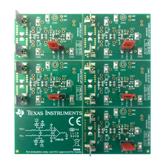
Page 4: Hardware
(EMC) testing. The INA191EVM consists of one PCB with an option to cut out five individual PCBs, one for each of the five gain options (A1 to A5) listed in Table 1. -
Page 5: Operation
Operation Quick Start Setup Follow these procedures to set up and use one of the panels of the INA191EVM. For the following instructions, x = 1, 2, 3, 4, or 5, depending on the selected gain option. Step 1. Choose the desired gain option panel. -
Page 6: Evm Components
EVM Components www.ti.com EVM Components This section summarizes the INA191EVM components. For the following components, x = 1, 2, 3, 4, or 5, depending on the selected gain option. R1x, R2x, R4x, R7x, R8x, C2x, C3x, C4x, C5x, C6x R1x, R2x, R7x,R8x, and R4x are factory-installed 0-Ω 0603 resistors. -
Page 7: U1X (Ina191)
U1x (INA191) U1x is the location for the INA191Ax test device. Five device boards are supplied with the INA191EVM board. Each board is populated with one of the available device gains. This option allows users to test the devices and determine the gain setting that is best for a given application. -
Page 8: Schematic, Pcb Layout, And Bill Of Materials
NOTE: Board layouts are not to scale. These figures are intended to show how the board is laid out; they are not intended to be used for manufacturing INA191EVM PCBs. Schematics Figure 1 through Figure 5 show the schematics for the INA191EVM PCB. INA191EVM SBOU218A – February 2019 – Revised April 2019 Submit Documentation Feedback Copyright © 2019, Texas Instruments Incorporated... -
Page 9: Ina191Evm Schematic: Gain A1 Panel
Schematic, PCB Layout, and Bill of Materials www.ti.com Figure 1. INA191EVM Schematic: Gain A1 Panel SBOU218A – February 2019 – Revised April 2019 INA191EVM Submit Documentation Feedback Copyright © 2019, Texas Instruments Incorporated... -
Page 10: Ina191Evm Schematic: Gain A2 Panel
Schematic, PCB Layout, and Bill of Materials www.ti.com Figure 2. INA191EVM Schematic: Gain A2 Panel INA191EVM SBOU218A – February 2019 – Revised April 2019 Submit Documentation Feedback Copyright © 2019, Texas Instruments Incorporated... -
Page 11: Ina191Evm Schematic: Gain A3 Panel
Schematic, PCB Layout, and Bill of Materials www.ti.com Figure 3. INA191EVM Schematic: Gain A3 Panel SBOU218A – February 2019 – Revised April 2019 INA191EVM Submit Documentation Feedback Copyright © 2019, Texas Instruments Incorporated... -
Page 12: Ina191Evm Schematic: Gain A4 Panel
Schematic, PCB Layout, and Bill of Materials www.ti.com Figure 4. INA191EVM Schematic: Gain A4 Panel INA191EVM SBOU218A – February 2019 – Revised April 2019 Submit Documentation Feedback Copyright © 2019, Texas Instruments Incorporated... -
Page 13: Ina191Evm Schematic: Gain A5 Panel
Schematic, PCB Layout, and Bill of Materials www.ti.com Figure 5. INA191EVM Schematic: Gain A5 Panel SBOU218A – February 2019 – Revised April 2019 INA191EVM Submit Documentation Feedback Copyright © 2019, Texas Instruments Incorporated... -
Page 14: Pcb Layout
Schematic, PCB Layout, and Bill of Materials www.ti.com PCB Layout Figure 6 through Figure 12 illustrate the PCB layout for the INA191EVM. Figure 6. INA191EVM Top Overlay Figure 7. INA191EVM Bottom Overlay Figure 8. INA191EVM Top Layer Figure 9. INA191EVM Bottom Layer INA191EVM SBOU218A –... -
Page 15: Ina191Evm Drill Drawing
Schematic, PCB Layout, and Bill of Materials www.ti.com Figure 10. INA191EVM Top Solder Figure 11. INA191EVM Bottom Solder Figure 12. INA191EVM Drill Drawing SBOU218A – February 2019 – Revised April 2019 INA191EVM Submit Documentation Feedback Copyright © 2019, Texas Instruments Incorporated... -
Page 16: Bill Of Materials
Schematic, PCB Layout, and Bill of Materials www.ti.com Bill of Materials Table 4 provides the parts list for the INA191EVM. Table 4. Bill of Materials Designator Value Description Package Reference Part Number Manufacturer B1, B2, B3, B4, B5, B6, B7, B8, Bumpon, Hemisphere, 0.25 X 0.075, Clear... - Page 17 S104, S105, S111, S112, S113, S114, S115, S121, S122, S123, S124, S125 TP21, TP22, TP23, TP24, TP25 Test Point, Compact, White, TH Keystone5007 5007 Keystone SBOU218A – February 2019 – Revised April 2019 INA191EVM Submit Documentation Feedback Copyright © 2019, Texas Instruments Incorporated...
- Page 18 Changed the description, part number, and manufacturer for designators R51, R52, R53, R54, R55, R61, R62, R63, R64, ..........................R65 in Table 4 ...................... • Added missing sockets to table 4 Revision History SBOU218A – February 2019 – Revised April 2019 Submit Documentation Feedback Copyright © 2019, Texas Instruments Incorporated...
- Page 19 TI products. TI’s provision of these resources does not expand or otherwise alter TI’s applicable warranties or warranty disclaimers for TI products. TI objects to and rejects any additional or different terms you may have proposed. IMPORTANT NOTICE Mailing Address: Texas Instruments, Post Office Box 655303, Dallas, Texas 75265 Copyright © 2022, Texas Instruments Incorporated...
Need help?
Do you have a question about the INA191EVM and is the answer not in the manual?
Questions and answers