Sony NV-U74 Service Manual
Hide thumbs
Also See for NV-U74:
- Instruction manual (54 pages) ,
- Important information manual (28 pages)
Table of Contents
Advertisement
Quick Links
SERVICE MANUAL
Ver. 1.0 2008.10
COMPONENT MODEL NAME
Main unit
Cradle
Car battery adapter
The map and POI data may contain copyrighted
material. Copyrighted data on a "Memory Stick
Duo" should be used within the limits of the
copyright law. Do not violate the previsions of the
copyright law.
Copyright © 2008 ZENRIN CO., LTD. All Rights
Reserved.
© 2007 NAVTEQ All Rights Reserved
• Microsoft, Windows and Windows Vista are
registered trademarks of Microsoft Corporation in
the United States and other countries.
• "Memory Stick",
, "Memory Stick Duo",
, "Memory Stick PRO Duo",
, "Memory Stick Micro"
("M2"), "MagicGate",
and
are trademarks of Sony
Corporation.
"MagicGate" is a generic name of a copyright
protection technology, developed by Sony
Corporation.
Sony Corporation
9-889-298-01
2008J05-1
Audio&Video Business Group
©
2008.10
Published by Sony Techno Create Corporation
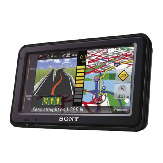
NV-U74
NV-U74
NVA-CU6
XA-DC3
Main unit
Operating temperature: 5 – 45 ºC (41 – 113 ºF)
Power requirements: DC 5 – 5.2 V
from supplied USB cable, optional AC adapter, or
supplied 12 V/24 V car battery adapter (negative
ground)
Connection terminals:
DC IN 5-5.2V jack
USB jack
External GPS antenna jack
Memory card slot: Memory Stick Duo slot
Speaker: ø30 mm (1.2 in) circular speaker
Consumption current: Max. 1.5 A
Dimensions: Approx. 133 × 79 × 20 mm
(5.2 × 3.1 × 0.8 in)
(w × h × d, protruding parts excluded)
, "nav-u"
Mass: Approx. 210 g (7.4 oz)
Monitor
System: Transmissive liquid crystal display
Dimensions: 4.3 in (16:9)
Approx. 95 × 54, 109 mm
(3.7 × 2.1, 4.3 in) (h × v, d)
Segment: 391,680 (816 × 480) dots
NV-U74
SPECIFICATIONS
Built-in battery charging time/usage
time
Charging time
With the supplied car battery adapter/optional AC
adapter: Approx. 2 hours (with unit turned on), or
1 hour (in standby mode)
With the supplied USB cable:
Approx. 2 hours (in standby mode)
Usage time
Up to 2 hours (depending on usage)
Supplied accessories
• Cradle
• Car battery adapter
• USB cable
• Quick Start Guide
• Important Information
• End-User License Agreement
• Warranty Card
Design and specifications are subject to change
without notice.
PERSONAL NAVIGATION SYSTEM
Mexican Model
Advertisement
Table of Contents

Related Manuals for Sony NV-U74


Summary of Contents for Sony NV-U74
- Page 1 (3.7 × 2.1, 4.3 in) (h × v, d) Segment: 391,680 (816 × 480) dots Design and specifications are subject to change without notice. PERSONAL NAVIGATION SYSTEM Sony Corporation 9-889-298-01 2008J05-1 Audio&Video Business Group © 2008.10 Published by Sony Techno Create Corporation...
-
Page 2: Table Of Contents
NV-U74 NOTES ON CHIP COMPONENT REPLACEMENT TABLE OF CONTENTS • Never reuse a disconnected chip component. • Notice that the minus side of a tantalum capacitor may be dam- SERVICING NOTES ..........aged by heat. GENERAL ..............FLEXIBLE CIRCUIT BOARD REPAIRING •... -
Page 3: Servicing Notes
NV-U74 SECTION 1 SERVICING NOTES UNLEADED SOLDER Boards requiring use of unleaded solder are printed with the lead- free mark (LF) indicating the solder contains no lead. (Caution: Some printed circuit boards may not come printed with the lead free mark due to their particular size) : LEAD FREE MARK Unleaded solder has the following characteristics. - Page 4 NV-U74 PRECAUTION WHEN CHECKING THE MAIN BOARD The MAIN board is attached with multiple shield plates. For electrical check or replacement of mounted parts, the shield plates must be removed and the frame of terminal board must be cut off.
-
Page 5: General
NV-U74 SECTION 2 This section is extracted GENERAL from instruction manual. Location of controls (on/standby) switch Display window/touch screen Nameplate Built-in GPS antenna MENU button Speaker GPS ANT (GPS antenna) jack VOICE/POS. button RELEASE button (USB) jack Shows the current position and Memory Stick access indicator DC IN 5-5.2V jack... - Page 6 NV-U74 Detaching the unit Detaching the cradle Press and hold RELEASE to release the unit. IMPORTANT Follow the instructions below to avoid damaging the surface of the suction cup. Turn the lever clockwise to unlock the cradle. Use the tab to detach the cradle Close the built-in GPS antenna.
-
Page 7: Disassembly
NV-U74 SECTION 3 DISASSEMBLY • This set can be disassembled in the order shown below. 3-1. DISASSEMBLY FLOW 3-2. CAP (Page 7) 3-3. FRONT BLOCK ASSY, REAR PANEL BLOCK ASSY (Page 8) – REAR PANEL – REAR PANEL BLOCK ASSY –... -
Page 8: Front Block Assy, Rear Panel Block Assy
NV-U74 3-3. FRONT BLOCK ASSY, REAR PANEL BLOCK ASSY rear panel block assy two screws (M1.7) two claws Open the rear panel block assy in the direction of the arrow. two screws (M1.7) LCD flexible board (CN5002) two claws TOUCH PANEL SWITCH flexible board... -
Page 9: Liquid Crystal Display Panel (Lcd5001), Touch Panel (Tps5001)
NV-U74 3-5. LIQUID CRYSTAL DISPLAY PANEL (LCD5001), TOUCH PANEL (TPS5001) bracket (right) two support plates two adhesive (support plates) liquid crystal display panel (LCD5001) cushion (D) Remove the liquid crystal display panel (LCD5001) in the direction of the arrow. (four claws) -
Page 10: Main Board
NV-U74 3-6. MAIN BOARD cushion (D) lower support cushion (LCD) connector (CN2501) MAIN board screw (P2) adhesive (PWB) connector with wire lead (CN0104, CN0105) sheet (GPS wire) speaker connector (CN3502) bottom side GPS antenna connector (CN0102) top side battery connector... -
Page 11: Test Mode
NV-U74 SECTION 4 TEST MODE 1. PREPARATION OF THE SERVICE MODE 4-2. Exception History Prepare the following before confi rming the service mode. • Memory Stick Duo (128 MB or more) 2. OUTLINE OF THE SERVICE MODE Necessary following function can be used by service by executing the service mode. - Page 12 NV-U74 6. NOTE OF CHECKING THE TEST MODE 10-1-3. Map ver Program data for test mode and special USB cable for test mode is This mode is not displayed in this set. (It is always displayed as necessary to confi rm the test mode.
- Page 13 NV-U74 2. moviNAND 10-3-2. HW Confi g When “moviNAND” on the screen is selected, and the “EXEC” When the “INFO” button is touched, the system will popup one button is touched, NAND fl ash memory (IC2001) is diagnosed. dialog to display information in detail.
- Page 14 NV-U74 5. White 0% 10-4-4. Touch panel When “White 0%” on the screen is selected, and the “EXEC” but- 1. Test ton is touched, black is displayed on full screen. To release from The “Test” button is touched, touch panel test screen is displayed.
- Page 15 NV-U74 10-5. Audio Test (Audio) 10-6-1. GPS Information 10-7. Cradle Test (Cradle) 10-9. Firmware Update (FWUpdate) The “GPS Information” button is touched, GPS information is dis- This mode is not used in servicing. played on screen usually. It is displayed at the error as “GPS port can’t open”...
-
Page 16: Diagrams
NV-U74 SECTION 5 DIAGRAMS 5-1. BLOCK DIAGRAM - GPS/MEMORY/LCD Section - NAND FLASH MEMORY IC2001 IC1001 (1/3) R0 – R7, G0 – G7, B0 – B7 MNAND_DAT0 – LDD0 – LDD4, DAT0 – DAT3 MNAND_DAT3 LDD6 – LDD15 HSYNC CLK M6... -
Page 17: Block Diagram - Main Section
NV-U74 5-2. BLOCK DIAGRAM - MAIN Section - AUDIO CODEC, TOUCH SCREEN CONTROLLER IC1001 (2/3) IC3501 CN4003 (USB) LINE AMP POWER AMP AC97_SDATA_OUT 5 SDATAOUT MONOOUT SP3501 SIGNAL IC3503 IC3504 A11 STD_TXD SELECTOR AC97_SDATA_IN_0 8 SDATAIN IC4503 AC97_BITCLK 6 BITCLK... -
Page 18: Block Diagram - Power Supply Section
NV-U74 5-3. BLOCK DIAGRAM - POWER SUPPLY Section - B+ SWITCH SYS3V Q3007, 3008 POWER CONTROL IC3002 FB3025 BU3V2 VINDCDC2 36 VDCDC2 B+ SWITCH LCD3.2V Q3009, 3010, IC1001 (3/3) 3013, 3014 LCF3.2V_ON SYS3.2V VINDCDC1 VDCDC1 DCDC1_EN 25 VINDCDC3 5 PWR_CORE... - Page 19 NV-U74 THIS NOTE IS COMMON FOR PRINTED WIRING BOARDS AND SCHEMATIC DIAGRAMS. • Waveforms (In addition to this, the necessary note is printed in each block.) – MAIN Board – For Printed Wiring Boards. For Schematic Diagrams. IC3501 (BITCLK) X1001...
-
Page 20: Printed Wiring Board - Main Board (Component Side)
NV-U74 5-4. PRINTED WIRING BOARD - MAIN Board (Component Side) - • : Uses unleaded solder. • Semiconductor MAIN BOARD (COMPONENT SIDE) Location Ref. No. Location D3002 S3004 D3003 R4004 D3005 D3006 R4029 D3010 ET002 D3014 D3016 D4007 D3020 D3021... -
Page 21: Printed Wiring Board - Main Board (Conductor Side)
NV-U74 5-5. PRINTED WIRING BOARD - MAIN Board (Conductor Side) - • : Uses unleaded solder. • Semiconductor MAIN BOARD (CONDUCTOR SIDE) Location Ref. No. Location D0101 F-12 JL3501 C3057 D3004 R1502 D3007 I-10 D3008 H-10 D3009 D3018 I-11 D3019... -
Page 22: Schematic Diagram - Main Board (1/10)
NV-U74 5-6. SCHEMATIC DIAGRAM - MAIN Board (1/10) - • See page 19 for Waveforms. • See page 37 for IC Pin Function Description. MAIN BOARD (1/10) R1127 LCD_HSYNC LCD_HSYNC_CPU LCD_B0 SP1_XMUTE LCD_B0 SP1_XMUTE MAIN LCD_B1 R1121 BOARD LCD_B1 LCD_VSYNC... -
Page 23: Schematic Diagram - Main Board (3/10)
NV-U74 5-7. SCHEMATIC DIAGRAM - MAIN Board (2/10) - • See page 33 for IC Block Diagrams. (2/10) MAIN BOARD SYS3V BU3V2 FB1501 MAIN C1507 BOARD (10/10) (Page 31) FL1502 MD31 MD31 MD30 MD30 MD29 MD29 MD28 MD28 MD27 (Chip Size Package) -
Page 24: Schematic Diagram - Main Board (6/10)
NV-U74 5-8. SCHEMATIC DIAGRAM - MAIN Board (3/10) - (3/10) MAIN BOARD R2013 JL4013 MNAND_CMD JL4014 R2012 MNAND_CLK JL4017 MNAND_DAT2 DAT0 RB2001 JL4016 MAIN MNAND_DAT1 DAT1 BOARD JL4015 (1/10) MNAND_DAT0 DAT2 JL4018 (Page 22) MNAND_DAT3 DAT3 JL4019 DAT4 RB2002 JL4020... - Page 25 NV-U74 5-9. SCHEMATIC DIAGRAM - MAIN Board (4/10) - MAIN BOARD (4/10) CN5002 FB5001 VDD_2.5V C5006 C5007 C5005 VD5005 VDD_2.5V 0.001 5V -->GND 5V -->GND LCD_R0 LCD_R0 LCD_R1 LCD_R1 R3069 LCD_R2 LCD_R0 470k LCD_R2 Q3010 LCD_R3 LCD_R1 JL3016 LCD_R3 RTR020P02TL...
-
Page 26: Schematic Diagram - Main Board (8/10)
NV-U74 5-10. SCHEMATIC DIAGRAM - MAIN Board (5/10) - • See page 19 for Waveforms. • See page 33 for IC Block Diagrams. • See page 37 for IC Pin Function Description. MAIN BOARD (5/10) R0207 MAIN GPS_1PPS BOARD (1/10) -
Page 27: Schematic Diagram - Main Board (9/10)
NV-U74 5-11. SCHEMATIC DIAGRAM - MAIN Board (6/10) - • See page 19 for Waveforms. • See page 33 for IC Block Diagrams. (6/10) MAIN BOARD R0208 JL0210 IC0203 BUFFER C0202 IC0203 TC7SZ126FU(TE85R) R0203 XGPS_RESET JL0211 (Page 22) R0201 MAIN... -
Page 28: Schematic Diagram - Main Board (10/10)
NV-U74 5-12. SCHEMATIC DIAGRAM - MAIN Board (7/10) - • See page 33 for IC Block Diagrams. • See page 37 for IC Pin Function Description. MAIN BOARD (7/10) RB4502 P1[6] P1[4] P0[0] XACC_IN_HUB R4527 P1[2] P0[2] USB_XCHGON 100k MAIN... - Page 29 NV-U74 5-13. SCHEMATIC DIAGRAM - MAIN Board (8/10) - • See page 19 for Waveforms. • See page 37 for IC Pin Function Description. (8/10) MAIN BOARD XRESET_OUT Q2501 LSK3019FP8TL MSLED_EN LED DRIVE C2504 C2506 R2506 4700 X2501 12MHz R2503...
- Page 30 NV-U74 5-14. SCHEMATIC DIAGRAM - MAIN Board (9/10) - • See page 33 for IC Block Diagrams. • See page 19 for Waveforms. • See page 37 for IC Pin Function Description. MAIN BOARD (9/10) IC3503 LINE AMP FB3504 IC3503...
- Page 31 NV-U74 5-15. SCHEMATIC DIAGRAM - MAIN Board (10/10) - • See page 33 for IC Block Diagrams. (10/10) MAIN BOARD F3001 2.5A C3002 D3016 LF3001 BATT_CHK JL3001 JL3004 JL3021 D1FM3 JL3014 J3001 MA+B DC IN MAIN 5-5.2V BOARD R3123 (9/10) R3075 SYS3.2V...
-
Page 32: 5-16. Printed Wiring Board - Ms Duo Board
NV-U74 5-16. PRINTED WIRING BOARD - MS DUO Board - 5-17. SCHEMATIC DIAGRAM - MS DUO Board - • : Uses unleaded solder. MS DUO BOARD (SIDE A) (Page 29) MS DUO BOARD MAIN BOARD (8/10) CN2501 CN9301 SYS5V SYS5V... - Page 33 NV-U74 • IC Block Diagrams – MAIN Board – IC0111 S-1167B15-M5T1G VIN 1 VOUT OVERCURRENT PROTECTION VSS 2 ON/OFF ON/OFF 3 CONTROL – REFERENCE VOLTAGE IC0112 S-1323B2JNB-N9QTFG IC0124 S-1323B30NB-N8PTFG VOUT 1 OVERCURRENT PROTECTION ON/OFF ON/OFF CONTROL – VSS 2 REFERENCE...
- Page 34 NV-U74 IC3002 TPS65020RHAR 30 SCLK SERIAL INTERFACE 29 SDAT THERMAL DC/DC SHUTDOWN STEP DOWN 28 INT CONVERTER 2 27 RESPWRON 26 TRESPWRON 25 DCDC1_EN CONTROL 24 DCDC2_EN DEFDCDC3 DC/DC 23 DCDC3_EN VDCDC3 STEP DOWN 22 LDO_EN PGND3 CONVERTER 3 VINDCDC3...
- Page 35 NV-U74 IC3003 LTC4055EUF#TR 16 15 ENABLE TIMER – 0.25V IN2 1 VOLTAGE CHARGER DETECT CC/CV REGULATOR UVLO BAT 2 HOLD OSCILLATOR RESET STOP COUNTER SOFT-START2 CURRENT LIMIT OUT 3 2.8V BATTERY BAT UV ICHRG UVLO – ILIM CNTL ENABLE 4.1V...
- Page 36 NV-U74 IC3005 TPS61027DRCR 10 PGND BACKGATE CONTROL OSCILLATOR VOUT CONTROL TEMPERATURE LOGIC CONTROL 9 SW 8 PS – REGULATOR ERROR – GATE VMAX CONTROL CONTROL – 7 LBI ANTI- 6 VBAT LOW BATTERY – RINGING COMPARATOR IC3504 TPA2010D1YZFR IC4501 S-T111B33MC-OGSTFG...
- Page 37 NV-U74 • IC Pin Function Description MAIN BOARD IC0105 GSC3ELP7975TR (GPS CONTROLLER) Pin No. Pin Name Description GND_BB Ground terminal GPIO1/ODO Not used RESERVED Not used GPIO0 Not used Serial data input from the CPU Serial data output to the CPU...
- Page 38 NV-U74 Pin No. Pin Name Description EA16, EA15, EA13, G5 to G9 Address signal output to the fl ash memory EA11, EA9 ON_OFF Soft on/off request signal input terminal Not used XSS1/GPIO4 SPI slave select signal input/output terminal Not used...
- Page 39 NV-U74 MAIN BOARD IC1001 RTPXA270C5C520 (CPU) Pin No. Pin Name Description A1, A2 VSS_CORE Ground terminal XCS1 Chip select signal output terminal Not used VCC_MEM Power supply terminal (+3V) VCC_SRAM Power supply terminal (+1.1V) Address signal output to the NOR fl ash memory VCC_CORE Power supply terminal (+1.5V)
- Page 40 NV-U74 Pin No. Pin Name Description GPS_1PPS Precise positioning service signal input from the GPS controller MNAND_DAT3 Two-way data bus with the NAND fl ash memory Cradle detaching/attaching detection signal input terminal “L”: cradle is attached XCRADLE_ON Fixed at “L” in this set...
- Page 41 NV-U74 Pin No. Pin Name Description LDD4 RGB (blue) signal output to the liquid crystal display LDD5 RGB signal output terminal Not used LDD3 RGB (blue) signal output to the liquid crystal display J1 to J3 MA3, MA6, MA7 Address signal output to the NOR fl ash memory...
- Page 42 NV-U74 Pin No. Pin Name Description VCC_CORE Power supply terminal (+1.5V) MD23 Two-way data bus with the SD-RAM VCC_CORE Power supply terminal (+1.5V) Two-way data bus with the SD-RAM and NOR fl ash memory VSS_MEM Ground terminal Mode select signal input terminal for JTAG...
- Page 43 NV-U74 Pin No. Pin Name Description AA17 GPIO97 Not used AA18 CIF_DD4 Input terminal for the setting AA19 VSS_IO Ground terminal AA20 PWR_CAP3 External capacitor connection terminal AA21 Ground terminal AA22 TXTAL_IN Sub system clock input terminal (32.768 kHz) AA23 TXTAL_OUT Sub system clock output terminal (32.768 kHz)
- Page 44 NV-U74 Pin No. Pin Name Description SDCLK2 Clock signal output terminal Not used VCC_CORE Power supply terminal (+1.5V) NOR_XWP Write protect signal output to the NOR fl ash memory SDCKE Clock enable signal output to the SD-RAM SDCLK1 Clock signal output to the SD-RAM...
- Page 45 NV-U74 MAIN BOARD IC2501 RTS5116-01H-GR (MEMORY STICK CONTROLLER) Pin No. Pin Name Description EECS Chip select signal output terminal for EEPROM Not used AGND Ground terminal System clock output terminal (12 MHz) System clock input terminal (12 MHz) A3V3 Power supply terminal (+3.2V)
- Page 46 NV-U74 MAIN BOARD IC3501 WM9705SEFL/RV (AUDIO CODEC, TOUCH SCREEN CONTROLLER) Pin No. Pin Name Description DVDD1 Power supply terminal (+3.2V) (digital system) XTLIN System clock input terminal (24.576 MHz) XTLOUT System clock output terminal (24.576 MHz) DGND1 Ground terminal (digital system)
- Page 47 NV-U74 MAIN BOARD IC4505 CY7C66113C-LFXC-CP6737AM (USB CONTROLLER) Pin No. Pin Name Description D- [0] Two-way USB data (-) bus with the USB connector P3 [3] Not used Ground terminal P3 [5] Not used D+ [1] Two-way USB client data (+) bus with the CPU...
-
Page 48: Exploded Views
(TPS5001). Refer to test mode “10-4-4. Touch panel” (page 14) for the calibration. Ref. No. Part No. Description Remark Ref. No. Part No. Description Remark 3-261-131-11 EMBLEM (NO.3), SONY 3-282-779-01 CUSHION (CHG) 3-212-726-11 INDICATOR (CHG) 2-650-652-11 CUSHION (D) 3-212-723-31 PANEL, FRONT 4-110-542-02 SUPPORT PLATE... -
Page 49: Rear Panel Block Assy Section
NV-U74 6-2. REAR PANEL BLOCK ASSY SECTION ANT001 not supplied BAT3001 MAIN board supplied supplied not supplied SP3501 not supplied Note 1: Ref. No. 72 cannot re-used. Note 2: When the MAIN board is exchanged, it is necessary to Please replace to brand-new part ones copper leaf sheet do some works. -
Page 50: Electrical Parts List
NV-U74 SECTION 7 MAIN ELECTRICAL PARTS LIST Note: • Due to standardization, replacements in • RESISTORS When indicating parts by reference num- the parts list may be different from the All resistors are in ohms. ber, please include the board name. - Page 51 NV-U74 MAIN Ref. No. Part No. Description Remark Ref. No. Part No. Description Remark C1512 1-125-777-11 CERAMIC CHIP 0.1uF C3049 1-125-777-11 CERAMIC CHIP 0.1uF C1514 1-125-777-11 CERAMIC CHIP 0.1uF C3057 1-164-943-81 CERAMIC CHIP 0.01uF C1515 1-125-777-11 CERAMIC CHIP 0.1uF C3058 1-107-826-11 CERAMIC CHIP 0.1uF...
- Page 52 NV-U74 MAIN Ref. No. Part No. Description Remark Ref. No. Part No. Description Remark C4503 1-125-777-11 CERAMIC CHIP 0.1uF FB1005 1-400-576-11 ARRAY, FERRITE CHIP C4504 1-125-777-11 CERAMIC CHIP 0.1uF FB1006 1-400-576-11 ARRAY, FERRITE CHIP C4505 1-164-943-81 CERAMIC CHIP 0.01uF C4506 1-164-943-81 CERAMIC CHIP 0.01uF...
- Page 53 NV-U74 MAIN Ref. No. Part No. Description Remark Ref. No. Part No. Description Remark IC3002 (Not supplied) IC TPS65020RHAR R0005 1-218-977-11 METAL CHIP 100K 1/16W IC3003 (Not supplied) IC LTC4055EUF#TR R0006 1-218-977-11 METAL CHIP 100K 1/16W IC3004 6-711-612-01 IC CAT4238TD-GT3...
- Page 54 NV-U74 MAIN Ref. No. Part No. Description Remark Ref. No. Part No. Description Remark R1048 1-218-937-11 METAL CHIP 1/16W R2003 1-218-975-11 METAL CHIP 1/16W R1049 1-218-937-11 METAL CHIP 1/16W R2004 1-218-975-11 METAL CHIP 1/16W R1052 1-218-977-11 METAL CHIP 100K 1/16W...
- Page 55 NV-U74 MAIN Ref. No. Part No. Description Remark Ref. No. Part No. Description Remark R3052 1-218-990-81 SHORT CHIP R3536 1-218-977-11 METAL CHIP 100K 1/16W R3054 1-216-837-11 METAL CHIP 1/10W R3538 1-218-990-81 SHORT CHIP R3056 1-216-864-11 SHORT CHIP R3539 1-218-990-81 SHORT CHIP...
- Page 56 NV-U74 MAIN MS DUO Ref. No. Part No. Description Remark Ref. No. Part No. Description Remark < VARISTOR > ACCESSORY ********** VD3001 1-805-043-11 ABSORBER, CHIP SURGE VD3502 1-805-043-11 ABSORBER, CHIP SURGE 4-114-985-11 MANUAL (QUICK START GUIDE) VD3503 1-805-043-11 ABSORBER, CHIP SURGE...
- Page 57 NV-U74 MEMO...
- Page 58 NV-U74 REVISION HISTORY Checking the version allows you to jump to the revised page. Also, clicking the version at the top of the revised page allows you to jump to the next revised page. Ver. Date Description of Revision 2008.10...
Need help?
Do you have a question about the NV-U74 and is the answer not in the manual?
Questions and answers