Advertisement
Quick Links
CP2130 E
VALUATION
1. Introduction
The CP2130 Evaluation Kit consists of a CP2130 Evaluation Board and software package to demonstrate the use
of the CP2130 USB-to-SPI bridge to communicate with several SPI slave devices, including an on-board SPI ADC
and SPI EEPROM. Several PC applications are included to demonstrate the CP2130 features and evaluate SPI
performance.
2. Kit Contents
The CP2130 Evaluation Kit contains the following items:
CP2130 Evaluation Board
Mini-USB Cable
CP21xx Installation DVD
Quick Start Guide
3. Relevant Documentation
Application notes can be found on the Interface Application Notes page for all fixed-function devices:
www.silabs.com/interface-appnotes.
AN721: CP21xx Device Customization Guide—Customize the VID, PID, serial number, and other
parameters stored in the CP2130 one-time programmable ROM.
AN792: CP2130 Interface Specification—Describes the USB control and bulk transfers for CP2130
devices as well as GPIO configuration.
4. Software Setup
The Software Development Kit (SDK) for the CP2130 Evaluation Kit is included on the kit DVD. The latest version
of this installer can also be downloaded from the
Documentation—data sheet, application notes, user's guide, quick start guide, and SLAB_USB_SPI
interface library API documentation.
CP2130 Demo—Example software utilizing the SLAB_USB_SPI interface library API to demonstrate the
CP2130 Evaluation Board features.
CP2130 Evaluation Tool—Advanced evaluation software used to execute low-level SPI transfers, control
GPIO outputs, and retrieve device information.
AN721 Device Customization Utility—Customization software used to program the one-time
programmable ROM.
Library—SLAB_USB_SPI interface library and header files used to interface between a user application
and USB driver such as Microsoft's WinUSB driver.
The Windows installer should launch automatically after inserting the
SDK to the system.
Rev. 0.2 10/13
K
U
IT
SER
www.silabs.com/cp2130ek
Copyright © 2013 by Silicon Laboratories
C P 2 1 3 0 - E K
'
G
S
UIDE
web site. This package includes:
. Follow the instructions to install the
DVD
CP2130-EK
Advertisement

Related Manuals for Silicon Laboratories CP2130


Summary of Contents for Silicon Laboratories CP2130
- Page 1 AN792: CP2130 Interface Specification—Describes the USB control and bulk transfers for CP2130 devices as well as GPIO configuration. 4. Software Setup The Software Development Kit (SDK) for the CP2130 Evaluation Kit is included on the kit DVD. The latest version of this installer can also be downloaded from the www.silabs.com/cp2130ek web site.
- Page 2 1. Connect the CP2130 Evaluation Board to a PC as shown in Figure 1. 2. Connect one end of the mini-USB cable to a USB Port on the PC. 3. Connect the other end of the mini-USB cable to the mini-USB connector on the CP2130 Evaluation Board. Mini-USB Cable Figure 1.
- Page 3 Microsoft Driver Package Installer (DPInst) to install the Microsoft WinUSB driver. The SDK installer will automatically install the driver on Windows machines. The CP2130 appears as a “Silicon Labs CP2130 USB to SPI Bridge” in Device Manager as shown in Figure 2. Figure 2. CP2130 in Device Manager 7.
- Page 4 1. Make sure that the hardware is connected to a Windows PC as shown in Figure 1. If the device is properly connected, the green Active LED on the CP2130 Evaluation Board will turn on. After a few seconds of inactivity, the green Active LED may turn off, and the red Suspend LED will then turn on to indicate that the device has entered USB suspend mode.
- Page 5 CP2130-EK 5. Connect to the CP2130 USB-to-SPI bridge by selecting the device in the Device Selection combo box and clicking the Connect button. Figure 4. Connecting to a CP2130 Evaluation Board Rev. 0.2...
- Page 6 CP2130-EK 6. Observe the potentiometer voltage displayed in the Potentiometer Voltage gauge. Rotate the potentiometer and watch the voltage change. 7. Observe the temperature sensor value displayed in the Temperature Sensor gauge. Figure 5. Reading the Potentiometer and Temperature Sensor ADC Channel Inputs...
- Page 7 CP2130-EK 8. Run SPI throughput tests using CS1: a. Select the transfer mode from the combo box. The following SPI transfer modes are available: Write, Read, Write/Read (simultaneous write and read). b. Click the Run Speed Test button to run a short throughput test using the selected transfer mode or click the Continuous checkbox and then click Run Speed Test to run a continuous throughput test.
- Page 8 CP2130-EK 9. Configure the general purpose input/output (GPIO) pins and read and write the pin latch values: a. Select the GPIO pin mode from the Pin Config combo box. The following pin modes are available: Input, Open Drain, or Push-Pull. When a GPIO pin is configured in Input mode, the latch value can only be read and not written.
- Page 9 CP2130-EK 10. Write and read back a string to the external SPI EEPROM: a. Enter a string into the Write text box. Click the Write button to write the string to the external EEPROM. b. Click the Read button to read the string from the external EEPROM and display the string in the Read text box.
- Page 10 CP2130-EK 11. Use the CP2130 event counter feature to monitor push-button presses on the EVENT button which is connected to GPIO.4 / CS4 / EVTCNTR: a. Press the EVENT button on the CP2130 Evaluation Board. Notice that the Event Counter Counts field updates to reflect the total number of button presses.
- Page 11 CP2130-EK 12. Plot the ADC analog input sample values: a. Click the Plot ADC button to open the plot window. b. Select one of the three ADC channels to plot. The following ADC channels are available: Potentiometer (CH.0), Temp Sensor (CH.1), or (CH.2). By default, Channel 2 is connected to GPIO.5 / CS5 / CLKOUT.
- Page 12 1. Make sure that the hardware is connected to a Windows PC as shown in Figure 1. If the device is properly connected, the green Active LED on the CP2130 Evaluation Board will turn on. After a few seconds of inactivity, the green Active LED may turn off, and the red Suspend LED will then turn on to indicate that the device has entered USB suspend mode.
- Page 13 CLKOUT mode, this divider is used to control the output frequency. The CLKOUT divider reset value is stored in the one-time programmable ROM but may be changed at runtime. j. Computed CLKOUT Frequency—The CLKOUT frequency calculated from the CP2130 system clock divided by the CLKOUT divider.
- Page 14 Toggle CS—Specifies that the chip-select pin will be toggled after each SPI byte transferred. vii. Post-Assert Delay—Specifies the amount of time that the CP2130 will delay after the last SPI byte has been transferred before deasserting the chip-select pin. The delay is in units of 10 µs.
- Page 15 CP2130-EK Figure 13. Configuring an SPI Transfer Rev. 0.2...
- Page 16 CP2130-EK 7. To execute a WriteRead SPI transfer: a. Select the WriteRead radio button from the SPI Transfer Type group box. b. Configure the Test Configuration and SPI Parameters, making sure to enter the number of bytes to read/write in the Total Bytes (<1M) text field.
- Page 17 CP2130-EK 8. To execute an asynchronous Read SPI transfer: a. Select the Read (Asynchronous) radio button from the SPI Transfer Type group box. b. Enter the maximum number of bytes to read in the Total Bytes (<1M) text field. Enter a maximum timeout, which specifies the maximum amount of time the read transfer can take in milliseconds.
- Page 18 CP2130-EK 9. Click the Reset button to send the Reset command to the CP2130. After the device receives this command, it will perform a reset and re-enumerate on the bus. 10. GPIO pins configured as GPIO outputs can controlled using the GPIO Toggle buttons. Click the GPIO pin 0–10 button to toggle the output latch value.
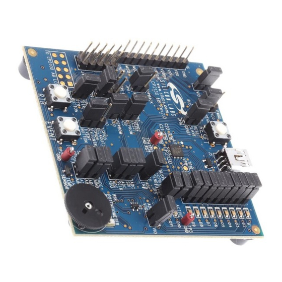
- Page 19 The CP2130 Evaluation Kit includes an evaluation board with a CP2130 pre-installed for evaluation and preliminary software development. The evaluation board also contains two SPI slave devices: an Si8902 Isolated Monitoring ADC and a 256 x 8 SPI EEPROM. Figure 17 and Figure 18 highlight the CP2130 Evaluation Board features.
- Page 20 CP2130-EK EEPROM Figure 18. CP2130 Evaluation Board Features (Back) Rev. 0.2...
- Page 21 MISO MISO JP13 JP11 EEPROM JP21 EEPROM MOSI JP19 JP12 CLKOUT MISO EVTCNTR JP10 BUTTON BUTTON AIN0 JP18 JP17 AIN1 TEMP TO CP2400 AB LCD AIN2 CLKOUT EVENT Figure 19. CP2130 Evaluation Board with Default Shorting Blocks Installed Rev. 0.2...
- Page 22 CP2130-EK 10.2. CP2400 AB LCD Header (J3) This header can be used to connect the CP2130 to a CP2400 AB LCD expansion board. 10.3. SPI Monitor Header (J4) The SPI monitor terminal block is included to easily interace with a SPI monitoring device with a common 10-pin ribbon cable interface.
- Page 23 VDD voltage specification! USB bus-powered mode (Short Pins 2–3 on JP1)—VREGIN is shorted to VBUS and the CP2130 internal voltage regulator is enabled. The board VDD is powered by the CP2130 internal voltage regulator output.
- Page 24 10.7. LED Headers (JP3, JP4, and JP5) Headers JP3, JP4, and JP5 are provided to allow access to the GPIO pins on the CP2130. Place shorting blocks on JP3, JP4, and JP5 to connect the GPIO pins to the ten green LEDs, D1–D10, and the one red LED, D11. These LEDs can be used to indicate active communications through the CP2130.
- Page 25 This header provides access to the EEPROM chip-select pin. Install a shorting block on JP13 to connect the CP2130 CS2 pin to the EEPROM chip-select pin. See Table 11 for the EEPROM chip select header pin definitions. Table 11. EEPROM Chip-Select Header Pin Definitions...
- Page 26 10.14. ADC RST Header (JP16) This header provides access to the ADC reset pin. Install a shorting block on JP16 to allow the CP2130 to control the ADC reset pin via GPIO.7. See Table 12 for the ADC reset header pin definitions.
- Page 27 MISO JP21[5:6] 10.19. VIO Header (JP22) This header provides access to the CP2130 VIO pin. Install a shorting block on JP22 short VIO to VDD. See Table 17 for the VIO header pin definitions. Table 17. VIO Header Pin Definitions...
- Page 28 CP2130-EK 11. Schematics Rev. 0.2...
- Page 29 CP2130-EK Rev. 0.2...
- Page 30 CP2130-EK 12. Bill of Materials Table 18. CP2130 Evaluation Board Bill of Materials Reference Part Number Source Description C1, C5, C7, C0603X5R160-105K Venkel 1 µF 16 V ±10% X5R C0603 C9, C20, C22, C24, C30 C2, C4, C6, C0402X7R160-104K Venkel 0.1 µF 16 V ±10% X7R C0402...
- Page 31 CP2130-EK Table 18. CP2130 Evaluation Board Bill of Materials (Continued) Reference Part Number Source Description TSW-110-07-T-S Samtec HEADER 0.1in-1x10 Header CONN1X10 NTR4171PT1G ON Semiconductor NTR4171PT1G -30V P-CHNL SOT23- 470 ±5% ThickFilm R0402 R1, R2, R3, CR0402-16W-471J Venkel R4, R5, R6,...
-
Page 32: Contact Information
Silicon Laboratories products are not designed, intended, or authorized for use in applications intend- ed to support or sustain life, or for any other application in which the failure of the Silicon Laboratories product could create a situation where personal injury or death may occur. - Page 33 Компания «ЭлектроПласт» предлагает заключение долгосрочных отношений при поставках импортных электронных компонентов на взаимовыгодных условиях! Наши преимущества: Оперативные поставки широкого спектра электронных компонентов отечественного и импортного производства напрямую от производителей и с крупнейших мировых складов; Поставка более 17-ти миллионов наименований электронных компонентов; ...
Need help?
Do you have a question about the CP2130 and is the answer not in the manual?
Questions and answers