Table of Contents
Advertisement
Quick Links
Advertisement
Table of Contents

Related Manuals for Seco COM-Express CCOMe-C96


Summary of Contents for Seco COM-Express CCOMe-C96
- Page 1 CCOMe-C96 Carrier Board for COM-Express Type 6 Module on ATX form factor...
- Page 2 SECO S.p.A. reserves the right to change precise specifications without prior notice to supply the best product possible. For further information on this module or other SECO products, but also to get the required assistance for any and possible issues, please contact us using the dedicated web form available at https://www.seco.com/...
-
Page 3: Table Of Contents
PEG (PCI Express Graphics x16) Connector .................................. 39 eSPI/LPC Debug Connector ......................................43 COM ports and RS232 ports Internal pin Headers ................................44 CCOMe-C96 CCOMe-C96 - Rev. First Edition: 1.0 - Last Edition: 1.0 - Author: A.R. - Reviewed by C.M. Copyright © 2021 SECO S.p.A. - Page 4 JTAG Connector.......................................... 64 FAN Connector ........................................... 64 Buttons ............................................65 Appendices ....................................66 Thermal Design ........................................... 67 Accessories ............................................68 CCOMe-C96 CCOMe-C96 - Rev. First Edition: 1.0 - Last Edition: 1.0 - Author: A.R. - Reviewed by C.M. Copyright © 2021 SECO S.p.A.
-
Page 5: Introduction
Safety • Electrostatic Discharges • RoHS compliance • Safety Policy • Terminology and definitions • Reference specifications CCOMe-C96 CCOMe-C96 - Rev. First Edition: 1.0 - Last Edition: 1.0 - Author: A.R. - Reviewed by C.M. Copyright © 2021 SECO S.p.A. -
Page 6: Warranty
All changes or modifications to the equipment not explicitly approved by SECO S.p.A. could impair the equipment s functionality and could void the warranty. CCOMe-C96 CCOMe-C96 - Rev. First Edition: 1.0 - Last Edition: 1.0 - Author: A.R. - Reviewed by C.M. Copyright © 2021 SECO S.p.A. -
Page 7: Information And Assistance
SECO Sales Representative: the Sales Rep can help to determine the exact cause of the problem and search for the best solution. • SECO Help-Desk: contact SECO Technical Assistance. A technician is at disposal to understand the exact origin of the problem and suggest the correct solution. -
Page 8: Safety
The CCOMe-C96 board is designed using RoHS compliant components and is manufactured on a lead-free production line. It is therefore fully RoHS compliant. CCOMe-C96 CCOMe-C96 - Rev. First Edition: 1.0 - Last Edition: 1.0 - Author: A.R. - Reviewed by C.M. Copyright © 2021 SECO S.p.A. -
Page 9: Safety Policy
ES1 requirements; the board in its enclosure must be evaluated for temperature and airflow considerations. CCOMe-C96 CCOMe-C96 - Rev. First Edition: 1.0 - Last Edition: 1.0 - Author: A.R. - Reviewed by C.M. Copyright © 2021 SECO S.p.A. -
Page 10: Terminology And Definitions
Secure Digital Input/Output, an evolution of the SD standard that allows use the use of the same SD interface to drive different Input/Output CCOMe-C96 CCOMe-C96 - Rev. First Edition: 1.0 - Last Edition: 1.0 - Author: A.R. - Reviewed by C.M. Copyright © 2021 SECO S.p.A. - Page 11 Transistor-transistor Logic User Identity Module, an extension of SIM modules. Universal Serial Bus V_REF Voltage reference Pin CCOMe-C96 CCOMe-C96 - Rev. First Edition: 1.0 - Last Edition: 1.0 - Author: A.R. - Reviewed by C.M. Copyright © 2021 SECO S.p.A.
-
Page 12: Reference Specifications
SD Card Association https://www.sdcard.org SM Bus http://www.smbus.org/specs TMDS http://www.latticesemi.com/view_document?document_id=38351 USB 2.0 and USB OTG http://www.usb.org/developers/docs/usb20_docs/usb_20_080117.zip USB 3.0 http://www.usb.org/developers/docs/usb_31_080117.zip CCOMe-C96 CCOMe-C96 - Rev. First Edition: 1.0 - Last Edition: 1.0 - Author: A.R. - Reviewed by C.M. Copyright © 2021 SECO S.p.A. -
Page 13: Overview
• Introduction • Technical Specifications • Electrical Specifications • Mechanical Specifications • Block Diagram CCOMe-C96 CCOMe-C96 - Rev. First Edition: 1.0 - Last Edition: 1.0 - Author: A.R. - Reviewed by C.M. Copyright © 2021 SECO S.p.A. -
Page 14: Introduction
The robust thermal and mechanical concept, combined with extended power-management capabilities, is perfectly suited for all applications. CCOMe-C96 CCOMe-C96 - Rev. First Edition: 1.0 - Last Edition: 1.0 - Author: A.R. - Reviewed by C.M. Copyright © 2021 SECO S.p.A. -
Page 15: Technical Specifications
2.2 Technical Specifications Other Interfaces Supported Modules 4 x GPI + 4 x GPO pin header (interface multiplexed with µSD slot) COM Express Type 6 compliant modules SPI Flash header Mass Storage interfaces Button / LEDs front panel header 4x SATA 7p M connectors 4-pin tachometric FAN connector µSD Card slot (interface multiplexed with GPIO header) I2C + SM Bus on feature Pin header... -
Page 16: Electrical Specifications
+12V_RUN Mating Connector, MOLEX p/n 39-01-2060 or equivalent, with female crimp terminal MOLEX series 5566. +12V_RUN +12V_RUN CCOMe-C96 CCOMe-C96 - Rev. First Edition: 1.0 - Last Edition: 1.0 - Author: A.R. - Reviewed by C.M. Copyright © 2021 SECO S.p.A. - Page 17 Another diode LED D16, complementary to D17, is used to notify the Reset Output from Module to Carrier Board, directly driven through an High-Speed Buffer by CB_RESET# signal. CCOMe-C96 CCOMe-C96 - Rev. First Edition: 1.0 - Last Edition: 1.0 - Author: A.R. - Reviewed by C.M. Copyright © 2021 SECO S.p.A.
-
Page 18: Smart Battery Sm Bus Connector
RTC battery can be enabled/disabled using dedicated jumper on CN6, which is a standard pin header, P2.54mm, 1x3 pin. CCOMe-C96 CCOMe-C96 - Rev. First Edition: 1.0 - Last Edition: 1.0 - Author: A.R. - Reviewed by C.M. Copyright © 2021 SECO S.p.A. -
Page 19: Power Rails Meanings
_ALW: Always-on voltages, i.e. power rails that are active both in ACPI s S0 (Working), S3 (Standby) and S5 (Soft Off) state. Examples: +5V_ALW, +3.3V_ALW. CCOMe-C96 CCOMe-C96 - Rev. First Edition: 1.0 - Last Edition: 1.0 - Author: A.R. - Reviewed by C.M. Copyright © 2021 SECO S.p.A. -
Page 20: Mechanical Specifications
In order to fix the COM Express module to the carrier board, on CCOMe-C96 have been soldered six metallic spacers, height 8mm, 2.5mm diameter. CCOMe-C96 CCOMe-C96 - Rev. First Edition: 1.0 - Last Edition: 1.0 - Author: A.R. - Reviewed by C.M. Copyright © 2021 SECO S.p.A. -
Page 21: Block Diagram
2.5 Block Diagram RJ-45 Gigabit eSPI / LPC FuSa RSVD PEG X16 PCI-e x16 Slot Ethernet Connector Header Header SATA #[0..3] eSPI 4x SATA 7p Gen3 DDI1 Bridge eSPI-to-LPC DP connector #1 Connectors DDI2 DP connector #2 Port 80 4x 7-Segment DDI3 µSD Slot DP Connector #3... -
Page 22: Connectors
• Connectors placement • Connectors overview • Connectors description CCOMe-C96 CCOMe-C96 - Rev. First Edition: 1.0 - Last Edition: 1.0 - Author: A.R. - Reviewed by C.M. Copyright © 2021 SECO S.p.A. -
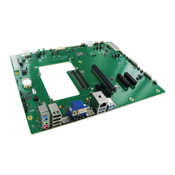
Page 23: Connectors Placement
3.1 Connectors placement On CCOMe-C96 carrier board, there are several connectors. Some of them are standard connectors, like Display Port, Gigabit Ethernet, USB ports, and are placed on the same side of the board, so that they can be placed on a panel of a possible enclosure. In the following picture it is possible to see the position of each connector. - Page 24 5V Current LCD PWR RTC battery mode sel mode sel selector selector selector selector Monitor sel enable CCOMe-C96 CCOMe-C96 - Rev. First Edition: 1.0 - Last Edition: 1.0 - Author: A.R. - Reviewed by C.M. Copyright © 2021 SECO S.p.A.
-
Page 25: Connectors Overview
SATA M 7-p #0 Connector CN25 SATA M 7-p #1 Connector CN26 RS-232 ports Internal pin Header CN27 Feature pin Header CCOMe-C96 CCOMe-C96 - Rev. First Edition: 1.0 - Last Edition: 1.0 - Author: A.R. - Reviewed by C.M. Copyright © 2021 SECO S.p.A. -
Page 26: Jumpers And Switch List
GPIO/SD Card selector JP11 eDP/LVDS selector JP12 Backlight Power selector JP13 LCD Power selector JP14 MIC1 / MIC2 selector CCOMe-C96 CCOMe-C96 - Rev. First Edition: 1.0 - Last Edition: 1.0 - Author: A.R. - Reviewed by C.M. Copyright © 2021 SECO S.p.A. -
Page 27: Connectors Description
GbEthernet Reference Voltage GBE0_CTREF SMB_DAT SM Bus Data Suspend to RAM (S3) signal SUS_S3# SMB_ALERT# SM Bus Alert signal CCOMe-C96 CCOMe-C96 - Rev. First Edition: 1.0 - Last Edition: 1.0 - Author: A.R. - Reviewed by C.M. Copyright © 2021 SECO S.p.A. - Page 28 USB3+ USB Data Port 3+ USB Over Current Ports 2/3 USB_2_3_OC# USB_0_1_OC# USB Over Current Ports 0/1 CCOMe-C96 CCOMe-C96 - Rev. First Edition: 1.0 - Last Edition: 1.0 - Author: A.R. - Reviewed by C.M. Copyright © 2021 SECO S.p.A.
- Page 29 LVDS Ch. A Data 1- / eDP Ch. Data 1- LVDS_A1-/eDP_TX1- LVDS_B1- LVDS Ch. B Data 1 - CCOMe-C96 CCOMe-C96 - Rev. First Edition: 1.0 - Last Edition: 1.0 - Author: A.R. - Reviewed by C.M. Copyright © 2021 SECO S.p.A.
- Page 30 B103 SLEEP# Sleep Button Input +12V switched power supply +12V_S A104 B104 +12V_S +12V switched power supply CCOMe-C96 CCOMe-C96 - Rev. First Edition: 1.0 - Last Edition: 1.0 - Author: A.R. - Reviewed by C.M. Copyright © 2021 SECO S.p.A.
- Page 31 PCI Express Transmit Pair 6- Power Ground Power Ground PCI Express Receive Pair 7+ PCIE_RX7+ PCIE_TX7+ PCI Express Transmit Pair 7+ CCOMe-C96 CCOMe-C96 - Rev. First Edition: 1.0 - Last Edition: 1.0 - Author: A.R. - Reviewed by C.M. Copyright © 2021 SECO S.p.A.
- Page 32 Digital Display interface 2 pair 3- Power Ground Power Ground PCIe Graphics receive pair 0+ PEG_RX0+ PEG_TX0+ PCIe Graphics transmit pair 0+ CCOMe-C96 CCOMe-C96 - Rev. First Edition: 1.0 - Last Edition: 1.0 - Author: A.R. - Reviewed by C.M. Copyright © 2021 SECO S.p.A.
- Page 33 PCIe Graphics transmit pair 9+ PCIe Graphics receive pair 9- PEG_RX9- PEG_TX9- PCIe Graphics transmit pair 9- CCOMe-C96 CCOMe-C96 - Rev. First Edition: 1.0 - Last Edition: 1.0 - Author: A.R. - Reviewed by C.M. Copyright © 2021 SECO S.p.A.
- Page 34 +12V switched power supply +12V_S C109 D109 +12V_S +12V switched power supply Power Ground C110 D110 Power Ground CCOMe-C96 CCOMe-C96 - Rev. First Edition: 1.0 - Last Edition: 1.0 - Author: A.R. - Reviewed by C.M. Copyright © 2021 SECO S.p.A.
-
Page 35: Pci-E X4 Slots
WAKE0# PCIEx4_1_RST# buffer. Active low signal, +3.3V_ALW electrical level with a 100k Not Connected RSVD Power Ground CCOMe-C96 CCOMe-C96 - Rev. First Edition: 1.0 - Last Edition: 1.0 - Author: A.R. - Reviewed by C.M. Copyright © 2021 SECO S.p.A. - Page 36 +12V_RUN PRSNT1# Hot Plug presence detect (tied to GND) +12V Power Rail +12V_RUN +12V_RUN +12V Power Rail CCOMe-C96 CCOMe-C96 - Rev. First Edition: 1.0 - Last Edition: 1.0 - Author: A.R. - Reviewed by C.M. Copyright © 2021 SECO S.p.A.
- Page 37 PCI-e Receiver lane 5+ Power Ground PCIE_RX5- PCI-e Receiver lane 5- PCI-e Transmitter lane 6+ PCIE_TX6+ Power Ground CCOMe-C96 CCOMe-C96 - Rev. First Edition: 1.0 - Last Edition: 1.0 - Author: A.R. - Reviewed by C.M. Copyright © 2021 SECO S.p.A.
- Page 38 In case that these pins are not tied together on the add-in card, then the carrier board will not acknowledge the presence of the card in the slot, and will not enable the reference clock (and the add-in card will not work). CCOMe-C96 CCOMe-C96 - Rev. First Edition: 1.0 - Last Edition: 1.0 - Author: A.R. - Reviewed by C.M. Copyright © 2021 SECO S.p.A.
-
Page 39: Peg (Pci Express Graphics X16) Connector
Power Ground PCI-e reference clock lane +, derived by Power Ground PEG_CLK+ PCIE_CK_REF+ using a Clock Buffer CCOMe-C96 CCOMe-C96 - Rev. First Edition: 1.0 - Last Edition: 1.0 - Author: A.R. - Reviewed by C.M. Copyright © 2021 SECO S.p.A. - Page 40 PCI-e Graphics Receiver lane 4- PCI-e Graphics Transmitter lane 5+ PEG_TX5+ Power Ground PCI-e Graphics Transmitter lane 5- PEG_TX5- Power Ground CCOMe-C96 CCOMe-C96 - Rev. First Edition: 1.0 - Last Edition: 1.0 - Author: A.R. - Reviewed by C.M. Copyright © 2021 SECO S.p.A.
- Page 41 PCI-e Graphics Receiver lane 11+ Power Ground PEG_RX11- PCI-e Graphics Receiver lane 11- PCI-e Graphics Transmitter lane 12+ PEG_TX12+ Power Ground CCOMe-C96 CCOMe-C96 - Rev. First Edition: 1.0 - Last Edition: 1.0 - Author: A.R. - Reviewed by C.M. Copyright © 2021 SECO S.p.A.
- Page 42 In case that these pins are not tied together on the add-in card, then the carrier board will not acknowledge the presence of the card in the slot, and will not enable the reference clock (and the add-in card will not work). CCOMe-C96 CCOMe-C96 - Rev. First Edition: 1.0 - Last Edition: 1.0 - Author: A.R. - Reviewed by C.M. Copyright © 2021 SECO S.p.A.
-
Page 43: Espi/Lpc Debug Connector
ESPI_RESET#: eSPI Reset Signal for both master and slaves devices ESPI_ALERT0#: eSPI signal used by eSPI slave to request service from the eSPI master CCOMe-C96 CCOMe-C96 - Rev. First Edition: 1.0 - Last Edition: 1.0 - Author: A.R. - Reviewed by C.M. Copyright © 2021 SECO S.p.A. -
Page 44: Com Ports And Rs232 Ports Internal Pin Headers
(a dual row p.254mm 9-pin header) is as described in the left table. COM1_CTS# COM1_Rx- COM2_CTS# COM2_Rx- CCOMe-C96 CCOMe-C96 - Rev. First Edition: 1.0 - Last Edition: 1.0 - Author: A.R. - Reviewed by C.M. Copyright © 2021 SECO S.p.A. - Page 45 9-pin standard male pin header, p 2.54 mm, 5+4 pin, h= 6mm, type NELTRON p/n 2213S-10G-E06 or equivalent. UART0_232_TX UART1_232_TX N.C. N.C. N.C. N.C. CCOMe-C96 CCOMe-C96 - Rev. First Edition: 1.0 - Last Edition: 1.0 - Author: A.R. - Reviewed by C.M. Copyright © 2021 SECO S.p.A.
- Page 46 For ESD protection, on all data and voltage lines are placed clamping diodes for voltage transient suppression. and +5V are derived from +5V_ALW through a 1A current limited power switch. USB0 USB1 CCOMe-C96 CCOMe-C96 - Rev. First Edition: 1.0 - Last Edition: 1.0 - Author: A.R. - Reviewed by C.M. Copyright © 2021 SECO S.p.A.
- Page 47 For ESD protection, on all data and voltage lines are placed clamping diodes for voltage transient suppression. and +5V are derived from +5V_ALW through a 1A current limited power switch. USB2 USB3 CCOMe-C96 CCOMe-C96 - Rev. First Edition: 1.0 - Last Edition: 1.0 - Author: A.R. - Reviewed by C.M. Copyright © 2021 SECO S.p.A.
- Page 48 USB_7+ Signal description: USB_4+/USB_4-: USB 2.0 Port #4 differential pair USB_5+/USB_5-: USB 2.0 Port #5 differential pair CCOMe-C96 CCOMe-C96 - Rev. First Edition: 1.0 - Last Edition: 1.0 - Author: A.R. - Reviewed by C.M. Copyright © 2021 SECO S.p.A.
- Page 49 USB_6_7_OC#: USB over-current sense signal for USB channels #6 and #7. Active Low Input Signal, electrical level +3.3V_ALW, manged by COM Express module. CCOMe-C96 CCOMe-C96 - Rev. First Edition: 1.0 - Last Edition: 1.0 - Author: A.R. - Reviewed by C.M. Copyright © 2021 SECO S.p.A.
- Page 50 SATA2_RX+/SATA2_RX-: Serial ATA Channel #2 Receive differential pair. SATA3_TX+/SATA3_TX-: Serial ATA Channel #3 Transmit differential pair. SATA3_RX+/SATA3_RX-: Serial ATA Channel #3 Receive differential pair. CCOMe-C96 CCOMe-C96 - Rev. First Edition: 1.0 - Last Edition: 1.0 - Author: A.R. - Reviewed by C.M. Copyright © 2021 SECO S.p.A.
- Page 51 COM Express module, it is biased using a Ultra High Speed CMOS buffer. Active Low Output Signal, +3.3V_ALW system is in Suspend to Disk (S4) state CCOMe-C96 CCOMe-C96 - Rev. First Edition: 1.0 - Last Edition: 1.0 - Author: A.R. - Reviewed by C.M. Copyright © 2021 SECO S.p.A.
- Page 52 SPI_HOLD#: this signal too is tied, through a 10kΩ resistor, to SPI_POWER signal. This means that when the Flash is powered, the Hold condition of serial communication is automatically removed. CCOMe-C96 CCOMe-C96 - Rev. First Edition: 1.0 - Last Edition: 1.0 - Author: A.R. - Reviewed by C.M. Copyright © 2021 SECO S.p.A.
- Page 53 All of these signals are derived directly from COM Express module’s VGA_xxxx corresponding signals, by placing ESD protections, EMI filters and voltage level shifters for DDC lines. CCOMe-C96 CCOMe-C96 - Rev. First Edition: 1.0 - Last Edition: 1.0 - Author: A.R. - Reviewed by C.M. Copyright © 2021 SECO S.p.A.
- Page 54 RSVD#D45 FUSA_SPIM_SCLK FUSA_I2C_DAT RSVD#C48 FUSA_SPIM_MISO FUSA_DIAGTEST_MODE RSVD#D48 FUSA_SPIM_MOSI FUSA_DIAGTEST_EN RSVD#C63 FUSA_PROCHOT FUSA_PROCHOT# RSVD#C64 FUSA_THERMTRIP FUSA_THERMTRIP# RSVD#D63 FUSA_CATERR# CCOMe-C96 CCOMe-C96 - Rev. First Edition: 1.0 - Last Edition: 1.0 - Author: A.R. - Reviewed by C.M. Copyright © 2021 SECO S.p.A.
- Page 55 RSVD#D64 FUSA_PCHHOT# RSVD#C77 FUSA_POWERFAIL# FUSA_POWERFAIL# SYS_RESET# PS_ON# PWR_BTN# CCOMe-C96 CCOMe-C96 - Rev. First Edition: 1.0 - Last Edition: 1.0 - Author: A.R. - Reviewed by C.M. Copyright © 2021 SECO S.p.A.
- Page 56 SDIO_DAT[0÷3]: SD Card data bus. SDIO_DAT0 signal is used for all communication modes. SDIO_DAT[1÷3] signals SDIO_CLK are required for 4-bit communication mode. SDIO_DAT0 SDIO_DAT1 CardDetect SD_CD# CCOMe-C96 CCOMe-C96 - Rev. First Edition: 1.0 - Last Edition: 1.0 - Author: A.R. - Reviewed by C.M. Copyright © 2021 SECO S.p.A.
- Page 57 Please be aware that the power switch input signal and the reset switch input signal are also managed directly on the carrier board by the two pushbuttons M2 and M1 (respectively), so it is not mandatory to connect them externally using CN34. CCOMe-C96 CCOMe-C96 - Rev. First Edition: 1.0 - Last Edition: 1.0 - Author: A.R. - Reviewed by C.M. Copyright © 2021 SECO S.p.A.
- Page 58 Connector is type SIMULA p/n OJ103B-T602 or equivalent. Signal +5V_RUN S/PDIF_OUT CCOMe-C96 CCOMe-C96 - Rev. First Edition: 1.0 - Last Edition: 1.0 - Author: A.R. - Reviewed by C.M. Copyright © 2021 SECO S.p.A.
- Page 59 Line_Out_L: Line Out Left Channel. R: Line Out Right Channel. Line_Out_ Sense2_return: Line Out Jack detection return signal. CCOMe-C96 CCOMe-C96 - Rev. First Edition: 1.0 - Last Edition: 1.0 - Author: A.R. - Reviewed by C.M. Copyright © 2021 SECO S.p.A.
- Page 60 LCD_BKLT_CTRL: eDP Panel Backlight Brightness Control, PWM signal. eDP_TX3- N.C. JP11 position eDP/LVDS selector VDD_LVDS Inserted eDP enabled Not inserted LVDS enabled CCOMe-C96 CCOMe-C96 - Rev. First Edition: 1.0 - Last Edition: 1.0 - Author: A.R. - Reviewed by C.M. Copyright © 2021 SECO S.p.A.
- Page 61 LVDS1_D[0..3]+ / LVDS1_D[0..3]-: COM Express Module LVDS Channel#1 Differential pairs LVDS1_CLK+ / LVDS1_CLK-: COM Express Module LVDS Channel#1 Differential clock LVDS_I2C_CLK LVDS_I2C_DAT CCOMe-C96 CCOMe-C96 - Rev. First Edition: 1.0 - Last Edition: 1.0 - Author: A.R. - Reviewed by C.M. Copyright © 2021 SECO S.p.A.
- Page 62 DID_WP# DID_WP#: I2C Write Protect Signal, active low output, +3.3V_RUN -up +3.3V_RUN LVDS_I2C_CLK pull up resistor LVDS_I2C_DAT CCOMe-C96 CCOMe-C96 - Rev. First Edition: 1.0 - Last Edition: 1.0 - Author: A.R. - Reviewed by C.M. Copyright © 2021 SECO S.p.A.
- Page 63 DDIx_CTRLCLK_AUX+/DDIx_CTRLDATA_AUX-: DDI Interface #x, Auxiliary channel for Display Port (differential pair) or DDC Clock and Data Line for TMDS. CCOMe-C96 CCOMe-C96 - Rev. First Edition: 1.0 - Last Edition: 1.0 - Author: A.R. - Reviewed by C.M. Copyright © 2021 SECO S.p.A.
- Page 64 4-wire tachometric fans, or must be controlled by the signal FAN_PWMOUT, coming directly ™ from COM Express module, in order to support 3-wire tachometric fans. CCOMe-C96 CCOMe-C96 - Rev. First Edition: 1.0 - Last Edition: 1.0 - Author: A.R. - Reviewed by C.M. Copyright © 2021 SECO S.p.A.
- Page 65 The fourth pushbutton, M4, is placed on SLEEP# signal. Upon the pressure of this pushbutton, the COM Express module will enter in a sleep state (if such states are supported by the module). CCOMe-C96 CCOMe-C96 - Rev. First Edition: 1.0 - Last Edition: 1.0 - Author: A.R. - Reviewed by C.M. Copyright © 2021 SECO S.p.A.
- Page 66 • Thermal Design • Accessories CCOMe-C96 CCOMe-C96 - Rev. First Edition: 1.0 - Last Edition: 1.0 - Author: A.R. - Reviewed by C.M. Copyright © 2021 SECO S.p.A.
- Page 67 This is particularly needed for industrial grade modules. SECO can provide COM Express modules specific heatspreaders and heatsinks (active and passive), but please remember that their use must be evaluated...
- Page 68 A more detailed description can be found at related product page in Seco S.p.A website: COM EXP T6 DEV KIT (seco.com) CCOMe-C96 CCOMe-C96 - Rev. First Edition: 1.0 - Last Edition: 1.0 - Author: A.R. - Reviewed by C.M. Copyright © 2021 SECO S.p.A.
Need help?
Do you have a question about the COM-Express CCOMe-C96 and is the answer not in the manual?
Questions and answers