Table of Contents
Advertisement
Quick Links
TLV320AIC3104EVM and TLV320AIC3104EVM-PDK
This user's guide describes the characteristics, operation, and use of the TLV320AIC3104EVM, both by
itself and as part of the TLV320AIC3104EVM-PDK. This evaluation module (EVM) is a complete stereo
audio codec with several inputs and outputs, extensive audio routing, mixing, and effects capabilities. A
complete circuit description, schematic diagram, and bill of materials are also included.
The following related documents are available through the Texas Instruments Web site at www.ti.com.
1
2
3
4
TLV320AIC3104EVM Software
Appendix A
EVM Connector Descriptions
Appendix B
TLV320AIC3104EVM Schematic
Appendix C
TLV320AIC3104EVM Layout Views
Appendix D
TLV320AIC3104EVM Bill of Materials
Appendix E
USB-MODEVM Schematic
Appendix F
USB-MODEVM Bill of Materials
Appendix G
USB-MODEVM Protocol
1
TLV320AIC3104EVM-PDK Block Diagram
2
3
4
2
5
I
C Address Selection Window
6
7
8
9
.................................................................................................................
10
...................................................................................................................
11
....................................................................................................................
12
2
2
I
S, I
C are trademarks of Koninklijke Philips Electronics N.V.
Windows is a trademark of Microsoft Corporation.
SPI is a trademark of Motorola, Inc.
LabView is a trademark of National Instruments.
SLAU218 - August 2007
Submit Documentation Feedback
EVM-Compatible Device Data Sheets
Device
TLV320AIC3104
TAS1020B
REG1117-3.3
TPS767D318
SN74LVC125A
SN74LVC1G125
SN74LVC1G07
...............................................................................................................
...............................................................................................
............................................................................................
...................................................................................
...............................................................................
......................................................................................
................................................................................
.........................................................................................
...................................................................................................
...................................................................................................
................................................................................................
..........................................................................................
.................................................................................................
............................................................................................................
...............................................................................................................
.......................................................................................................
Literature Number
SLAS510
SLES025
SBVS001
SLVS209
SCAS290
SCES223
SCES296
Contents
......................................................................
...........................................................................
.........................................................................
List of Figures
..............................................................................
TLV320AIC3104EVM and TLV320AIC3104EVM-PDK
User's Guide
SLAU218 - August 2007
3
3
7
9
37
41
42
45
46
47
49
4
8
9
9
10
12
13
14
15
17
19
21
1
Advertisement
Table of Contents

Related Manuals for Texas Instruments TLV320AIC3104EVM


Summary of Contents for Texas Instruments TLV320AIC3104EVM
-
Page 1: Table Of Contents
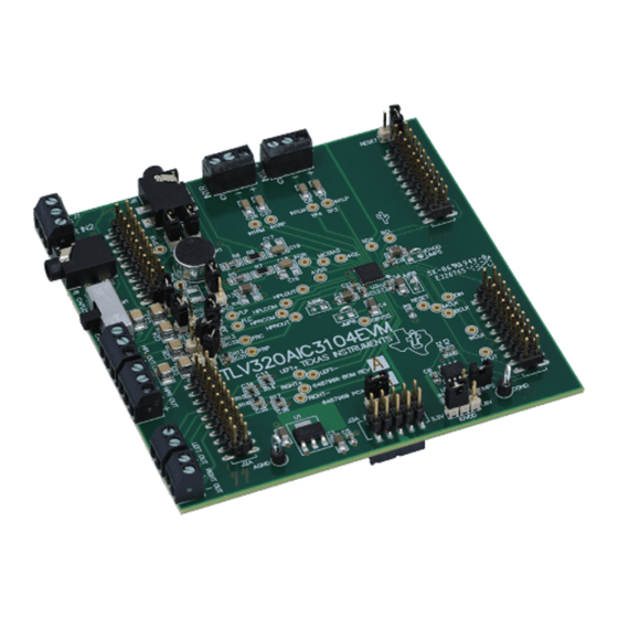
This user's guide describes the characteristics, operation, and use of the TLV320AIC3104EVM, both by itself and as part of the TLV320AIC3104EVM-PDK. This evaluation module (EVM) is a complete stereo audio codec with several inputs and outputs, extensive audio routing, mixing, and effects capabilities. A complete circuit description, schematic diagram, and bill of materials are also included. - Page 2 ....................Analog Interface Pinout ..................... Alternate Analog Connectors ..................... Digital Interface Pinout ....................... Power Supply Pinout ................... TLV320AIC3104EVM Bill of Materials ..................USB-MODEVM Bill of Materials ..............USB Control Endpoint HIDSETREPORT Request ....................Data Packet Configuration ....................GPIO Pin Assignments TLV320AIC3104EVM and TLV320AIC3104EVM-PDK SLAU218 –...
-
Page 3: Evm Overview
The USB-MODEVM has two EVM positions that allow for the connection of two small evaluation module or one larger evaluation module. The TLV320AIC3104EVM is designed to fit over both of the smaller evaluation module slots as shown below. - Page 4 C port realized using the TAS1020B, as well as the TAS1020B digital audio interface.. In the factory configuration, the board is ready to use with the TLV320AIC3104EVM. To view all the functions and configuration options available on the USB-MODEVM board, see the USB-MODEVM Interface Board schematic in Appendix E.
-
Page 5: Usb-Modevm Sw2 Settings
USB-MODEVM Table 1 provides a list of the SW2 settings on the USB=MODEVM. For use with the TLV320AIC3104EVM, SW-2 positions 1 through 7 should be set to ON, while SW-2.8 should be set to OFF. Table 1. USB-MODEVM SW2 Settings... - Page 6 5-6KINTERFACE or HPA-MCUINTERFACE, or to the USB-MODEVM Interface board if purchased as part of the TLV320AIC3104EVM-PDK. See the product folders on the TI Web site for these evaluation modules or the TLV320AIC3104 for a current list of compatible interface and/or accessory boards.
-
Page 7: Tlv320Aic3104Evm-Pdk Setup And Installation
Verify that all power supplies are within the safe operating limits shown on the TLV320AIC3104 data sheet before applying power to the EVM. J15 provides connection to the common power bus for the TLV320AIC3104EVM. Power is supplied on the pins listed in Table A-4. -
Page 8: Default Software Screen
TLV320AIC3104EVM-PDK Setup and Installation EVM Connections 1. Ensure that the TLV320AIC3104EVM is installed on the USB-MODEVM Interface board, aligning J13, J14, J15, J16, and J17 with the corresponding connectors on the USB-MODEVM. 2. Verify that the jumpers and switches are in their default conditions. -
Page 9: Device Selection Window
Figure 3. For operation with the TLV320AIC3104EVM, the user should select AIC3104 from the pulldown menu and click Accept. The software will take a few seconds to configure the software for operation before proceeding. A progress bar should appear and show the status of the configuration. - Page 10 For operation of the EVM in the default status, no changes are required on this panel. The default settings are A1=A0=0. Changes to this panel are only required when operating the EVM with a specific I C address (other than default) or when evaluating multiple EVM. TLV320AIC3104EVM and TLV320AIC3104EVM-PDK SLAU218 – August 2007 Submit Documentation Feedback...
- Page 11 AGC Gain Applied indicators use a bar graph to show the amount of gain which has been applied by the AGC, and indicators that light when the AGC is saturated. SLAU218 – August 2007 TLV320AIC3104EVM and TLV320AIC3104EVM-PDK Submit Documentation Feedback...
-
Page 12: Default Configuration Tab
The user can change to the Command Line Interface Tab (see Figure to view the actual settings that were programmed into the codec. Figure 6. Default Configuration Tab TLV320AIC3104EVM and TLV320AIC3104EVM-PDK SLAU218 – August 2007 Submit Documentation Feedback... -
Page 13: Audio Input Tab
In the upper right portion of this tab are controls for Weak Common Mode Bias. Enabling these controls will result in unselected inputs to the ADC channels to be weakly biased to the ADC common mode voltage. SLAU218 – August 2007 TLV320AIC3104EVM and TLV320AIC3104EVM-PDK Submit Documentation Feedback... -
Page 14: Bypass Paths
The active bypass paths allow the inputs to bypass the ADC and DAC functional blocks and be routed to the analog output mixers to be summed into the output amplifiers. TLV320AIC3104EVM and TLV320AIC3104EVM-PDK SLAU218 – August 2007 Submit Documentation Feedback... -
Page 15: Audio Interface Tab
If only one digital microphone is connected, then the remaining ADC can be used with an analog input signal from the analog input pins. Refer to section SLAU218 – August 2007 TLV320AIC3104EVM and TLV320AIC3104EVM-PDK Submit Documentation Feedback... - Page 16 WCLK are supplied to the codec externally). For use with the PC software and the USB-MODEVM, the default settings should be used; no change to the software are required. TLV320AIC3104EVM and TLV320AIC3104EVM-PDK SLAU218 – August 2007 Submit Documentation Feedback...
-
Page 17: Clocks Tab
CLKDIV_OUT, the PLL is not used; when set to PLLDIV_OUT, the PLL is used to generate the clocks. Note: Per the TLV320AIC3104 data sheet, the codec should be configured to allow the value of Fsref to fall between the values of 39 kHz to 53 kHz. SLAU218 – August 2007 TLV320AIC3104EVM and TLV320AIC3104EVM-PDK Submit Documentation Feedback... - Page 18 ADC or DAC by pressing the corresponding Dual Rate Mode button. The ADC and DAC sampling rates are shown in the box to the right of each control. TLV320AIC3104EVM and TLV320AIC3104EVM-PDK SLAU218 – August 2007...
-
Page 19: Gpio Tab
– If selected as a General Purpose Input, the state of the GPIO1 pin is reflected by the Input Level indicator. If selected as a General Purpose Output, the state of the GPIO1 pin can be set by using the Output Level button. SLAU218 – August 2007 TLV320AIC3104EVM and TLV320AIC3104EVM-PDK Submit Documentation Feedback... - Page 20 Output Level control sets the output state of the MFP2 pin either high or low. The states of the MFP0, MFP1 and MP3 inputs are indicated by the three indicator lights on the right-hand side of this group box. TLV320AIC3104EVM and TLV320AIC3104EVM-PDK SLAU218 – August 2007...
-
Page 21: Agc Tab
The Use advanced settings? button should be enabled to program the registers with the correct values selected via the pulldown options for base time and multiplier. SLAU218 – August 2007 TLV320AIC3104EVM and TLV320AIC3104EVM-PDK Submit Documentation Feedback... -
Page 22: Left Agc Settings
Noise gate functions, such as Hysteresis, Enable Clip stepping, Threshold (dB), Signal Detect Debounce (ms), and Noise Detect Debounce (ms) are set using the corresponding controls in the Noise Gate group box for each channel. TLV320AIC3104EVM and TLV320AIC3104EVM-PDK SLAU218 – August 2007 Submit Documentation Feedback... -
Page 23: Filters Tab
Note that the plot shows only the responses of the effect filters, not the combined response of those filter along with the de-emphasis and ADC high-pass filters. SLAU218 – August 2007 TLV320AIC3104EVM and TLV320AIC3104EVM-PDK Submit Documentation Feedback... -
Page 24: Adc High Pass Filters
The ADC digital outputs stream can be routed through the digital effects filter in the codec to allow custom audio performance. The digital effects filter cannot operate on both the ADC or DAC at the same time. The digital effects filter operation is discussed in Section 4.11.3 TLV320AIC3104EVM and TLV320AIC3104EVM-PDK SLAU218 – August 2007 Submit Documentation Feedback... -
Page 25: Dac Filters
DAC to allow custom audio performance. The digital effects filter cannot operate on both the ADC or DAC at the same time. The digital effects filter operation is discussed in Section 4.11.3 SLAU218 – August 2007 TLV320AIC3104EVM and TLV320AIC3104EVM-PDK Submit Documentation Feedback... -
Page 26: Enabling Filters
To use these filters, enter the gain desired and the corner frequency. Choose the mode to use (Bass or Treble); the response will be plotted on the Effect Filter Response graph. TLV320AIC3104EVM and TLV320AIC3104EVM-PDK SLAU218 – August 2007 Submit Documentation Feedback... -
Page 27: Eq Filters
Parameter entry boxes appropriate to the filter type will be shown (ripple, for example, with Chebyshev filters, etc.). Enter the desired design parameters and the response will be shown. (See Figure 23.) Figure 23. Analog Simulation Filters SLAU218 – August 2007 TLV320AIC3104EVM and TLV320AIC3104EVM-PDK Submit Documentation Feedback... -
Page 28: Preset Filters
25) for both biquads for both left and right channels. The filter response will not be shown on the Effect Filter Response graph for user filters. Figure 25. User Filters TLV320AIC3104EVM and TLV320AIC3104EVM-PDK SLAU218 – August 2007 Submit Documentation Feedback... -
Page 29: Effect Settings
The User Filters tab may be used to load the coefficients. Figure Figure 26. 3D Effect Settings To enable the 3D effect, check the 3D Effect On box. The Depth knob controls the value of the 3D Attenuation Coefficient. SLAU218 – August 2007 TLV320AIC3104EVM and TLV320AIC3104EVM-PDK Submit Documentation Feedback... -
Page 30: Output Stage Configuration Tab
The output Coupling control can be chosen as either Capless or AC-coupled. This setting should correspond to the setting of the hardware switch (SW1) on the TLV320AIC3104EVM. The common mode voltage of the outputs may be set to 1.35 V, 1.5 V, 1.65 V, or 1.8 V using the Common Mode Voltage control. - Page 31 The I C Bus Error Detection button allows the user to enable circuitry which will set a register bit (Register 107, D0) if an I C bus error is detected. SLAU218 – August 2007 TLV320AIC3104EVM and TLV320AIC3104EVM-PDK Submit Documentation Feedback...
-
Page 32: Dac/Line Outputs Tab
Line or HP outputs, these can be selected as choices in the Output Path control. Note that if the Line or HP outputs are selected as the Output Path, the mixer controls on this tab and the High Power Output tabs have no effect. TLV320AIC3104EVM and TLV320AIC3104EVM-PDK SLAU218 – August 2007 Submit Documentation Feedback... - Page 33 DAC_L and DAC_R levels can each be set to create a custom mix of signals presented to that particular line output. Note: if the DAC Output Path control is set to anything other than Mix with Analog Inputs, these controls have no effect. SLAU218 – August 2007 TLV320AIC3104EVM and TLV320AIC3104EVM-PDK Submit Documentation Feedback...
-
Page 34: High-Power Outputs Tab
At the right side of the output strip is a master volume knob for that output, which allows the output amplifier gain to be muted or set from 0 to 9 dB in 1-dB steps. TLV320AIC3104EVM and TLV320AIC3104EVM-PDK SLAU218 – August 2007... -
Page 35: Command Line Interface Tab
The log file is a standard text file that can be opened with any text editor, and looks much like the source script file, but with the additional information of the result of each script command executed. SLAU218 – August 2007 TLV320AIC3104EVM and TLV320AIC3104EVM-PDK Submit Documentation Feedback... -
Page 36: File Menu
TLV320AIC3104EVM software. Figure 31. File Menu Under the Help menu is an About... menu item which displays information about the TLV320AIC3104EVM software. The actual USB protocol used as well as instructions on writing scripts are detailed in the following subsections. -
Page 37: Analog Interface Pinout
A.1.1 Analog Dual-Row Header Details (J13 and J14) For maximum flexibility, the TLV320AIC3104EVM is designed for easy interfacing to multiple analog sources. Samtec part numbers SSW-110-22-F-D-VS-K and TSM-110-01-T-DV-P provide a convenient 10-pin dual row header/socket combination at J13 and J14. These headers/sockets provide access to the analog input and output pins of the device. -
Page 38: Alternate Analog Connectors
The stereo microphone input is also tied to J6 and the stereo headphone output (the HP set of outputs) is available at J7. Table A-2 summarizes the screw terminals available on the TLV320AIC3104EVM. Table A-2. Alternate Analog Connectors DESIGNATOR... -
Page 39: Digital Interface Pinout
Digital Interface Connectors (J16 and J17) Digital Interface Connectors (J16 and J17) The TLV320AIC3104EVM is designed to easily interface with multiple control platforms. Samtec part numbers SSW-110-22-F-D-VS-K and TSM-110-01-T-DV-P provide a convenient 10-pin dual row header/socket combination at J16 and J17. These headers/sockets provide access to the digital control and serial data pins of the device. -
Page 40: Power Supply Pinout
C is actually routed to both connectors; however, the device is connected only to J16. Power Supply Connector Pin Header, J15 J15 provides connection to the common power bus for the TLV320AIC3104EVM. Power is supplied on the pins listed in Table A-4. - Page 41 Appendix B Appendix B TLV320AIC3104EVM Schematic The schematic diagram for the modular TLV320AIC3104EVM is provided as a reference. SLAU218 – August 2007 TLV320AIC3104EVM Schematic Submit Documentation Feedback...
-
Page 42: Assembly Layer
MD9745APZ-F DATA ACQUISITION PRODUCTS MICROPHONE HIGH PERFORMANCE ANALOG DIVISION SEMICONDUCTOR GROUP 6730 SOUTH TUCSON BLVD., TUCSON, AZ 85706 USA TITLE ENGINEER RICK DOWNS TLV320AIC3104EVM DRAWN BY BOB BENJAMIN DOCUMENT CONTROL NO. 6487968 SIZE DATE 29-Nov-2006 SHEET FILE... -
Page 43: Layer 3
J3B (BOTTOM) = SAM_SSW-105-22-F-D-VS-K 24AA64I/SN JMP16 IOVDD JMP2 DATA ACQUISITION PRODUCTS HIGH-PERFORMANCE ANALOG DIVISION SEMICONDUCTOR GROUP 6730 SOUTH TUCSON BLVD., TUCSON, AZ 85706 USA TITLE ENGINEER RICK DOWNS TLV320AIC3104EVM INTERFACE DRAWN BY BOB BENJAMIN DOCUMENT CONTROL NO. 6487968 SIZE DATE 29-Nov-2006 SHEET FILE... -
Page 44: Silk Screen
Appendix C Appendix C TLV320AIC3104EVM Layout Views Figure C-1. Assembly layer Figure C-2. Top Layer TLV320AIC3104EVM Layout Views SLAU218 – August 2007 Submit Documentation Feedback... - Page 45 Appendix C Figure C-3. Layer 3 Figure C-4. Layer 4 SLAU218 – August 2007 TLV320AIC3104EVM Layout Views Submit Documentation Feedback...
- Page 46 Appendix C Figure C-5. Silk Screen Figure C-6. Bottom Layer TLV320AIC3104EVM Layout Views SLAU218 – August 2007 Submit Documentation Feedback...
-
Page 47: Tlv320Aic3104Evm Bill Of Materials
Appendix D Appendix D TLV320AIC3104EVM Bill of Materials The complete bill of materials for the modular TLV320AIC3104EVM is provided as a reference. Table D-1. TLV320AIC3104EVM Bill of Materials Value Ref Des Description Manufacturer Mfr Part Number R7, R8 1/4W 5% Chip Resistor... - Page 48 Appendix E Appendix E USB-MODEVM Schematic The schematic diagram for USB-MODEVM Interface Board (included only in the TLV320AIC3104EVM-PDK) is provided as a reference. USB-MODEVM Schematic SLAU218 – August 2007 Submit Documentation Feedback...
- Page 49 REVISION HISTORY ENGINEERING CHANGE NUMBER APPROVED IOVDD IOVDD IOVDD +3.3VD +3.3VD EXT MCLK ZXMN6A07F 2.7K 2.7K SN74LVC1G125DBV USB MCK MCLK USB I2S I2SDIN USB I2S ZXMN6A07F USB MCK BCLK EXTERNAL I2C USB SPI SN74LVC125APW LRCLK USB RST +3.3VD +3.3VD EXT MCK IOVDD I2SDOUT SW DIP-8...
- Page 50 REVISION HISTORY ENGINEERING CHANGE NUMBER APPROVED JMP5 A0(-) A0(+) CNTL GPIO0 A1(-) A1(+) CLKX DGND A2(-) A2(+) CLKR GPIO1 A3(-) A3(+) GPIO2 AGND DGND AGND GPIO3 AGND GPIO4 VCOM AGND REF- TOUT DGND +5VA J13A (TOP) = SAM_TSM-105-01-L-DV-P AGND REF+ GPIO5 J13B (BOTTOM) = SAM_SSW-105-22-F-D-VS-K DAUGHTER-ANALOG...
- Page 51 Appendix F Appendix F USB-MODEVM Bill of Materials The complete bill of materials for USB-MODEVM Interface Board (included only in the TLV320AIC3104EVM-PDK) is provided as a reference. Table F-1. USB-MODEVM Bill of Materials Designators Description Manufacturer Mfr Part Number 10Ω...
- Page 52 www.ti.com Appendix F Table F-1. USB-MODEVM Bill of Materials (continued) Designators Description Manufacturer Mfr Part Number JMP1–JMP4 2-position jumper, 0.1" spacing Samtec TSW-102-07-L-S JMP8–JMP14 2-position jumper, 0.1" spacing Samtec TSW-102-07-L-S JMP5, JMP6 3-position jumper, 0.1" spacing Samtec TSW-103-07-L-S JMP7 3-position dual row jumper, 0.1" spacing Samtec TSW-103-07-L-D SMT, half-pitch 2-position switch...
-
Page 53: Usb Control Endpoint Hidsetreport Request
www.ti.com Appendix G Appendix G USB-MODEVM Protocol USB-MODEVM Protocol The USB-MODEVM is defined to be a Vendor-Specific class, and is identified on the PC system as an NI-VISA device. Because the TAS1020 has several routines in its ROM which are designed for use with HID-class devices, HID-like structures are used, even though the USB-MODEVM is not an HID-class device. - Page 54 www.ti.com USB-MODEVM Protocol Do the same with a fast mode I C device: 0x12 0xA0 0x02 0x05 0xAA 0x55 Now with an SPI device which uses an 8-bit register address: 0x10 0xA0 0x02 0x05 0xAA 0x55 Now let's do a 16-bit register address, as found on parts like the TSC2101. Assume the register address (command word) is 0x10E0: 0x14 0x10 -->...
- Page 55 www.ti.com USB-MODEVM Protocol If the command is sent with no problem, the returning byte [0] should be the same as the sent one logically ORed with 0x20 - in our first example above, the returning packet should be: 0x31 0xA0 0x02 0x05 0xAA...
-
Page 56: Gpio Pin Assignments
www.ti.com GPIO Capability The return packet should be 0x21 0xA0 0x02 0x05 0xAA 0x55 assuming that the values we wrote above starting at Register 5 were actually written to the device. GPIO Capability The USB-MODEVM has seven GPIO lines. Access them by specifying the interface to be 0x08, and then using the standard format for packets—but addresses are unnecessary. - Page 57 www.ti.com Writing Scripts Each line in a script file is one command. There is no provision for extending lines beyond one line. A line is terminated by a carriage return. The first character of a line is the command. Commands are: Set interface bus to use Read from the serial control bus Write to the serial control bus...
- Page 58 www.ti.com Writing Scripts Here is an example of using an SPI device that requires 16-bit register addresses: # setup TSC2101 for input and output # uses SPI16 interface # this script sets up DAC and ADC at full volume, input from onboard mic # Page 2: Audio control registers w 10 00 00 00 80 00 00 00 45 31 44 FD 40 00 31 C4 w 13 60 11 20 00 00 00 80 7F 00 C5 FE 31 40 7C 00 02 00 C4 00 00 00 23 10 FE...
- Page 59 EVALUATION BOARD/KIT IMPORTANT NOTICE Texas Instruments (TI) provides the enclosed product(s) under the following conditions: This evaluation board/kit is intended for use for ENGINEERING DEVELOPMENT, DEMONSTRATION, OR EVALUATION PURPOSES ONLY and is not considered by TI to be a finished end-product fit for general consumer use. Persons handling the product(s) must have electronics training and observe good engineering practice standards.
- Page 60 TI as compliant with ISO/TS 16949 requirements. Buyers acknowledge and agree that, if they use any non-designated products in automotive applications, TI will not be responsible for any failure to meet such requirements. Following are URLs where you can obtain information on other Texas Instruments products and application solutions: Products...
Need help?
Do you have a question about the TLV320AIC3104EVM and is the answer not in the manual?
Questions and answers