Table of Contents
Advertisement
Quick Links
EC Declaration of Conformity
We
Iwill Corp.
No. 9-1, Kong 6th RD.,
Lin Kou 2nd Industrial
Park, Taipei, Taiwan R.O.C.
declare under sole responsibility that the
P6NS motherboard
meets the intent of Directive 89/336/ECC for Electromagnetic
Compatibility. Compliance was demonstrated to the following
specifications as listed in the official Journal of the European
Communities:
EN 50081-1 Emissions:
EN 55022
EN 55022
EN 60555-2
EN 50082-1 Immunity:
IEC 801-2
IEC 801-3
IEC 801-4
Radiated, Class B
Conducted, Class B
Power Harmonics
Electrostatic Discharge
RF Radiat
Fast Transient
i
Advertisement
Table of Contents

Related Manuals for IWILL P6NS


Summary of Contents for IWILL P6NS
- Page 1 Lin Kou 2nd Industrial Park, Taipei, Taiwan R.O.C. declare under sole responsibility that the P6NS motherboard meets the intent of Directive 89/336/ECC for Electromagnetic Compatibility. Compliance was demonstrated to the following specifications as listed in the official Journal of the European...
- Page 2 About This Manual This P6NS PPro SCSI Motherboard is the newest member to our SCSI Motherboard solution products families. It incorporated with new Intel generation 82440FX Chipset and with Adaptec new Ultra / Ultra Wide SCSI embedded which is equilevent to AHA 2940UW. Adaptec RAID port option ready is a big advantage in this P6NS PPro SCSI motherboard.
-
Page 3: Table Of Contents
Contents Chapter 1 - Overview Features ............P1 Chapter 2 - Quick Installation ........P5 Chapter 3 - Hardware Installation Prepare & Inspection ........P7 Placement ............P8 Block Diagram ..........P12 CPU group ............P13 Integrated PCI Bridge ........P15 SCSI Interf ace .......... -
Page 5: Chapter 1 - Overview
HAPTER 1 Overview Thank you for purchasing this P6NS PPro SCSI Motherboard. This operation manual will guide you to proper configure and install. It has an overview of the engineer design and feature of this board. Also, this manual provides useful information for your later upgrade or change the configuration. - Page 6 for businesses moving to 32-bit computing when using the 32-bit Operating System and Applications. ◼ Intel Pentium Pro Processor operating at 150 ~ 233 MHz with 387 ZIF socket 8 is scalable to accept faster Processors in the future. The Pentium Pro Processor is the next in the Intel386, Intel486, and Pentium family of processor.
- Page 7 Easy of use ◼ Floppy Interface: Support both 3 1/2" and 5 1/4" floppy disk drives and Tape Drive (360K / 720K/ 1.2M / 1.44M / 2.88MB) Enabled/Disable selectable from system BIOS Non-Burst Mode DMA Option ...
-
Page 8: Chapter 2 Quick Installation
HAPTER 2 Quick Installation... - Page 9 This SCSI Motherboard is shipped with manufacture preset at : CPU Clock at 200 MHz Adaptec Ultra Wide SCSI Chip Enabled Wide SCSI Mode Enabled SCSI Terminator Control by BIOS Printer ECP Mode at DMA3 Printer at IRQ7 , Address at 378h Serial 1 at IRQ4, Serial 2 at IRQ3 PS/2 MOUSE at IRQ 12 Reference to the Chapter 3 &...
-
Page 10: Chapter 3 - Hardware Installation
Step 7. Save the setup data to the CMOS Exit the "Setup Menu " screen and then write to CMOS RAM. And enjoy the high performance system board. Step 8. After boot your system O.S., insert the Ada ptec EZ-SCSI Installation diskette in a floppy disk drive and follow the EZ- SCSI operation manual or reference to Adaptec 7800 Family Set manual which will guide you to install theDOS/Windows,... - Page 11 PC prior to opening this bag. The P6NS PPro SCSI Motherboard, like all electronic equipment is static sensitive. Please take the proper precautions when handling the board. You should avoid static up, if possible, You should ground yourself by touching a metal table or your computer frame.
-
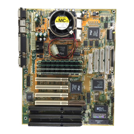
Page 12: Placement
The SMC 37C669 Super I/O controller provides the standard PC I/O function: floppy interface, two 16 Byte FIFO serial ports and EPP/ECP capable parallel port. The P6NS layout is shown in next page for user's reference. Care must be taken when inserting memory modules, inserting Pentium Pro processor CPU or even plugging PCI ca rd into associated slots to avoid damaging any circuits or sockets on board. - Page 13 The P6NS supports Onboard two PCI IDE connectors, and detects IDE harddisk type by BIOS utility automatically. The P6NS supports Award Plug & Play BIOS for the ISA and PCI cards. The BIOS can be located in Flash EPROM. The advantage of having Flash EPROM is...
- Page 14 JP12 JP17 Pentium 300 MHz Turbo LED Keylock SM I SW IDE LED SCSI LED Speaker Reset SW Rem ote Pow er On/Off Placement & Connector...
- Page 15 JP17 Pentium 300 MHz 3.3V from on-board regulator 3.3V from ATX pow er s upply JP8 : 1-2 For M om e ntary Sw itch 2-3For Toggle Sw itch JP16 & JP18 : SCSI Term inator JP11 : 1-2 Enable d SCSI JP11 JP18 2-3 Dis able d SCSI...
-
Page 16: Block Diagram
3.3 Block Diagram Pentium Pro Processor Family HOST Bus MD(63:0) MA(11:0) Main Memory MPE(7:0) Control PCI Bridge Data Bus & Memory Acclerator PD(15:0) Controller Control PCI Slots PCI Bus IDE CD-ROM PIIX3 Port A Port B IDE HDD I/O Bridge Adaptec Graphics Host SCSI... -
Page 17: Cpu Group
Once you match the hole with the pin 1, then gentle insert the CPU and press socket handle bar down. 3.4.2 System Memory Configuration The P6NS supports different type of settings for the system memory. There is no jumper nor connector needed for memory configuration. Bank 0 Single Side DRAM... -
Page 18: Integrated Pci Bridge
The memory size of any configuration can be combined flexibly. BIOS will detect your memory configurations and sizes automatically. 2. P6NS support Fast Page DRAM, EDO or BEDO DRAM SIMMs, but cannot be mixed within the same memory bank. -
Page 19: Scsi Interface
There are four interrupts in each PCI slot : INTA#, INTB#, INTC#, and INTD#. Since the P6NS adapts the PCI auto-configuration with the system BIOS Setup utility. When the system is turned on after adding a PCI add -in card, the BIOS automatically configure interrupts, DMA channels, I/O space, and other parameters. - Page 20 3.6.2 J26 Ultra SCSI Connector J26 is a 50 pins 8 bit internal Ultra SCSI connector. It attaches the SCSI cable(s) from this P6NS SCSI controller to the SCSI peripherals. The externa l SCSI port expansion kit is a optional for your connecting external devices.
- Page 21 Note: The 50 pin SCSI is an 8 bit SCSI bus, the 68 pin SCSI is a 16 bit SCSI bus which has a pin-to- pin connected to the 50 pins SCSI connector. Note: The SCSI termination must be on for the both side. The beginer and end must set the terminator on - otherwise the SCSI bus will not operate properly.
- Page 22 3.6.5 Set SCSI IDs You must assign a different SCSI ID to each device on the SCSI bus connected to the P6NS system board. See your SCSI device documentation for directions on how to determine the ID and change it.
-
Page 23: Adaptec Raidport Option
JP16&JP18 are both 3 pin jumper connectors. These are for Low/ High Byte SCSI Terminator. Function JP18 Note Low Byte SCSI Terminator Always On Low Byte SCSI Terminator Always Off Low Byte SCSI Terminator Controlled by BIOS *Default Function JP16 Note High Byte SCSI Terminator Always On *Default... -
Page 24: Ide Interface
Pe ntium RAID Port P6NS 3.8 IDE Interface 3.8.1 Primary, Secondary IDE Connectors Primary / Secondary IDE are 40 pins internal IDE port connectors. Use a 40 pins flat cable to connect between this connector and the IDE devices. Normally put the boot-up hard disk at the primary IDE channel and other IDE devices at the secondary IDE channel (like CD-ROM). -
Page 25: Enhanced Multi-Io
J22 is a 34 pins internal Floppy port connector. Use 34 pins flat cable to connect between this connector and floppy drives. Pe ntium 3.10.2 J2 Printer Connector J2 is a standard 25 pin external D-Sub connector. Pentium P6NS Following selection is all controled by the BIOS:... -
Page 26: Other
ECP Mode DMA Channel Select by BIOS printer Port Address and IRQ Select by BIOS (378h/3BC with IRQ7, 278h with IRQ5.) Printer and IEEE 1284 cable The IEEE 1284 compliant cables have better features on the following: ⚫ Twisted pairs of conductors ⚫... - Page 27 P6NS 3.11.2 Power Supply Connector There are two types of power connector provided by this SCSI motherboard. The 20 pin box header is ATX standard power connector. (will describe this on next chaptor ATX Form Factor). The 12-pin is AT standard power connectors. This is used to connect power lines and power good signal from the power supply's P8 and P9 headers to the motherboard.
- Page 28 Pentium Turbo LED Keylock SM I SW IDE LED SCSI LED Speaker Reset SW Note : This mainbaord has no Turbo function, it will not support Turbo switch. The Turbo LED will light-on when you connect a computer case that mounted Turbo LED and power on this system.
-
Page 29: Chapter 4 - Atx Form-Factor Overview
HAPTER 4 ATX Form-Factor Overview The P6NS has been designed with ATX form -factor. The board size is 12" x 9.6" (305mm x 244mm). The ATX from -factor improves over Baby AT and LPX in a number of ways. By using the ATX chassis then the power supply orientation and... - Page 30 IDE/ FDD connectors close to peripherals bays The P6NS is equipped with a standard I/O back pannel, featuring a serial port, PS/2 mouse port, PS/2 keyboard port, parallel port, and secondary serial port. The P6NS Supports two power input connectors. Two 6-PIN connectors (for AT power supply) and a single 20-PIN connectors (for ATX power supply).
- Page 31 Power Supply Pentium System On/Off switch ATX Power Supply Connector : Single Name Single Name 3.3V 3.3V -12.0V 3.3V PS-ON 5.0V 5.0V -5.0V PW-OK 5.0V 5VSB 5.0V 12.0V...
- Page 32 This P6NS SCSI motherboard supports a on-board regulator to support the 3.3V power for the motherboard Chipset. User can choose a regular Switching Power Supply that doesn’t support 3.3V for this motherboard. For the power On/Off switch control, through the JP7 is a 2 pin connector.
-
Page 33: Chapter 5 Award Bios Setup
HAPTER 5 Award BIOS Setup Notice The information in this guide is subject to change without notice. The software described in this guide is furnished under a license agreement and may be used or copied only in accordance with the terms of the agreement. Award Software, Inc. - Page 34 Introduction This section discusses Award's Setup program built into the ROM BIOS. The Setup program allows users to modify the basic system configuration. This special information is then stored in battery-backed RAM so that it retains the Setup information when the power is turned off. The Award BIOS installed in your computer system ROM (Read Only Memory) is a custom version of an industry standard BIOS.
- Page 35 press the keys at the correct time and the system does not boot, an error message will be displayed and you will again be asked to... Press <F1> To Continue, <Del> To Enter Setup. Using Setup In general, you use the arrow keys to highlight items, press <Enter> to select, use the PageUp and PageDown keys to change entries, press <F1>...
-
Page 36: Main Menu
Getting Help Press F1 to pop up a small help window that describes the appropriate keys to use and the possible selections for the highlighted item. To exit the Help Window press <Esc> or the F1 key again. In Case of Problems If, after making and saving system changes with Setup, you discover that your computer no longer is able to boot, the Award BIOS supports an override to the CMOS settings which resets your system to its defaults. - Page 37 Once you enter the Award BIOS CMOS Setup Utility, the Main Menu will appear on the screen. The Main Menu allows you to select from several setup functions and two exit choices. Use the arrow keys to select among the items and press <Enter>...
- Page 38 Change, set, or disable password. It allows you to limit access to the system and Setup, or just to Setup. Chipset Features Setup This setup page includes all the items of chipset special features. Power Management Setup This entry only appears if your system supports Power Management, screen PC”, standards.
- Page 39 HDD Low Level Format If supported by your system, this provides a hard disk low level format utility. Save & Exit Setup Save CMOS value changes to CMOS and exit setup. Exit Without Save Abandon all CMOS value changes and exit setup.
-
Page 40: Standard Cmos Setup
5.2 Standard CMOS Setup The items in Standard CMOS Setup Menu are divided into 10 categories. Each category includes no, one or more than one setup items. Use the arrow k eys to highlight the item and then use the <PgUp> or <PgDn> keys to select the value you want in each item. - Page 41 The time format is <hour> <minute> <second>. The time is calculated based on the 24-hour military-time clock. For example, 1 p.m. is 13:00:00. Daylight saving The category adds one hour to the clock when daylight-saving time begins. also subtracts one hour when standard time returns. Enabled Enable daylight-saving Disabled...
- Page 42 HEADS number of heads PRECOMP write precom LANDZONE landing zone SECTORS number of sectors MODE mode type Drive A Type / Drive B Type If a hard disk has not been installed Select NONE and press <Enter>. The category identifies the types of floppy disk drive A or drive B that have been installed in the computer.
- Page 43 All errors The system boot will not be stopped for any error that may be detected. All, The system boot will not stop for a keyboard error; it will But Keyboard stop for all other errors. All, But Diskette The system boot will not stop for a disk error; it will stop for all other errors.
-
Page 44: Bios Features Setup
5.3 BIOS Features Setup This section allows you to configure your system for basic operation. You have the opportunity to select the system default speed, boot -up sequence, keyboard operation, shadowing and security. ROM / PCI ISA BIOS BIOS FEATURES SETUP AWARD SOFTWARE, INC. - Page 45 ! WARNING ! Disk boot sector is to be modified Type "Y" to accept write or "N" to abort write Award Software, Inc. Enabled Activates automatically when the system boots up causing a warning message to appear when anything attempts to access the boot sector or hard disk partition table.
- Page 46 Boot Sequence This category determines which drive to search first for the disk operating system (i.e., DOS). Default value is A,C. System will first search for hard disk drive then floppy disk drive. System will first search for floppy disk drive then hard disk drive.
- Page 47 Boot Up NumLock Status This allows you to determine the default state of the numeric keypad. By default, the system boots up with NumLock on. Keypad is number keys Keypad is arrow keys Boot Up System Speed Selects the default system speed -- the normal operating speed at power up. High Set the speed to high Set the speed to low...
- Page 48 Enabled Enable typematic rate Disabled Disable typematic rate Typematic Rate (Chars/Sec) When the typematic rate is enabled, this selection allows you select the rate at which the keys are accelerated. 6 characters per second 8 characters per second 10 characters per second 12 characters per second 15 characters per second 20 characters per second...
- Page 49 Setup The system will boot, but access to Setup will be denied if the correct password is not entered at the prompt. Note: To disable security, select PASSWORD SETTING at Main Menu and then you will be asked to enter password. Do not type anything and just press <Enter>, it will disable security.
-
Page 50: Chipset Features Setup
5.4 Chipset Features Setup ROM PCI / ISA BIOS CHIPSET FEATURES SETUP AWARD SOFTWARE, INC. Auto Configuration : Enabled 8 Bit I/O Recovery Time 16 Bit I/O Recovery Time DRAM Speed Selection :60ns Memory Hole AT 15M-16M : Disabled DRAM RAS# Precharge Time MA Additional Wait state : Disabled RAS# To Cas# Delay... - Page 51 Auto Configuration Pre-defined values for DRAM, cache.. timing according to CPU type & system clock. The Choice: Enabled, Disabled. Note: When this item is enabled, the pre-defined items will become SHOW- ONLY. DRAM Timing The DRAM timing is controlled by the DRAM Timing Registers. The timings programmed into this register are dependent on the system design.
- Page 52 This sets the number of CPU clocks allowed before reads and writes to DRAM are performed. Seven clocks leadoff for reads and six clocks leadoff for writes. Six clocks leadoff for reads and five clocks leadoff for writes. 7/6 Leadoff timing is the default. Fast RAS# to CAS# Delay When DRAM is refreshed, both rows and columns are addressed separately.
- Page 53 x222 Write DRAM timings are 2-2-2-2 x333 Write DRAM timings are 3-3-3-3 x444 Write DRAM timings are 4-4-4-4 x222 timings is the default. Turbo Read Leadoff The turbo read leadoff may be required in certain system designs to support layouts or faster memories. Disabled is the default.
- Page 54 ISA Clock This item allows you to select the PCI clock type. PCI CLK/3 PCI clock type PCI CLK/4 PCI clock type Cache Features System BIOS Cacheable When enabled, accesses to the system BIOS ROM addressed at F0000H -FFFFFH are cached, provided that the cache controller is enabled. Enabled BIOS access cached Disabled...
- Page 55 takes place because the CPU is operating so much faster than the input/output bus that the CPU must be delayed to allow for the completion of the I/O. This item allows you to determine the recovery time allowed for 8 bit I/O. Choices are from NA, 1 to 8 CPU clocks.
- Page 56 When disabled, the chipset behaves as if it were the earlier DRAM ECC/PARITY Select This item allows you to select between two methods of DRAM error checking, ECC and Parity (default). Memory Parity / ECC Check This item allows you to select between three methods of memory error checking, Auto, Enabled and Disabled Single Bit Error Report...
- Page 57 This item allows you to select two timing of pipeline cache, Faster and Fastest.
-
Page 58: Power Management Setup
5.5 Power Management Setup The Power Management Setup allows you to configure you system to most effectively save energy while operating in a manner consistent with your own style of computer use. ROM PCI / ISA BIOS POWER MANAGEMENT SETUP AWARD SOFTWARE, INC. - Page 59 Min. Power Saving Minimum power management. Doze Mode = 1 hr. Standby Mode = 1 hr., Suspend Mode = 1 hr., and HDD Power Down = 15 min. Max. Power Saving Maximum power management -- ONLY AVAILABLE FOR SL CPU. Doze Mode = 1 min., Standby Mode = 1 min., Suspend Mode = 1 min., and HDD Power Down = 1 min.
- Page 60 Doze Mode When enabled and after the set time of system inactivity, the CPU clock will run at slower speed while all other devices still operate at full speed. Standby Mode When enabled and after the set time of system inactivity, the fixed disk drive and the video would be shut off while all other devices still operate at full speed.
-
Page 61: Pnp/Pci Conf Iguration
• IRQ5 (LPT 2) • IRQ6 (Floppy Disk) • IRQ7 (LPT 1) • IRQ8 (RTC Alarm) • IRQ9 (IRQ2 Redir) • IRQ10 (Reserved) • IRQ11 (Reserved) • IRQ12 (Reserved) • IRQ13 (Coprocessor) • IRQ14 (Hard Disk) • IRQ15 (Reserved) 5.6 PnP/ PCI Configuration Setup This section describes configuring the PCI bus system. - Page 62 components. This section covers some very technical items and it is strongly recommended that only experienced users should make any changes to the default settings. ROM PCI / ISA BIOS POWER MANAGEMENT SETUP AWARD SOFTWARE, INC. Resources Controlled by : Manual PCI IRQ Actived By : Level Reset Configuration Date...
- Page 63 Choices are Enabled and Disabled (default). IRQ3/4/5/7/9/10/11/ 12/14/15, DMA0/1/3/5/6/7 assigned to This item allows you to determine the IRQ / DMA assigned to the ISA bus and is not available to any PCI slot. Choices are Legacy ISA and PCI/ISA PnP. PCI IRQ Activated This sets the method by which the PCI bus recognizes that an IRQ service is being requested by a device.
-
Page 64: Integrated Peripherals
Award's ROM BIOS provides a built-in Setup program which allows user modify the system configuration and hardware parameters. The modified data will be stored in a battery-backed CMOS RAM, so data will be retained even the system power is off. In general, you are not required to change any data. Unless there is a conflict or you re-configuring system, this will need to enter new setup information. - Page 65 Onboard FDC Controller : Enabled Onboard UART 1 : 3F8/IRQ4 Onboard UART 2 : 2F8/IRQ3 → : Select Item Onboard UART 2 Mode : Standard ESC : Quit → : Select Item ESC : Quit F1 : Help PU/PD/+/- : Modify F5 : Old Values (Shift) F2...
- Page 66 BIOS to tell the controller what it wants and then let the controller and the C PU perform the complete task by themselves. This simpler and more efficient (and faster). Your system supports five modes, numbered from 0 (default) to 4, which primarily differ in timing.
-
Page 67: Load Setup Defaults
4.8 LOAD SETUP DEFAULTS The chipset defaults are settings which provide for maximum system performance. While Award has designed the custom BIOS to maximize performance, the manufacturer has the right to change these defaults to meet their needs. 4.9 Supervisor/User Password Setting You can set either supervisor or user password, or both of th em. -
Page 68: Hdd Low Level Format
Automatically detect and configure hard disk parameters. The Award BIOS includes this ability in the event you are uncertain of your hard disk parameters. 4.11 HDD LOW LEVEL FORMAT If supported by your system, this provides a hard disk low level format utility. 4.12 SAVE &... - Page 69 JP12 JP17 Pentium 300 MHz On-Board PCI-SCSI Turbo LED Keylock SM I SW IDE LED SCSI LED Speaker Reset SW Pow er On/Off Placement & Connector...
Need help?
Do you have a question about the P6NS and is the answer not in the manual?
Questions and answers