Table of Contents
Advertisement
Quick Links
EC Declaration of Conformity
We
Iwill Corp.
No. 10, Wu Chuan 3rd Rd.,
Hsin Chuang City, Taipei,
Taiwan, R.O.C.
Declare under sole responsibility that the
P55XPlus motherboard
Meets the intent of Directive 89/336/ECC for Electromagnetic Compatibility.
Compliance was demonstrated to the following specifications as listed in the official
Journal of the European Communities:
EN 50081-1 Emissions:
EN 50082-1 Immunity:
EN 55022
Radiated, Class B
EN 55022
Conducted, Class B
EN 60555-2 Power Harmonics
IEC
801-2
IEC
801-3
1
Electrostatic Discharge
RF Radiat
TM
Advertisement
Table of Contents

Related Manuals for IWILL P55XPLUS


Summary of Contents for IWILL P55XPLUS
- Page 1 Hsin Chuang City, Taipei, Taiwan, R.O.C. Declare under sole responsibility that the P55XPlus motherboard Meets the intent of Directive 89/336/ECC for Electromagnetic Compatibility. Compliance was demonstrated to the following specifications as listed in the official Journal of the European Communities:...
- Page 2 801-4 Fast Transient...
- Page 3 About This Manual This manual will guide the user on how this P55XPlus Ultra ATA ( Ultra DMA 33 ) motherboard is manufactured. All useful informations will be described in later chapters. Keep this manual for your future upgrade or system configuration change.
- Page 4 All other trademarks are owned by their respective owners. Copyright Copyright 1997 IWILL Corporation. All right reserved. No part of this publication may be reproduced, stored in a retrieval tape, disk, system, or transmitted in any form or by any means, electronic, mechanical, photocopying, recording or otherwise, without the prior written consent of IWILL USA Corporation.
-
Page 6: Table Of Contents
Contents CHAPTER 0........................8 QUICK INSTALL ATION ..................8 CHAPTER 1........................ 16 OVERVIEW........................ 16 1.1 F ......................16 EATURES 1.2 S ....................20 PECIFICATIONS CHAPTER 2........................ 21 HARDWARE INSTALL ATION................21 2.1 P ................ 21 REPARATION AND NSPECTION 2.2 P ...................... -
Page 8: Chapter 0
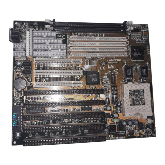
If you are a beginner and need to know more about this motherboard, please start from Chapter 1. COM1 BIOS COM2 P. IDE S. IDE DIMM1 DIMM2 SIMM1 SIMM2 SIMM3 SIMM4 F. Panel Figure 1:Connectors for P55XPlus... - Page 9 C200+ Figure 2: Jumpers Location...
- Page 10 Connector Function Description 12 pin Standard AT power input connector BIOS BIOS (Basic Input Output System) COM1 2 x 5 pin box-header for Serial 1 port connector COM2 2 x 5 pin box-header for Serial 2 port connector 321 pin Socket 7 CPU socket DIMM1 64 bit Dual In-line Memory Module.
- Page 11 Jumper Setting Part of ATX Power supply connector CMOS Clear Jumper CPU Voltage Monitor Jumper CPU Frequency select CPU Voltage Select Quick Installation Step 1. Install CPU Pull up the CPU handle bar, place the CPU into the socket in gentle and horizontal way then pull down the handle bar back to its original place.
- Page 12 Jumper JP6 is designed for users to set the proper voltage for the processor installed. A wrong voltage setting will damage the CPU permanently. There are total 6 different voltage selections in this P55XPlus motherboard to support full socket 7 processors that are avaialble today and in the near future.
- Page 13 Step 5. Install the Memory Module At least one piece of 72 pin SIMM(Single In-line Memory Module) or one piece of 168 pin DIMM(Dual In-line Memory Module ) must be inserted in this P55XPlus Ultra DMA 33 motherboard. The memory in this motherboard is devided into three banks.
- Page 14 The colored side of the flat cable is Pin 1. Step 7. Install the External Peripherals The external devices mean devices that are outside the computer chassis like the Serial mouse, Printer, PS/2 Mouse, External Modem and etc. Enclosed in this motherboard’s package, there are two 10 pin connectors: one converts to 9 pin ,and the other converts to 25 pin D-Sub male connector cable for Serial port.
- Page 15 Step 9. Connect the Keylock (keyboard lock) Switch Most computer chassis will provide a keylock switch. Normally, connect the marked keylock connector to this motherboard’s keylock connector. This will cause the keyboard out of function once you switch the keylock to “Lock.” This will prevent any un-authorized keyin.
-
Page 16: Chapter 1
Level Cache onboard that is well prepared to run heavy application. To run faster bus speed is a great plus in this P55XPlus motherboard. It not only can run the 66MHz bus that Intel claims on all her highest system bus but also built in 75MHz and 83MHz bus speed as an option for users to take advantage of. - Page 17 It fully supports plug and play I/O that contains two high speed serial ports, one ECP/EPP printer port, up to 2.88 floppy disk port, and keyboard. And the real time clock is used for users to enjoy the plug and play function. This Pentium EIDE, Ultra DMA 33 motherboard is designed with AT form factor to improve the easy access memory module, long add-on card support and some of the new features that traditional AT form factor can not achieved.
- Page 18 2 X 168-pin DIMM (Dual In Line Memory Module) (Rev 1.1) Support system memory up to 512MB (minimum of 8MB ) on board with either fast page mode, EDO under SIMM socket or the new Synchronous DRAM with DIMM socket (3.3V un-buffered type). Support 32 bit power-on function.
-
Page 20: Specifications
◼Floppy Interface: Support both 3 1/2" and 5 1/4" floppy disk drives and Tape Drive (360K / 720K/ 1.2M / 1.44M / 2.88MB) Enabled/Disable selectable from system BIOS Non-Burst Mode DMA Option,16 Byte Data FIFO ◼Serial Port: Two onboard 10 pin box-header connectors provide 2 Serial ports. Use the two cables that go with this motherboard to convert to the standard 9 and 25 pins D-Sub connectors. -
Page 21: Chapter 2
Hardware Installation 2.1 Preparation and Inspection This P55XPlus Ultra DMA 33 Motherboard, like all electronic equipments, is static sensitive. Please take the proper precautions when handling this board. You should avoid static up. If possible, You should ground yourself by touching a metal table or your computer frame. -
Page 22: Placement
2.2 Placement COM1 BIOS COM2 P. IDE S. IDE DIMM1 DIMM2 SIMM1 SIMM2 SIMM3 SIMM4 F. Panel Figure 1 : Connectors for P55XPlus... - Page 23 C200+ Figure 2 : Jumpers for P55XPlus...
-
Page 24: Cpu Group
2.3 CPU group 2.3.1 CPU Socket This CPU socket provides flexibility for Intel Pentium, Pentium OverDrive, Pentium with MMX processors, AMD K6 with MMX, K5-5k86 and Cyrix M2 with MMX, M1- 6x86 processors. When you install the CPU into the Zero Insertion Force ( ZIF ) socket, you should be very careful. - Page 25 2.3.2 JP4 CPU Cooler Fan Power Connector Warning !!! Warning !!! Warning !!! CPU Cooler is required to be placed on top of the CPU all the time to prevent CPU from over-heat. The CPU fan power is a 1 x 3 pin connector. Metal Latch To JP4 To Cabinet's speaker...
- Page 26 2.3.3 CPU Clock Select (JP5) JP5 is a 2 X 11 pin jumpers, with one "colored" jumper cap on it. One and only one jumper cap need to be put on this connector for selecting the CPU clock. Just put the colored yellow jumper cap to the speed your CPU really is.
- Page 27 (2) Cyrix CPU (for M1,M2) C200+ Cyrix 6x86 L-PR200+ CPU at 150 MHz (3) AMD CPU (K5,K6) (4) IDT C200+ C200+ IDT C6-200 IDT C6-150 CPU at 200 MHz CPU at 150 MHz...
- Page 28 * Refer to Appendix A for CPU voltage setting. 2.3.4 CPU Voltage (JP6) The manufacture default on this JP6 jumper is “2.8V.” This JP6 jumper sets the voltage for the CPU. For example, the Intel Pentium single voltage CPU uses 3.52V. and the Pentium with MMX CPU uses the dual power source and more “Green”...
-
Page 29: L2 Cache Memory
This motherboard provides two DIMMs and four SIMMs memory sockets. At least one piece 72 pin SIMM (Single In-line Memory Module) or one piece 168 pin DIMM (Dual In-line Memory Module)must be inserted in this P55XPlus Ultra DMA 33 motherboard. Two DIMM (DIMM 1, DIMM 2) sockets—support 3.3V Unbuffered Synchronous DRAM (SDRAM). -
Page 30: Ide Interface
Install the DIMM 2.6 IDE Interface 2.6.1 Primary, Secondary IDE Connectors Primary / Secondary IDE are 40 pins internal IDE port connectors. Use a 40-pin flat cable to connect between this connector and the IDE devices. Normally put the boot- up hard disk at the primary IDE channel and other IDE devices at the secondary IDE channel (like CD-ROM). -
Page 31: Usb (Universal Serial Bus)
Secondary IDE Primary IDE 3.6.2 IDE LED A 2 pin IDE detect LED connector. 2.7 USB (Universal Serial Bus) Basically, the USB is suitable for mid-to-low speed devices like Mouses, Keyboards, Joysticks..etc. In the past, all these were using different connectors, and it is complicated for end users to installthe system. -
Page 32: Enhanced Multi-Io
This USB riser card transfer rate is up to 12Mbit per second and will provide better performance compared to a cable type USB. J10 is a 2 x 10 pin connector, please connect it with the USB riser card and fix on the computer chassis’s backplane. - Page 33 2.8.2 Parallel Port Connector The parallel port is using the parallel signal transfer. The speed is faster than serial port and mostly it is used on the parallel printer or other parallel devices. Parallel port is a 25 pin female external DB25 connector for parallel port. Parallel Following selection is all controlled by the BIOS: ECP Mode DMA Channel Selected by BIOS...
-
Page 34: Others
Controlled impedance -- 62 ohm Limited cross-talk With these features, it will guarantee the IEEE 1284 cable perform at much higher bandwidth rates that the fast Centronics, EPP, and ECP modes perform at. If you are using the ordinary parallel cables running at the EPP or ECP mode that this controller provide, you may experience the data efforts. - Page 35 2.9.2 Power Supply Connector The 12-pin is AT standard power connectors. This is used to connect power lines and power good signal from the power supply's P8 and P9 headers to the motherboard. The pin assignments for P8 and P9 are indicated below: Note: The standard AT power supply will not power-up from JP12 for it doesn’t has the “POWER O.K.”...
- Page 36 Note: The Power LED can be connected from both the “LED” & “Keylock.” This motherboard has no Turbo function, so it will not support Turbo function. If the computer chassis has the front Turbo LED in the front panel for identification, The Power LED will light-on when you connect a computer case that has mounted Turbo LED and power on this system.
- Page 37 PS/2 Mouse PS/2 Mouse is a 6 pin Mini-DIN PS/2 mouse connector, the manufacture default is IRQ12. 2.9.5 CMOS Clear Jumper The JP1 is a 3 pin pin-header connector: jumper cap on 1-2 for normal operation or jumper cap on 2-3 for clear CMOS.
-
Page 38: Chapter 3
CHAPTER 3 Award BIOS Setup Notice The information in this manual is subject to change without notice. The software described in this guide is furnished under a license agreement and may be used or copied only in accordance with the terms of the agreement. Award Software, Inc. - Page 39 Starting Setup The Award BIOS is immediately activated when you first power on the computer. The BIOS reads the system information contained in the CMOS and begins the process of checking out the system and configuring it. When it finishes, the BIOS will seek an operating system on one of the disks and then launch and turn control over to the operating system.
- Page 40 - key Decrease the numeric value or make changes F1 key General help, only for Status Page Setup Menu and Option Page Setup Menu (Shift)F2 key Change color from total 16 colors. F2 to select color forward, (Shift) F2 to select color backward F3 key Calendar, only for Status Page Setup Menu F4 key...
-
Page 41: Main Menu
3.1 Main Menu Once you enter the Award BIOS CMOS Setup Utility, the Main Menu will appear on the screen. The Main Menu allows you to select from several setup functions and two exit choices. Use the arrow keys to select among the items and press <Enter> to accept and enter the sub-menu. - Page 42 This setup page includes all the items of chipset special features. Power Management Setup This entry only appears if your system supports Power Management, screen PC”, standards. PNP / PCI Configuration Setup This entry appears if your system supports PNP / PCI. Integrated Peripherals This section page includes all the items of IDE hard drive and Programmed Input / Output features.
-
Page 43: Standard Cmos Setup
3.2 Standard CMOS Setup The items in Standard CMOS Setup Menu are divided into 10 categories. Each category includes no, one or more than one setup items. Use the arrow keys to highlight the item and then use the <PgUp> or <PgDn> keys to select the value you want in each item. - Page 44 Daylight saving The category adds one hour to the clock when daylight-saving time begins. It also subtracts one hour when standard time returns. Enabled Enable daylight-saving Disabled Disable daylight-saving Primary Master / Primary Slave / Secondary Master / Secondary Slave The categories identify the types of 2 channels that have been installed in the computer.
- Page 45 None No floppy drive installed 360K, 5.25 in 5-1/4 inch PC-type standard drive; 360 kilobyte capacity 1.2M, 5.25 in 5-1/4 inch AT-type high-density drive; 1.2 megabyte capacity 720K, 3.5 in 3-1/2 inch double-sided drive; 720 kilobyte capacity 1.44M, 3.5 in 3-1/2 inch double-sided drive;...
-
Page 46: Bios Features Setup
Base Memory The POST will determine the amount of base (or conventional) memory installed in the system. The value of the base memory is typically 512K for systems with 512K memory installed on the motherboard, or 640K for systems with 640K or more memory installed on the motherboard. - Page 47 Virus Warning When this item is enabled, the Award BIOS will monitor the boot sector and partition table of the hard disk drive for any attempt at modification. If an attempt is made, the BIOS will halt the system and the following error message will appear. Afterwards, if necessary, you will be able to run an anti-virus program to locate and remove the problem before any damage is done.
- Page 48 System will first search for hard disk drive then floppy disk drive. System will first search for floppy disk drive then hard disk drive. CDROM,C,A System will first search for CDROM drive, then hard disk drive and then floppy disk drive. C,CDROM, A System will first search for hard disk drive , then CDROM drive, and then floppy disk drive.
- Page 49 Typematic Rate Setting This determines if the typematic rate is to be used. When disabled, continually holding down a key on your keyboard will generate only one instance. In other words, the BIOS will only report that the key is down. When the typematic rate is enabled, the BIOS will report as before, but it will then wait a moment, and, if the key is still down, it will begin the report that the key has been depressed repeatedly.
- Page 50 Note: To disable security, select PASSWORD SETTING at Main Menu and then you will be asked to enter password. Do not type anything and just press <Enter>, it will disable security. Once the security is disabled, the system will boot and you can enter Setup freely.
-
Page 51: Chipset Features Setup
3.4 Chipset Features Setup ROM PCI/ISA BIOS (XXXXXXXX) CHIPSET FEATURES SETUP AWARD SOFTWARE, INC. Auto Configuration Enabled Passive Release : Disabled AT BUS CLOCK 7.16 MHz ISA :ome Buffer Disabled DRAM Write WS :X-3-3-3 Delay Transaction Disabled Page Mode Read WS X-4-4-4 8 bit TAG RAM Size... - Page 52 DRAM Settings The first chipset settings deal with CPU access to dynamic random access memory (DRAM). The default timings have been carefully chosen and should only be altered if data is being lost. Such a scenario might well occur if your system had mixed speed DRAM chips installed so that greater delays may be required to preserve the integrity of the data held in the slower memory chips.
- Page 53 DRAM R/W Leadoff Timing This sets the number of CPU clocks allowed before reads and writes to DRAM are performed. Seven clocks leadoff for reads and six clocks leadoff for writes. Six clocks leadoff for reads and five clocks leadoff for writes. 7/6 Leadoff timing is the default.
- Page 54 Turbo Read Leadoff The turbo read leadoff may be required in certain system designs to support layouts or faster memories. Disabled is the default. DRAM Speculative Leadoff The ALI Aladdin 4+ chipset is capable of allowing a DRAM read request to be generated slightly before the address has been fully decoded.
- Page 55 Enabled Video BIOS access cached Disabled Video BIOS access not cached Disabled is the default. PCI and IDE Configuration Bit I/O Recovery Time The recovery time is the length of time, measured in CPU clocks, which the system will delay after the completion of an input/output request. This delay takes place because the CPU is operating so much faster than the input/output bus that the CPU must be delayed to allow for the completion of the I/O.
- Page 56 Memory Parity / ECC Check This item allows you to select between three methods of memory error checking, Auto, Enabled and Disabled Single Bit Error Report L2 Cache Cacheable Size When a single bit error is detected, the offending DRAM row ID is latched . The latched Valued is held until software explicit clears the error status flag.
-
Page 57: Power Management Setup
3.5 Power Management Setup The Power Management Setup allows you to configure you system to most effectively save energy while operating in a manner consistent with your own style of computer ROM PCI/ISA BIOS (XXXXXXXX) POWER MANAGEMENT SETUP AWARD SOFTWARE, INC. Power Management Enabled **Power Down &... - Page 58 Disable (default) No power management. Disables all four modes Min. Power Saving Minimum power management. Doze Mode = 1 hr. Standby Mode = 1 hr., Suspend Mode = 1 hr., and HDD Power Down = 15 min. Max. Power Saving Maximum power management -- ONLY AVAILABLE FOR SL CPU.
- Page 59 Suspend Mode When enabled and after the set time of system inactivity, all devices except the CPU will be shut off. HDD Power Down When enabled and after the set time of system inactivity, the hard disk drive will be powered down while all other devices remain active.
-
Page 60: Pnp/ Pci Configuration Setup
3.6 PnP/ PCI Configuration Setup This section describes configuring the PCI bus system. PCI, or Personal Computer Interconnect, is a system which allows I/O devices to operate at speeds nearing the speed the CPU itself uses when communicating with its own special components. This section covers some very technical items and it is strongly recommended that only experienced users should make any changes to the default settings. - Page 61 IRQ3/4/5/7/9/10/11/12/14/15, DMA0/1/3/5/6/7 assigned to This item allows you to determine the IRQ / DMA assigned to the ISA bus and is not available to any PCI slot. Choices are Legacy ISA and PCI/ISA PnP. PCI IRQ Activated by This sets the method by which the PCI bus recognizes that an IRQ service is being requested by a device.
- Page 62 3.7 Integrated Peripherals ROM PCI/ISA BIOS (2A5KII39) INTEGRATED PERIPHERALS UR1 Mode AWARD SOFTWARE, INC. : Normal On-Chip Primary PCI IDE :Enabled UR2 Mode On-Chip Secondary PCI IDE :Enabled IDE Primary Master PIO :Auto Onboard Parallel Port 378/IRQ7 IDE Primary Slave PIO Auto Parallel Port Mode IDE Secondary Master PIO...
- Page 63 IDE PIO IDE hard drive controllers can support up to two separate hard drives. These drives have a master/slave relationship which are determined by the cabling configuration used to attach them to the controller. Your system supports two IDE controllers--a primary and a secondary--so you have to ability to install up to four separate hard disks.
-
Page 64: Load Setup Defaults
3.8 LOAD SETUP DEFAULTS The chipset defaults are settings which provide for maximum system performance. While Award has designed the custom BIOS to maximize performance, the manufacturer has the right to change these defaults to meet their needs. ROM PCI/ISA BIOS (XXXXXXXX) CMOS SETUP UTILITY AWARD SOFTWARE, INC. -
Page 65: Ide Hdd Auto Detection
You can set either supervisor or user password, or both of them. The differences between are: supervisor password : can enter and change the options of the setup menus. user password just can enter but do not have the right to change the options of the setup menus. -
Page 66: Appendix A-Cpu Confluence
Appendix A—CPU Confluence Intel CPU CPU Spec. Internal Voltage Pentium 75 Full Series 75Mhz 3.38V Pentium 90 Full Series 90Mhz 3.38V Pentium 100 SY046 100Mhz 3.1V Pentium 100 Q0563,Q0587,Q0614 100Mhz 3.38V SX886,SX910,Q0656 Q0657,Q0697,SX963 SZ996,SU032,Q0853 SK124,Q0784,SY007 SU110,SU099 Pentium 100 Q0677,SX960,Q0658 100Mhz 3.52V SX962,Q0698,SX970 Pentium 120... - Page 67 AMD CPU There are three kinds of AMD CPU available in present market.(5k86 SSA/5, K5 and K6). The printing on these CPUs are: AMD5k86-P90 AMD-SSA/5-90Abxxx AMD-K5-PR100ABxxx AMD-K6/PR2-xxx The printing on SSA/5 5k86 CPU is AMD 5k86-P90 AMD-SSA/5-90Abxxx The value behind the AMD5k86 is the processor speed. The value behind the SSA/5 is the internal clock (for example 90).
- Page 68 The printing on the K6 CPU is: AMD-K6/PR2-xxx The value behind the K6 is the processor speed. The CPU jumper should adjust to the same position as your CPU really is. The CPU working voltage is: AMD-K6/PR2-166: 2.9V AMD-K6/PR2-200:2.9V AMD-K6/PR2-233:3.2V...
- Page 69 Cyrix CPU The Cyrix CPU’s printing is: 6x86-P166+GP 133Mhz 3.52V (028) The first lineP166 processor index. The second line is internal clock. (for example P133 is 133 Mega Hertz) The J15 should adjust to the same value as the CPU really are. The third line is CPU working voltage index.
Need help?
Do you have a question about the P55XPLUS and is the answer not in the manual?
Questions and answers