Table of Contents
Advertisement
Quick Links
Advertisement
Table of Contents

Subscribe to Our Youtube Channel
Related Manuals for Aaeon EPIC-KBS9-PUC


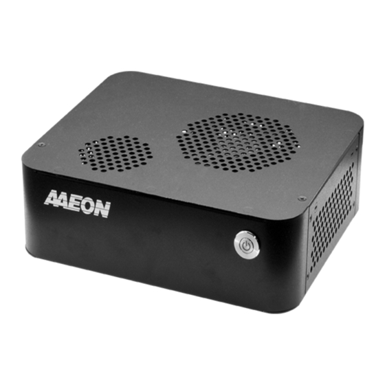
Summary of Contents for Aaeon EPIC-KBS9-PUC
- Page 1 EPIC-KBS9-PUC BOX PC User’s Manual 1 Last Updated: April 2, 2019...
- Page 2 AAEON assumes no liabilities resulting from errors or omissions in this document, or from the use of the information contained herein. AAEON reserves the right to make changes in the product design without notice to its users.
- Page 3 Acknowledgements All other product names or trademarks are properties of their respective owners. The publisher and writer of this document make no claim to ownership of these products, nor is any claim implied for products not specifically named in this section. Microsoft Windows is a registered trademark of Microsoft Corp.
- Page 4 Packing List Before setting up your product, please make sure the following items have been shipped: Item Quantity EPIC-KBS9-PUC If any of these items are missing or damaged, please contact your distributor or sales representative immediately. Preface...
- Page 5 (if any), its specifications, dimensions, jumper/connector settings/definitions, and driver installation instructions (if any), to facilitate users in setting up their product. Users may refer to the product page at AAEON.com for the latest version of this document. Preface...
- Page 6 Safety Precautions Please read the following safety instructions carefully. It is advised that you keep this manual for future references All cautions and warnings on the device should be noted. Make sure the power source matches the power rating of the device. Position the power cord so that people cannot step on it.
- Page 7 If any of the following situations arises, please the contact our service personnel: Damaged power cord or plug Liquid intrusion to the device iii. Exposure to moisture Device is not working as expected or in a manner as described in this manual The device is dropped or damaged Any obvious signs of damage displayed on the device...
- Page 8 FCC Statement This device complies with Part 15 FCC Rules. Operation is subject to the following two conditions: (1) this device may not cause harmful interference, and (2) this device must accept any interference received including interference that may cause undesired operation.
- Page 9 China RoHS Requirements (CN) 产品中有毒有害物质或元素名称及含量 AAEON Main Board/ Daughter Board/ Backplane 有毒有害物质或元素 部件名称 铅 汞 镉 六价铬 多溴联苯 多溴二苯醚 (Pb) (Hg) (Cd) (Cr(VI)) (PBB) (PBDE) 印刷电路板 ○ ○ ○ ○ ○ ○ 及其电子组件 外部信号 ○ ○ ○ ○ ○ ○...
- Page 10 China RoHS Requirement (EN) Poisonous or Hazardous Substances or Elements in Products AAEON Main Board/ Daughter Board/ Backplane Poisonous or Hazardous Substances or Elements Hexavalent Polybrominated Polybrominated Component Lead Mercury Cadmium Chromium Biphenyls Diphenyl Ethers (Pb) (Hg) (Cd) (Cr(VI)) (PBB) (PBDE) PCB &...
-
Page 11: Table Of Contents
Table of Contents Chapter 1 - Product Specifications..................1 Specifications ......................2 Chapter 2 – Hardware Information ..................1 Dimensions ....................... 2 Jumpers and Connectors ..................6 List of Jumpers ......................8 2.3.1 Clear CMOS Jumper (JP6) ................9 2.3.2 AT/ATX mode Selection (JP7) .............. - Page 12 2.4.17 External +12V Input [Reserved] (CN27) ..........23 2.4.18 CRT (CN31) ....................24 2.4.19 PCIE [x4] Slot (CN53) ................24 2.4.20 LAN (RJ-45) Port1~4 (CN54) ..............25 2.4.21 System FAN Connector (CN56) .............. 25 2.4.22 LAN (RJ-45) Port1~2 [Reserved] (CN57)..........26 2.4.23 DDR4 SO-DIMM Slot (DIMM1 &...
- Page 13 3.7.1 BBS Priorities ....................22 Setup Submenu: Save & Exit ................23 Chapter 4 – Driver Installation ....................1 Driver Installation ..................... 2 Appendix A – Mating Connectors ..................4 List of Mating Connectors and Cables ..............5 Appendix B - I/O Information ....................6 I/O Address Map .....................
-
Page 14: Chapter 1 - Product Specifications
Chapter 1 Chapter 1 - Product Specifications... -
Page 15: Specifications
Specifications System 4” EPIC Board Form Factor 6th/7th Generation Intel® Core™ i7/i5/i3/Celeron® S-series (Supports 35~65W) H110/H170/Q170 (6W) Chipset DDR4 (Non-ECC) SODIMM x 2, 2133MHz, up Memory Type to 32G Up to 32G Max. Memory Capacity BIOS ... - Page 16 System CE/FCC Class A Certification 1 Grms/ 5~500 Hz/ operation—with mSATA Anti-vibration Display 6th/7th Generation Intel® Core™ VGA/LCD Controller i3/i5/i7/Celeron® HDMI (Rear), VGA (Internal Only) Video Output Backlight Inverter Supply Intel® i211 10/100/1000Base-TX x 2 or 4 ports Ethernet ...
- Page 17 Touch Chapter 1 – Product Specifications...
-
Page 18: Chapter 2 - Hardware Information
Chapter 2 Chapter 2 – Hardware Information... -
Page 19: Dimensions
Dimensions Top and Side Front Chapter 2 – Hardware Information... - Page 20 Rear EPIC-KBS9-PUC-A10-0002 Rear EPIC-KBS9-PUC-A10-0001 Chapter 2 – Hardware Information...
- Page 21 Board Component Side Chapter 2 – Hardware Information...
- Page 22 Board Solder Side Chapter 2 – Hardware Information...
-
Page 23: Jumpers And Connectors
Jumpers and Connectors Component Side Chapter 2 – Hardware Information... - Page 24 Solder Side Chapter 2 – Hardware Information...
-
Page 25: List Of Jumpers
List of Jumpers Please refer to the table below for all of the board’s jumpers that you can configure for your application. Label Function Clear CMOS Jumper AT/ATX Mode Selection Front Panel PIN Header Chapter 2 – Hardware Information... -
Page 26: Clear Cmos Jumper (Jp6)
2.3.1 Clear CMOS Jumper (JP6) Clear CMOS Normal (Default) 2.3.2 AT/ATX mode Selection (JP7) AT mode ATX mode (Default) Chapter 2 – Hardware Information... -
Page 27: Front Panel Pin Header (Jp9)
2.3.3 Front Panel PIN Header (JP9) Pin Name Signal Type Signal Level EXT_PWRBTN# HDD_LED- HDD_LED+ +3.3V SPKR- SPKR+ PWR_LED+ +3.3V HWRST# Chapter 2 – Hardware Information... -
Page 28: List Of Connectors
List of Connectors The table below lists all of the board’s connectors, configurable for your application. Label Function External +12V Input [Default] Audio Port RTC Battery Connector +5V Output for SATA HDD USB 2.0 Port USB 2.0 Port CN10 SATA Port CN11 Mini-Card / mSATA Connector CN13... -
Page 29: External +12V Input (Cn2)
2.4.1 External +12V Input (CN2) Pin Name Signal Type Signal Level +12V +12V 2.4.2 Audio Port (CN5) Pin Name Signal Type Signal Level MIC_L MIC_R LIN_L LIN_R LOUT_L LOUT_R +V5A_AUD Chapter 2 – Hardware Information... -
Page 30: Rtc Battery Connector (Cn6)
2.4.3 RTC Battery Connector (CN6) Pin Name Signal Type Signal Level +3.3V +3.3V 2.4.4 +5V Output for SATA HDD (CN7) Pin Name Signal Type Signal Level +V5S 2.4.5 USB 2.0 Port (CN8) Pin Name Signal Type Signal Level +V5A_USB USB2_D- DIFF USB2_D+ DIFF... -
Page 31: Usb 2.0 Port (Cn9)
2.4.6 USB 2.0 Port (CN9) Pin Name Signal Type Signal Level +V5A_USB USB2_D- DIFF USB2_D+ DIFF 2.4.7 SATA Port (CN10) Pin Name Signal Type Signal Level SATA_TX+ DIFF SATA_TX- DIFF SATA_RX- DIFF SATA_RX+ DIFF Chapter 2 – Hardware Information... -
Page 32: Mini-Card/Msata Connector (Cn11)
2.4.8 Mini-Card/mSATA Connector (CN11) Pin Name Signal Type Signal Level PCIE_WAKE# +3.3VSB/+3.3V +3.3V +1.5V +1.5V PCIE_CLK_REQ# UIM_PRW UIM_DATA PCIE_REF_CLK- DIFF UIM_CLK PCIE_REF_CLK+ DIFF UIM_RST UIM_VPP W_DISABLE# +3.3V Chapter 2 – Hardware Information... - Page 33 Pin Name Signal Type Signal Level PCIE_RST# +3.3V PCIE_RX-/mSATARX+ DIFF +3.3VSB/+3.3V +3.3V PCIE_RX+/mSATARX- DIFF +1.5V +1.5V SMB_CLK +3.3V PCIE_TX-/mSATATX- DIFF SMB_DATA +3.3V PCIE_TX+/mSATATX+ DIFF USB_D- DIFF USB_D+ DIFF +3.3VSB/+3.3V +3.3V +3.3VSB/+3.3V +3.3V Chapter 2 – Hardware Information...
-
Page 34: Sata Port (Cn13)
Pin Name Signal Type Signal Level +1.5V +1.5V +3.3VSB/+3.3V +3.3V 2.4.9 SATA Port (CN13) Pin Name Signal Type Signal Level SATA_TX+ DIFF SATA_TX- DIFF SATA_RX- DIFF SATA_RX+ DIFF Chapter 2 – Hardware Information... -
Page 35: Cpu Fan Connector (Cn14)
2.4.10 CPU FAN Connector (CN14) Pin Name Signal Type Signal Level +V12S/+V5S +12V/+5V TACH ※ +12V/+5V can be set by BOM(R768-+12V/R766-+5V) [Default:+12V] 2.4.11 LPC Port (CN15) Pin Name Signal Type Signal Level LAD0 +3.3V IN/OUT LAD1 IN/OUT +3.3V LAD2 IN/OUT +3.3V LAD3 IN/OUT... -
Page 36: Com Port (Cn16)
2.4.12 COM Port (CN16) Pin Name Signal Type Signal Level ±9V ±9V ±9V RI/+5V/+12V IN/ PWR +5V/+12V ※ COM RS-232/422/485 can be set by BIOS setting. Default is RS-232. ※ COM RI/+5V/+12V function can be set by BOM(R1971-RI/R1972-+12V/R1973-+5V) Chapter 2 – Hardware Information... -
Page 37: Com Port (Cn17)
2.4.13 COM Port (CN17) Pin Name Signal Type Signal Level ±9V ±9V ±9V RI/+5V/+12V IN/ PWR +5V/+12V ※ COM RS-232/422/485 can be set by BIOS setting. Default is RS-232. ※ COM RI/+5V/+12V function can be set by BOM(R1968-RI/R1970-+12V/R1969-+5V) Chapter 2 – Hardware Information... -
Page 38: Usb 2.0/3.0 Port 1~Port 2 (Cn22)
2.4.14 USB 2.0/3.0 Port 1~Port 2 (CN22) Pin Name Signal Type Signal Level +V5SB USB3_D- DIFF USB3_D+ DIFF USB3_SSRX− DIFF USB3_SSRX+ DIFF USB3_SSTX− DIFF USB3_SSTX+ DIFF +V5SB USB4_D- DIFF USB4_D+ DIFF USB4_SSRX− DIFF USB4_SSRX+ DIFF USB4_SSTX− DIFF USB4_SSTX+ DIFF Chapter 2 – Hardware Information... -
Page 39: Hdmi (Cn23)
2.4.15 HDMI (CN23) Pin Name Signal Type Signal Level HDMI_TX2+ DIFF HDMI_TX2- DIFF HDMI_TX1+ DIFF HDMI_TX1- DIFF HDMI_TX0+ DIFF HDMI_TX0- DIFF HDMI_CLK+ DIFF HDMI_CLK- DIFF DDC_CLK DDC_DATA HDMI_HPD Chapter 2 – Hardware Information... -
Page 40: Dio (Cn24)
2.4.16 DIO (CN24) Pin Name Signal Type Signal Level DIO0 DIO1 DIO2 DIO3 DIO4 DIO5 DIO6 DIO7 +V5S 2.4.17 External +12V Input [Reserved] (CN27) Pin Name Signal Type Signal Level +12V +12V +12V +12V Chapter 2 – Hardware Information... -
Page 41: Crt (Cn31)
2.4.18 CRT (CN31) Pin Name Signal Type Signal Level GREEN BLUE +V5S_DISP_CON DATA 2.4.19 PCIE [x4] Slot (CN53) Standard specification Chapter 2 – Hardware Information... -
Page 42: Lan (Rj-45) Port1~4 (Cn54)
2.4.20 LAN (RJ-45) Port1~4 (CN54) Pin Name Signal Type Signal Level MDI0+ DIFF MDI0- DIFF MDI1+ DIFF MDI2+ DIFF MDI2- DIFF MDI1- DIFF MDI3+ DIFF MDI3- DIFF 2.4.21 System FAN Connector (CN56) Pin Name Signal Type Signal Level +V12S/+V5S +12V/+5V TACH ※... -
Page 43: Lan (Rj-45) Port1~2 [Reserved] (Cn57)
2.4.22 LAN (RJ-45) Port1~2 [Reserved] (CN57) Pin Name Signal Type Signal Level MDI0+ DIFF MDI0- DIFF MDI1+ DIFF MDI2+ DIFF MDI2- DIFF MDI1- DIFF MDI3+ DIFF MDI3- DIFF 2.4.23 DDR4 SO-DIMM Slot (DIMM1 & DIMM2) Standard specification Chapter 2 – Hardware Information... -
Page 44: Block Diagram
Block Diagram Chapter 2 – Hardware Information... -
Page 45: Chapter 3 - Bios Setup
Chapter 3 Chapter 3 - BIOS Setup... -
Page 46: System Test And Initialization
System Test and Initialization The EPIC-KBS9-PUC board uses certain routines to test and initialize board hardware. If the routines encounter an error during the tests, you will either hear a few short beeps or see an error message on the screen. There are two kinds of errors: fatal and non-fatal. -
Page 47: Ami Bios Setup
AMI BIOS Setup AMI BIOS ROM has a built-in Setup program that allows users to modify the basic system configuration. This information is stored in a battery-backed CMOS RAM and BIOS NVRAM so that it retains the Setup information when the power is turned off. To enter setup, power on the computer and press <Del>or <ESC>... -
Page 48: Setup Submenu: Main
Setup Submenu: Main Date and Time can be set here. Press <Tab> to switch between elements. Chapter 3 – BIOS Setup... -
Page 49: Setup Submenu: Advanced
Setup Submenu: Advanced Chapter 3 – BIOS Setup... -
Page 50: Cpu Configuration
3.4.1 CPU Configuration Options Summary Intel (VMX) Disabled Virtualization Enabled Optimal Default, Failsafe Default Technology When enabled, a VMM can utilize the additional hardware capabilities provided by Vanderpool Technology. C states Disabled Enabled Optimal Default, Failsafe Default Enabled for Windows XP and Linux (OS optimized for Hyper-Threading Technology) and Disable for other OS (OS not optimized for Hyper-Threading Technology). -
Page 51: Trusted Computing
3.4.2 Trusted Computing Options Summary Security Device Enabled Optimal Default, Failsafe Default Support Disabled Enable/Disable Security Device. NOTE: Your Computer will reboot during restart in order to change State of the Device. Chapter 3 – BIOS Setup... -
Page 52: Sata Configuration
3.4.3 SATA Configuration Options Summary SATA Controller(s) Enabled Optimal Default, Failsafe Default Disabled Enable or disable SATA Device. SATA Mode AHCI Mode Optimal Default, Failsafe Default RAID Mode Determines how SATA controller(s) operate. Port 0 Disabled Enabled Optimal Default, Failsafe Default Enable or Disable SATA Port. -
Page 53: Usb Configuration
3.4.4 USB Configuration Options Summary Legacy USB Support Enabled Optimal Default, Failsafe Default Disabled Auto Enables BIOS Support for Legacy USB Support. When enabled, USB can be functional in legacy environment like DOS. AUTO option disables legacy support if no USB devices are connected Device Name (Emulation Auto Optimal Default, Failsafe Default... -
Page 54: Hardware Monitor
3.4.5 Hardware Monitor Chapter 3 – BIOS Setup... -
Page 55: Smart Fan Mode Configuration
3.4.5.1 Smart Fan Mode Configuration Smart Fan Mode Configuration Menu – Auto Duty Cycle Mode Selected Options Summary Fan1 Smart Fan Manual Duty Mode control Auto Duty-Cycle Mode Optimal Default, Failsafe Default Fan2 Smart Fan Manual Duty Mode control Auto Duty-Cycle Mode Optimal Default, Failsafe Default Chapter 3 –... - Page 56 Smart Fan Mode Configuration Menu – Manual Duty Mode Selected Options Summary Manual Setting Optimal Default, Failsafe Default Set Fan at fixed Duty-Cycle Min=0 Max=100 Please input Dec number: Chapter 3 – BIOS Setup...
-
Page 57: Sio Configuration
3.4.6 SIO Configuration Chapter 3 – BIOS Setup... -
Page 58: Serial Port Configuration
3.4.6.1 Serial Port Configuration Options Summary Use This Device Disabled Enabled Optimal Default, Failsafe Default Enable/Disable Serial Port (COM) Possible: Use Automatic Settings Optimal Default, Failsafe Default IO=2F8; IRQ=3; IO=3F8; IRQ=4; Select an optimal setting for IO device Mode RS232 Optimal Default, Failsafe Default RS422 RS485... -
Page 59: Power Management
3.4.7 Power Management Options Summary Power Mode ATX Type Optimal Default, Failsafe Default AT Type Select power supply mode. Restore AC Power Last State Optimal Default, Failsafe Default LOSS Power On Power Off Select power state when power is re-applied after a power failure. RTC wake system Disabled Optimal Default, Failsafe Default... -
Page 60: Setup Submenu: Chipset
Setup Submenu: Chipset Chapter 3 – BIOS Setup... -
Page 61: System Agent (Sa) Configuration
3.5.1 System Agent (SA) Configuration Options Summary Max TOLUD Dynamic Optimal Default, Failsafe Default 1 GB 1.25 GB 1.5 GB 1.75 GB 2 GB 2.25 GB 2.5 GB 2.75 GB 3 GB 3.25 GB Maximum Value of TOLUD Dynamic assignment will adjust TOLUD automatically based on largest MMIO length of installed graphic controller. -
Page 62: Graphics Configuration
3.5.1.1 Graphics Configuration Options Summary Primary IGFX Boot VBIOS Default Optimal Default, Failsafe Default Display HDMI Select the Video Device which will be activated during POST. This has no effect if external graphic present. Secondary boot display selection will appear based on your selection. Internal Graphics AUTO Optimal Default, Failsafe Default... -
Page 63: Pch-Io Configuration
3.5.2 PCH-IO Configuration Options Summary PCIE/mSATA Switch PCIE SATA Optimal Default, Failsafe Default Select function enabled for Half-MiniCard(CN13) slot Me FW Image Disabled Re-Flash Enabled Optimal Default, Failsafe Default Auto Enable/Disable Me FW Image Re-Flash function. Chapter 3 – BIOS Setup... -
Page 64: Setup Submenu: Security
Setup Submenu: Security Set User/Supervisor Password You can set an Administrator Password in this menu. If an Administrator Password is set, you will be able to then set a User Password. User Password limits access to many of the features in the Setup utility. To set a password, select the password you want to set and then press <Enter>. -
Page 65: Setup Submenu: Boot
Setup Submenu: Boot Options Summary Setup Prompt Timeout Optimal Default, Failsafe Default Number of seconds to wait for setup activation key. 65535(0xFFFF) means indefinite waiting. Bootup NumLock State Optimal Default, Failsafe Default Select the keyboard NumLock state Quiet Boot Disabled Enabled Optimal Default, Failsafe Default Enable/Disable showing boot logo. -
Page 66: Bbs Priorities
Options Summary Boot mode select LEGACY Optimal Default, Failsafe Default UEFI DUAL Select boot mode LEGACY/UEFI 3.7.1 BBS Priorities Chapter 3 – BIOS Setup... -
Page 67: Setup Submenu: Save & Exit
Setup Submenu: Save & Exit Chapter 3 – BIOS Setup... - Page 68 Chapter 4 Chapter 4 – Driver Installation...
-
Page 69: Chapter 4 - Driver Installation
Driver Installation Drivers for the EPIC-KBS9-PUC can be downloaded from the product page on the AAEON website by following this link: https://www.aaeon.com/en/p/epic-boards-epic-kbs9-puc Download the driver(s) you need and follow the steps below to install them. Step 1 – Install Chipset Drivers Open the Step 1 –... - Page 70 Step 4 – Install Serial Port Drivers Open the Step 4 – Serial Port Driver (Optional) folder and select your SKU and OS Open the FintekSerial.exe file in the folder Follow the instructions Drivers will be installed automatically Chapter 4 – Driver Installation...
-
Page 71: Appendix A - Mating Connectors
Appendix A Appendix A – Mating Connectors... -
Page 72: List Of Mating Connectors And Cables
887505318 SATA Cable 1709070500 CN13 SATA Port Molex 887505318 SATA Cable 1709070500 CPU FAN CN14 Molex 47054-1000 17592KBS90 Connector AAEON LPC CN15 LPC Connector SHR-12V-S-B 1703120130 Cable CN16 COM Port Molex 51021-0900 COM Cable 1701090150 CN17 COM Port Molex 51021-0900... -
Page 73: Appendix B - I/O Information
Appendix B Appendix B - I/O Information... -
Page 74: I/O Address Map
I/O Address Map Appendix A – Mating Connectors... - Page 75 Appendix A – Mating Connectors...
-
Page 76: Memory Address Map
Memory Address Map Appendix A – Mating Connectors... - Page 77 Appendix A – Mating Connectors...
-
Page 78: Irq Mapping Chart
IRQ Mapping Chart Appendix A – Mating Connectors... - Page 79 Appendix A – Mating Connectors...
-
Page 80: Appendix C - Digital I/O Ports
Appendix C Appendix C – Digital I/O Ports... -
Page 81: Digital I/O Register
Digital I/O Register Appendix C – Digital I/O Ports... - Page 82 Appendix C – Digital I/O Ports...
- Page 83 Appendix C – Digital I/O Ports...
-
Page 84: Digital I/O Sample Code
Digital I/O Sample Code UINT32 SOC_GPIO_BASE_ADDRESS=0xFDAE06A8,SOC_GPIO_VAL=0; (i = 0; i < 8; i++) SOC_GPIO_VAL=MmioRead32(SOC_GPIO_BASE_ADDRESS+8*i); (SetupData.SOCGPPGx_Oe[i]==0)//GPIO set to input SOC_GPIO_VAL |= BIT8;//Set bit 8 SOC_GPIO_VAL &= (~BIT9);//Clear bit 9 else if (SetupData.SOCGPPGx_Oe[i]==1)//GPIO set to output SOC_GPIO_VAL |= BIT9;//Set bit 9 SOC_GPIO_VAL &= (~BIT8);//Clear bit 8 if(SetupData.SOCGPPGx_Val[i]==0) SOC_GPIO_VAL &=... -
Page 85: Appendix D - Watchdog Timer Programming
Appendix D Appendix D - Watchdog Timer Programming... -
Page 86: Watchdog Timer Registers
Watchdog Timer Registers Table 1 : Watch dog relative IO address Default Value Note I/O Base I/O Base address for Watchdog operation. 0xA10 Address This address is assigned by SIO LDN7, register 0x60-0x61. Table 2 : Watchdog relative register table Register Offset BitNum... -
Page 87: Watchdog Sample Program
Watchdog Sample Program ****************************************************************************** // WDT I/O operation relative definition (Please reference to Table 1) #define WDTAddr 0x510 // WDT I/O base address Void WDTWriteByte(byte Register, byte Value); byte WDTReadByte(byte Register); Void WDTSetReg(byte Register, byte Bit, byte Val); // Watch Dog relative definition (Please reference to Table 2) #define DevReg 0x00 // Device configuration register #define WDTRstBit 0x80 // Watchdog WDTRST# (Bit7) - Page 88 VOID AaeonWDTEnable (){ WDTEnableDisable(1); // Procedure : AaeonWDTConfig VOID AaeonWDTConfig (byte Counter, BOOLEAN Unit){ // Disable WDT counting WDTEnableDisable(0); // Clear Watchdog Timeout Status WDTClearTimeoutStatus(); // WDT relative parameter setting WDTParameterSetting(Timer, Unit); VOID WDTEnableDisable(byte Value){ If (Value == 1) WDTSetBit(TimerReg, EnableBit, 1); else WDTSetBit(TimerReg, EnableBit, 0);...
- Page 89 VOID WDTWriteByte(byte Register, byte Value){ IOWriteByte(WDTAddr+Register, Value); byte WDTReadByte(byte Register){ return IOReadByte(WDTAddr+Register); VOID WDTSetBit(byte Register, byte Bit, byte Val){ byte TmpValue; TmpValue = WDTReadByte(Register); TmpValue &= ~(1 << Bit); TmpValue |= Val << Bit; WDTWriteByte(Register, TmpValue); ******************************************************************************* Appendix A – Watchdog Timer Programming...
Need help?
Do you have a question about the EPIC-KBS9-PUC and is the answer not in the manual?
Questions and answers