
Related Manuals for Aeroflex 3035


Summary of Contents for Aeroflex 3035
- Page 1 3035 Wideband RF Digitizer PXI Module Operating Manual Document no. 46892/722 Issue 8 20 October 2008...
-
Page 2: About This Manual
This manual applies when the instrument is used with the supplied software. It explains how to set up and configure an Aeroflex 3035 wideband RF digitizer PXI module. Where necessary, it refers you to the appropriate installation documents that are supplied with the module. -
Page 3: Intended Audience
PREFACE Intended audience Users who need to configure and operate the 3035 wideband RF digitizer to down-convert and digitize RF signals. This manual is intended for first-time users, to provide familiarity with basic operation. Programming is not covered in this document but is documented fully in the... - Page 4 PREFACE Checking the software compatibility of a PXI module • Modules that are compatible with all driver versions display on their front panel a serial number label consisting of black lettering on a white background. • Modules that are only compatible with software driver installation version 6.2.0 and higher have a serial number label consisting of black lettering on a yellow background.
-
Page 5: Associated Documentation
PREFACE Associated documentation The following documentation covers specific aspects of this equipment: Part no. Compilation containing soft front panels, drivers, PXI Modules CD-ROM 46886/028 application software, data sheets, getting started and operating manuals for this and other modules in the 3000 Series. Part no. -
Page 6: The Pxi Concept
VXI timing and triggering, and VXIplug&play instrument drivers to provide powerful and affordable systems. ® is a registered trademark of Aeroflex International Inc. in the US PXI™ is a registered trademark of the PXI Systems Alliance Windows™, Windows XP™ and Windows NT™ are trademarks of Microsoft Corporation... - Page 7 PREFACE Abbreviations/acronyms ACLR Adjacent Channel Leakage Ratio Adjacent Channel Power ACPR Adjacent Channel Power Ratio Analog-to-Digital Converter Amplitude Modulation Arbitrary Waveform Generator Continuous Wave Digital-to-Analog Converter Decibels Decibels relative to the carrier level Decibels relative to 1 mW Fast Fourier Transform Frequency Modulation FPGA Field Programmable Gate Array...
- Page 8 PREFACE PCI eXtensions for Instrumentation Radio Frequency Root Mean Square Soft Front Panel SubMiniature version A (connector) SubMiniature version B (connector) TDMA Time Division Multiple Access TRIG Trigger Transistor-Transistor Logic Unit Under Test Voltage-Controlled Oscillator VHDCI Very High Density Connector Interface VSWR Voltage Standing-Wave Ratio VMEbus Extension for Instrumentation...
-
Page 9: Chapter 1 General Information
Welcome to the operating manual for the 3035 Wideband RF Digitizer PXI module. The 3035, when used with a 3010 Series PXI RF synthesizer module, forms a compact wideband RF digitizer that occupies three slots in a 3U PXI chassis. - Page 10 LVDS port. Software supplied with the module allows for spectrum analysis of the digitized signals. The 3035 can be used in RF test and measurement systems used in development or manufacturing. Applications span all areas of UHF radio communications.
- Page 11 An instrument-level soft front panel is also provided, together with a dll and COM object, combining the controls of the 3035 together with the 3010 Series RF synthesizer. Refer to Getting Started with afDigitizer (part no. 46892/676) supplied on the PXI Modules CD-ROM part no.
-
Page 12: Deliverable Items
GENERAL INFORMATION Deliverable items • 3035 Wideband RF Digitizer PXI module • PXI Modules CD-ROM (part no. 46886/028), containing soft front panels, drivers, application software, data sheets, getting started and operating manuals for this and other modules in the 3000 Series •... -
Page 13: Chapter 2 Installation
Chapter 2 INSTALLATION WARNING Initial visual inspection Refer to the 3000 Series Common Installation Guide 46882/663. Handling precautions Refer to the 3000 Series Common Installation Guide 46882/663. Hardware installation Installing the module into the PXI chassis Refer to the 3000 Series Common Installation Guide 46882/663 and Installation Guide for Chassis 46882/667. -
Page 14: Connector Care And Maintenance
INSTALLATION Connector care and maintenance How to connect and torque an SMA connector 1 First, ensure that the mating halves of the connector are correctly aligned. 2 Next, engage the threads of the nut and tighten it by hand, ensuring that the mating halves do not move relative to each other. -
Page 15: Front Panel Connectors
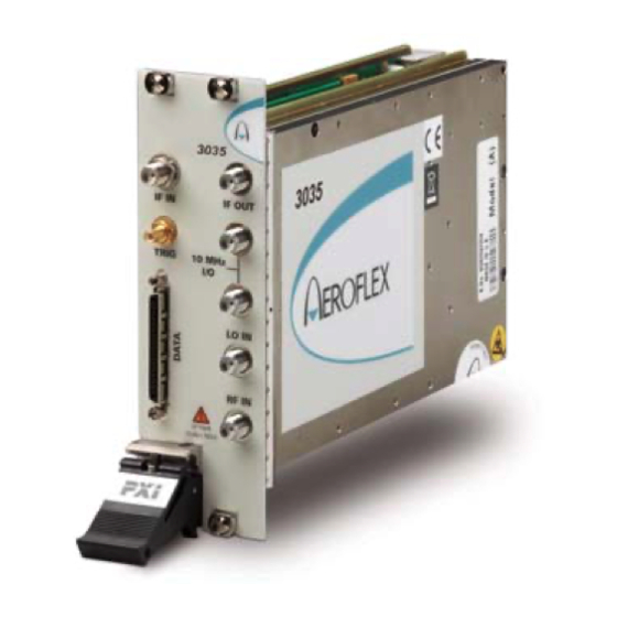
77.76 MHz input, −15 to +10 dBm for full- IF IN scale digitizer. SMA socket, 50 Ω. C5990 Maximum safe powers Fig. 3-1 3035 front panel RF input: +30 dBm continuous (minimum 0 dB input attenuation, 10 dB IF attenuation) IF input: +10 dBm (0 dB IF attenuation) -
Page 16: Detailed Help Information
Open the AF3030_sfp.exe file: this is in the C:\VXIPNP|WinNT\af3030\ directory on a Windows NT machine, for example. It is also accessible from the Windows Start menu under Programs\Aeroflex\PXI Module Front Panels\AF3030 Front Panel. The soft front panel, similar to that in Fig. 3-2, is displayed. - Page 17 OPERATION IF/IQ data format Menu bar Input source Boot C6190 Acquisition & RF tuning Input conditioning triggering Fig. 3-2 3035 soft front panel...
- Page 18 Soft front panel controls Menu bar File Save Captured Data (as ASCII file)… captures the 16-bit sample data into the specified ASCII file. Save Captured Data (as Binary file)… captures the 16-bit sample data into the specified binary file. Click Exit to close the application. Settings Load and Save allow you to load and save soft front panel configurations from and to your preferred locations.
- Page 19 MENU BAR ON SOFT FRONT PANEL LVDS allows you to set each LVDS Data, Auxiliary and Marker mode for input, output or tri-state (default) operation. Spare 0 is controlled by LVDS Data Mode. To use Spare 0 as a trigger input, set •...
- Page 20 PXI backplane bus, the DATA connector and the TRIG input, as shown diagrammatically in Fig. 3-3. This provides great flexibility in how you can route signals between modules. PXI_STAR PXI_LBL[0]–[12] PXI_TRIG[0]–[7] PXI BACKPLANE BUS ROUTING MATRIX TRIG 3035 PXI MODULE C5991 DATA LVDS_MARKER1–4 LVDS_AUX[0]–[4] LVDS_SPARE[0]–[2] Fig. 3-3 Routing matrix in 3035...
- Page 21 Load and Save commands in Settings, or use Routing Scenarios to access pre-set alternative routings, or contact Aeroflex if you need assistance in defining particular routing requirements.
- Page 22 MENU BAR ON SOFT FRONT PANEL Output enable Input signal check boxes selection C6193 Output signals Input signals Fig. 3-4 Routing matrix inputs and outputs...
- Page 23 MENU BAR ON SOFT FRONT PANEL Optimization allows you to choose how the module compensates for the effect of temperature changes and RF frequency response. Auto Temperature Optimization (default) monitors the temperature of the module at regular intervals and adjusts the correction figure for the current temperature. You can turn this off if it might interfere with a time-critical measurement.
- Page 24 MENU BAR ON SOFT FRONT PANEL Options Allows you to enable or disable additional instrument options if you have the appropriate password (available from the Aeroflex sales desk). Click Edit… to display the options screen (Fig. 3-5). Fig. 3-5 Options screen Disabled options are shown grayed out.
- Page 25 MENU BAR ON SOFT FRONT PANEL View Allows you to view results in different formats. View FFT (default) displays a single graph showing logarithmic power versus frequency. The default span is 66% of full span. You can modify the top of screen reference power (dBm) and the vertical scaling (dB/div).
-
Page 26: Fft Display
MENU BAR ON SOFT FRONT PANEL FFT Display This menu is enabled only when View\View FFT is selected. It allows you to hide/display the graticule and save the dB levels of the trace as a .txt or other file. Graticule Visible hides or displays the graticule. The Span menu selects either Full or Truncated (approx. - Page 27 MENU BAR ON SOFT FRONT PANEL Time Series Display When View Time Series is selected, the Time Series Display menu is enabled, allowing you view I and Q traces on two separate graphs or overlaid in different colors. Graticule Visible hides or displays the graticule. IQ Separate Graphs displays separate graphs of Time Series (I) and Time Series (Q).
- Page 28 MENU BAR ON SOFT FRONT PANEL Capture By default, the module captures data to the screen (To Screen Only), but you can also capture results to ASCII or binary files whilst continuing to display on screen (To ASCII File and Screen; To Binary File and Screen). File Setup…...
- Page 29 Click Boot to initialize the module and view the Boot Resource window. Resources available for initializing are shown in blue. Select the 3035 you want to boot. Boot default FPGA configuration box. Check this. Do not change the configuration unless you are advised otherwise.
-
Page 30: Input Source
Input source Set this to RF or IF depending on which input is used (IF IN or RF IN). Apply IF or RF signals to the appropriate input connector. If the signal is RF, the module downconverts it and provides attenuator configuration and filtering options (see Input conditioning). - Page 31 Shows the frequency to which a 3010 Series RF synthesizer module or other source should be set in order to provide the correct LO frequency for the 3035. If you are using a 3010 Series module, simply double-click on the field, copy the value, and paste it into the RF Frequency (Hz) field on the 3010 Series module’s soft front panel.
-
Page 32: External Reference
RF TUNING ON SOFT FRONT PANEL External Reference Lock to 10MHz causes the ADC clock to lock to the 10 MHz reference connected to the 10 MHz I/O connector. Free Run causes the ADC clock to free run at the center of its range, at a nominal frequency of 103.68 MHz. -
Page 33: Input Conditioning
Input conditioning You may find the block schematic diagram (Fig. 4-1) helpful in understanding these features. RF Input Level (dBm) Set this to the peak level of the input RF signal to insure the best dynamic range and signal-to- noise ratio. Grayed out when Input Source is set to IF. Set the RF input level using the up/down arrows or by entering the level, in the range −99.99 to +30.00 dBm in Auto Atten Config mode. -
Page 34: Filter Bypass
INPUT CONDITIONING ON SOFT FRONT PANEL IF Atten Sets the IF attenuator value, which changes the input level to the ADC. This value can only be adjusted manually if Atten Config is set to Manual. Set the IF attenuator level using the up/down arrows or by entering the level, in the range 0 to +35 dB in 1 dB steps. - Page 35 INPUT CONDITIONING ON SOFT FRONT PANEL ADC Overload Level Indicates the RF/IF input level that could cause ADC Overload error. The displayed overload level is clamped to the safe input level. Remove DC Offset Removes the DC component from captured IF or IQ data. Removes DC components at the edge of the span at full and/or ½...
- Page 36 Acquisition & triggering Capture Trigger Allows you to select the trigger source from a drop-down list: Software trigger • SW_TRIG This is a non-triggered capture mode. Click on Start to capture samples (defined by Number of Samples) when in Single/Repeat mode, without waiting for any external event.
- Page 37 ACQUISITION AND TRIGGERING ON SOFT FRONT PANEL Most of the hardware triggers share a common triggering interface: Trigger Type Set to Edge or Gate Edge/Gate Polarity Set +ve or –ve Trigger Offset Delay Delays the trigger by a specified number of output sample periods.
- Page 38 ACQUISITION AND TRIGGERING ON SOFT FRONT PANEL Pre-Trig Samples Sets the number of pre-trigger samples present in the captured (Edge trigger type) data buffer. Increase this value to move the position of the trigger point in the captured data further from the start. Samples C5976 Pre-trigger samples...
- Page 39 PXI_LBL (Local Bus Left) [0–12] • Takes its trigger input from the slot to the left of the 3035 (viewed from the front panel), using the PXI local bus. Choose from any of 13 bits for the trigger; this bus is common only to the 3035 and the module to its left.
- Page 40 ACQUISITION AND TRIGGERING ON SOFT FRONT PANEL • INT_TIMER Takes its trigger from the internal timer. This timer trigger can also be routed to other modules using the routing matrix. Similarly, this timer can be synchronized with the external signal connected to the TIMER_SYNC signal in the routing matrix. Click Timer Settings…...
- Page 41 ACQUISITION AND TRIGGERING ON SOFT FRONT PANEL Fig. 3-6 Timer settings Channel Timer when checked, lets you use a different timer period for each Mode channel. The timer period is determined by the active channel’s Period (see below), and applies while that channel is active. This mode is useful in setting up variable dwell list mode.
- Page 42 ACQUISITION AND TRIGGERING ON SOFT FRONT PANEL Period Sets the period of the active channel (in number of output samples) if Channel Timer Mode is enabled. Otherwise, sets the common timer period in μs. Mark/space ratio in either mode is 50%.
- Page 43 ACQUISITION AND TRIGGERING ON SOFT FRONT PANEL • INT_TRIG Takes its trigger from the internal level trigger. 3-29...
- Page 44 ACQUISITION AND TRIGGERING ON SOFT FRONT PANEL Int Trigger Mode Select the internal level trigger mode: Absolute/Relative Absolute: the digitized signal is filtered using an absolute time constant. An internal level trigger is generated when the level of this filtered signal exceeds the absolute level trigger threshold (specified in dBm).
- Page 45 ACQUISITION AND TRIGGERING ON SOFT FRONT PANEL Signal envelope Envelope output, fast time constant filter Envelope output, slow time constant filter +ve trigger point Difference pulse Relative threshold level Internal trigger C6172 Fig. 3-7 Relative internal level trigger mode Trigger mode and control Mode: Selects Single-shot or Repeat data capture.
- Page 46 IF/IQ data format Sample Data Type Select IQ or IF sample data type. IQ Sample Data: output sample rate is determined by the Modulation Mode and • Decimation Ratio IF Sample Data: output sample rate is fixed at 103.68 MHz •...
-
Page 47: Modulation Mode
IQ/IF DATA FORMAT ON SOFT FRONT PANEL Modulation Mode (IQ data format only) Sets the digital modulation mode. Select from Generic, UMTS, GSM, CDMA2000 1X or 2319 Emulation. The sample rate varies, depending upon modulation mode and decimation ratio: Generic: user-defined. Use this mode to create or emulate any modulation scheme. •... - Page 48 IQ/IF DATA FORMAT ON SOFT FRONT PANEL Pre-defined rates: UMTS data mode: 61.44 MHz/2 (where N = 1 to 10) • (4-N) GSM resampled IQ data mode: 13 MHz/(3 * 2 ), where N = 0 to 4 (2 times symbol •...
- Page 49 IQ/IF DATA FORMAT ON SOFT FRONT PANEL IQ Data Output Format Select 16- or 32-bit, subject to the modulation mode and decimation ratio chosen. Sample rates Modulation Decimation ratio IQ sample rate IQ data format (Msymbol/s) GENERIC variable 16 (when Output Sample Rate > 12.96 MHz ) where n = 0 16/32 (when Output Sample Rate <= 12.96 MHz) to 14 (max)
-
Page 50: Window Function
IQ/IF DATA FORMAT ON SOFT FRONT PANEL Window Function Defines the window used by the FFT. 5-term Aeroflex gives good noise performance and side-lobe suppression at the expense of a wider main lobe, optimal for ACPR measurements. Decimated Samp Rate (MHz) Displays the result of the undecimated sampling rate divided by the decimation ratio. - Page 51 List mode operation Introduction List mode operation associates a list address with a particular RF setup (channels 0–127). When the module is set to list mode operation, a new address, when strobed in, causes the module to change to the RF setup (channel) associated with that address. List mode operation facilitates fast channel hopping during, for example, testing of transmitter/receiver modules where numerous different RF level and frequency settings are needed.
- Page 52 LIST MODE Channel List Click Chan List on the soft front panel to display individual channel list settings (Fig. 3-8). This is where you define channel setup for list mode operation. Fig. 3-8 Edit channel list settings 3-38...
- Page 53 LIST MODE Edit individual channel parameters by selecting the specific channel. Channel parameters are: Freq (Hz) LO Position Atten Config RF Level (dBm) IF Level (dBm) RF Atten (dB) IF Atten (dB) Period (μs/output samples Select the channel to be edited either by changing the channel number on the panel or by clicking on the corresponding channel row in the channel list.
- Page 54 LIST MODE Click Timer… to display the Timer Settings screen. Click Edit Range to display the Edit Channel Range screen (Fig. 3-9), which lets you apply changes to a set of channels simultaneously, speeding up channel setup. Define start and finish values for address numbers in the Chan range, from: and to: fields. Insert values and click Set for each field.
-
Page 55: List Mode Settings
LIST MODE Click List Mode to display the List Mode Settings screen, which lets you set up addressing and strobing, and the internal counter. List Mode Settings Click List Mode on the Channel List screen to display the List Mode Settings screen. From here, you can define the list address source, and how the strobe (internal or external) that actions a new list address is handled. -
Page 56: Strobe Polarity
LIST MODE Address Source Defines the source from which the seven-bit-wide list address is obtained. Manual: RF list addresses are register-driven values, manually controlled by setting the RF Channel. External: RF list addresses are sourced from the signal routing matrix (Fig. - Page 57 LIST MODE Counter Stop Defines the stop address of the list counter. If this value is greater than the value of Counter Start, the counter increments; otherwise it decrements. Setting this value also resets the list count to the next start address. Timer Dwell Defines the period of the list timer, in units of 0.1 μs.
-
Page 58: Driver Export Functions
Driver export functions On-line help and functional documentation for driver export functions are available on the CD-ROM supplied with your module. They are installed onto your computer at the same time as the drivers. Driver installation folder Find help and functional documentation in the driver installation folder on your computer. This is typically: C:\vxipnp\winnt\af3030 Help... - Page 59 DRIVER EXPORT FUNCTIONS The file opens at the Contents page: Fig. 3-11 Online help contents — example Hyperlinks from here take you to Introduction Assumptions Error codes Functions listings 3-45...
- Page 60 DRIVER EXPORT FUNCTIONS Functions listings Functions are grouped by type. Click on the hyperlink for details of the function. Each function has a description of its purpose, and may have a list of parameters and return values. Fig. 3-12 Function description — example 3-46...
- Page 61 46892/809), supplied on the CD-ROM with the module, for detailed information on creating a fully functional RF digitizer using the 3035 and 3010/3011 together. The afDigitizer dlls and PXI Studio application combine the functions of the individual modules to provide a single...
- Page 62 Appendix A DATA connector and timing The DATA connector is a 68-way female VHDCI-type LVDS (low-voltage differential signaling) interface. It can be used to output data and associated control and timing signals. The DATA connector is shown in Fig. A-1. LVDS data conforms to ANSI/TIA/EIA-644. C5504 Fig.
- Page 63 DATA CONNECTOR AND TIMING Table A-1 DATA pin-out Contact Function Contact Function AUX0- AUX0+ AUX1+ AUX1− AUX2+ AUX2− SPARE1+ SPARE1− SPARE2+ SPARE2− CLK_IN+ CLK_IN− CLK_OUT+ CLK_OUT− D0− D1− D2− D3− D4− D5− D6− D7− D8− D9− D10+ D10− D11+ D11− D12+ D12−...
-
Page 64: Data Format
DATA CONNECTOR AND TIMING Data format The data output to the DATA interface is real-time. In resample mode, data is output using a 103.68 MHz clock (but bursted to achieve the correct average sample rate). D0-D15 (Sample Sample Data Output Format: DATA) in Output 16-bit IQ: 2 x D[15:0], I followed by Q, D[0]=LSB. -
Page 65: Data Timing
DATA CONNECTOR AND TIMING Data timing Data transmission for generic modulation mode In this mode, IQ data is resampled to produce IQ data in the range 51.84 MHz/2 where N = 0 to 13. Example timing relationships between data rate and clock frequency for the DATA interface are shown in Fig. - Page 66 DATA CONNECTOR AND TIMING Latency The digitizer converts an analog RF waveform presented at its RF port into a series of digital IQ data pairs at its LVDS port. LVDS latency is the time taken for any given point on the input RF waveform to appear as an IQ data pair on the LVDS output.
- Page 67 DATA CONNECTOR AND TIMING Data timing for UMTS modulation mode and decimation ratio of 2 The ADC in the module is clocked at a rate of 103.68 Ms/s. The module’s soft front panel allows both the modulation mode and the decimation ratio to be selected. IQSELECT_OUT is toggled only when an IQ data pair is being transmitted.
- Page 68 DATA CONNECTOR AND TIMING Latency The digitizer converts an analog RF waveform presented at its RF port into a series of digital IQ data pairs at its LVDS port. LVDS latency is the time taken for any given point on the input RF waveform to appear as an IQ data pair on the LVDS output.
- Page 69 DATA CONNECTOR AND TIMING Data timing for UMTS modulation mode and decimation ratio of 4 The timing relationships for the DATA interface are as shown in Fig. A-5. The CLK_OUT signal is continuous and remains fixed at 103.68 MHz, irrespective of the modulation mode and the decimation rate.
- Page 70 DATA CONNECTOR AND TIMING Data timing for UMTS modulation mode and decimation ratio of 8 The timing relationships for the DATA interface are as shown in Fig. A-6. The CLK_OUT signal is continuous and remains fixed at 103.68 MHz, irrespective of the modulation mode and the decimation rate.
- Page 71 DATA CONNECTOR AND TIMING Data timing for CDMA2000 1X modulation mode If a modulation mode of CDMA2000 1X and a decimation value of 1 are both selected, IQ data is generated at eight times the CDMA2000 1X chip rate. As the chip rate is 1.2288 MHz, this gives an IQ sample rate of 9.8304 Ms/s.
- Page 72 DATA CONNECTOR AND TIMING Latency The digitizer converts an analog RF waveform presented at its RF port into a series of digital IQ data pairs at its LVDS port. LVDS latency is the time taken for any given point on the input RF waveform to appear as an IQ data pair on the LVDS output.
- Page 73 DATA CONNECTOR AND TIMING Data transmission for GSM modulation mode and a decimation ratio of 1 In this mode the IQ data is resampled to produce IQ data at 16 times the GSM symbol rate of 270.83 kHz, that is, 4.333 Ms/s. The timing relationships for the DATA interface is as shown in Fig.
- Page 74 DATA CONNECTOR AND TIMING Data transmission for 2319E emulation mode In this mode, the IQ data is resampled to produce IQ data at 4.08 MHz with a decimation ratio of 16. The timing relationships for the DATA interface are as shown in Fig. A-10. Note that the CLK_OUT signal is continuous and that the frequency of the clock remains fixed at 103.68 MHz.
- Page 75 DATA CONNECTOR AND TIMING Data transmission in IF data format In IF data format, the IQ_SELECT signal remains low and IF data is clocked on each ADC clock cycle at a fixed sample rate of 103.68 MHz Latency LVDS latency in IF data format is the time taken for any given point on the input RF waveform to appear as IF data on the LVDS output.
-
Page 76: Chapter 4 Brief Technical Description
Chapter 4 BRIEF TECHNICAL DESCRIPTION Introduction 3035 is a PXI RF bandpass digitizer, digitizing an instantaneous IF bandwidth of 36 MHz with a 14-bit converter. Digitized RF can be stored in a large internal RAM and read back over the PXI bus. It can also be streamed out of a front panel LVDS output at full speed. - Page 77 BRIEF TECHNICAL DESCRIPTION The RF synthesizer generates a top octave of 1500 MHz to 3 GHz. This is applied to the LO input, which is amplified to provide level control, then split between the through path and the dividers. It is divided down for frequencies below 1500 MHz. The signal is switched through up to two dividers in cascade and then amplified to +17 dBm before application to the mixer, which has an input frequency range of 330 MHz to 3 GHz.
-
Page 78: Digital Board
BRIEF TECHNICAL DESCRIPTION Digital board The logic board has several functions: an interface to the PCI bus, digital signal processing of IF data, data capture memory management, control of the LVDS data interface, and serial control of the digitizer and downconverter boards. The PCI interface uses an FPGA, which boots up at power-on from flash memory, and which controls the logic on the board and in the rest of the module via serial links. - Page 79 BRIEF TECHNICAL DESCRIPTION DIPLEXING FILTER 6 GHz MIXER FREQUENCY DOUBLER DIPLEXING FILTER 0 dB to –31 dB IF GAIN 3 GHz MIXER 6 dB 1 dB STEPS RF INPUT IF OUTPUT 330 MHz to 6 GHz 77.76 MHz FREQUENCY ENABLE SWITCH DIVIDER 2 ¸...
-
Page 80: Chapter 5 Acceptance Testing
Chapter 5 ACCEPTANCE TESTING Introduction The test procedures in this chapter enable you to verify that the 3035 Wideband RF Digitizer module is meeting its specified performance. Abbreviations Throughout the chapter, the following abbreviations are used: Unit Under Test Soft Front Panel... - Page 81 ACCEPTANCE TESTING Controlling the UUT Control the UUT with the RF Investigator SFP, which is on the supplied CD−ROM (part no. 46886/028) in the following location: Applications\RF Investigator\Soft Front Panel\Vx.x.x\setup.exe Follow the instructions provided in the 3000 Series Common Installation Guide (part no. 46882/663) to ensure that this software is correctly installed.
-
Page 82: Recommended Test Equipment
UUT. Description Minimum specification Example Test parameters Signal generator 330 MHz to 3 GHz Aeroflex 3413 with Options RF level accuracy 5 and 21 Arbitrary waveform ACLR generator PXI synthesizer 1.5 GHz to 3 GHz... -
Page 83: Test Precautions
Apply power to the PXI chassis. • Press the supply switch on the PXI chassis. Wait for the operating system to complete its boot-up sequence. • Click on Start\Programs\Aeroflex\RF Investigator. Boot the module via the SFP as follows: • Click on File\Resource\[Dig]. •... - Page 84 The second two sets of values recorded are with the IF attenuation fixed at 12 dB with minimum (4 dB), then maximum (28 dB) RF attenuation. 3011 synthesizer 3011 3035 IF IN - IF OUT 10 MHz 10 MHz I/O IF IN...
- Page 85 ACCEPTANCE TESTING Connect the test equipment as shown in Fig. 5-1. On the signal generator set: Carrier Frequency 330 MHz RF Level 0 dBm On the UUT set: Centre Frequency (MHz) 330.000000 RF Level (dBm) RF Atten (dB) IF Atten (dB) Trace Mkr click check box On the UUT:...
- Page 86 ACCEPTANCE TESTING Table 5-1 Amplitude accuracy with 16 dB input atten. and 0 dB IF atten. Frequency (MHz) UUT display Power meter Error (dBm) Limit (dBm) level (dBm) reading (dBm) ±0.45 ±0.45 ±0.45 ±0.45 1000 ±0.45 1250 ±0.45 1500 ±0.45 1750 ±0.45 2000...
- Page 87 ACCEPTANCE TESTING Table 5-2 Amplitude accuracy with 16 dB input atten. and 35 dB IF atten. Frequency (MHz) UUT display Power meter Error (dBm) Limit (dBm) level (dBm) reading (dBm) ±0.45 ±0.45 ±0.45 ±0.45 1000 ±0.45 1250 ±0.45 1500 ±0.45 1750 ±0.45 2000...
- Page 88 ACCEPTANCE TESTING Table 5-3 Amplitude accuracy with 4 dB input atten. and 12 dB IF atten. Frequency (MHz) UUT display Power meter Error (dBm) Limit (dBm) level (dBm) reading (dBm) ±0.45 ±0.45 ±0.45 ±0.45 1000 ±0.45 1250 ±0.45 1500 ±0.45 1750 ±0.45 2000...
- Page 89 ACCEPTANCE TESTING Table 5-4 Amplitude accuracy with 28 dB input atten. and 12 dB IF atten. Frequency (MHz) UUT display Power meter Error (dBm) Limit (dBm) level (dBm) reading (dBm) ±0.45 ±0.45 ±0.45 ±0.45 1000 ±0.45 1250 ±0.45 1500 ±0.45 1750 ±0.45 2000...
- Page 90 Adjacent channel leakage ratio (ACLR) Load the signal generator’s arbitrary waveform generator with the 3GPP, 64-channel, test model 1, downlink example test waveform: ats_3gpp_fdd_fwd_tm1_64ch_sc0_v5pt1.aiq. 3011 synthesizer 3011 3035 IF IN - IF OUT 10 MHz 10 MHz I/O IF IN IF OUT...
- Page 91 ACCEPTANCE TESTING On the signal generator set: Carrier Frequency 330 MHz RF Level 0 dBm Select and play the waveform: ats_3gpp_fdd_fwd_tm1_64ch_sc0_v5pt1.aiq On the UUT set: Carrier Frequency (MHz) 330.000000 RF Level (dBm) RF Atten IF Atten click check box From the toolbar, click on Config\Spectrum Analyser and check that the following parameters are set: Analysis Width (MHz) Percentage...
- Page 92 ACCEPTANCE TESTING Table 5-5 ACLR results Frequency (MHz) lower (dBc) upper Limit (dBc) (dBc) <−63 <−63 <−63 1200 <−63 1600 <−63 2000 <−63 2400 <−63 2800 <−63 3000 <−63 5−13...
-
Page 93: Residual Responses
ACCEPTANCE TESTING Residual responses No test equipment is required. On the UUT, connect a 50 ohm termination to the RF IN connector. On the UUT set: Centre Frequency (MHz) 340.000000 −70 Ref Level (dBm) Span (MHz) NBW (kHz) 10.0 RF Atten IF Atten Averaging Trace Mkr... - Page 94 ACCEPTANCE TESTING Table 5-6 Residual responses results Frequency Result Limit (MHz) (dBm) (dBm) −100 −100 −100 −100 −100 −100 −100 −100 5−15...
- Page 95 ACCEPTANCE TESTING Noise spectral density No test equipment is required. On the UUT, connect a 50 ohm termination to the RF IN connector. On the UUT set: Centre Frequency (MHz) 330.000000 −70 Ref Level (dBm) Span (MHz) NBW (kHz) 10.0 RF Atten IF Atten Averaging...
- Page 96 ACCEPTANCE TESTING Table 5-7 Noise spectral density results Frequency Result Limit (MHz) (dBm) (dBm) −145 −145 −145 −145 −145 −140 1000 −140 1200 −140 1400 −140 1600 −140 1800 −140 2000 −140 2100 −140 2200 −140 2300 −140 2400 −140 2500 −140 2600...
- Page 97 ACCEPTANCE TESTING RF input return loss 3011 synthesizer 3035 3011 IF IN - IF OUT 10 MHz IF OUT 10 MHz I/O IF IN TRIG 10 MHz 10 MHz I/O Microwave scalar analyzer LO IN LO IN LO OUT RF IN...
- Page 98 ACCEPTANCE TESTING On the Microwave Scalar Analyzer (MSA) define the source conditions as follows: [PRESET] [Full] [SOURCE] [Set Start Frequency] 330 [Mu] [Set Stop Frequency] 3 [Gn] Calibrate the MSA for VSWR measurements as follows: [CAL] [Short AND Open Cal] Connect the short-circuit to the test port of the autotester.
Need help?
Do you have a question about the 3035 and is the answer not in the manual?
Questions and answers