Table of Contents
Advertisement
Quick Links
www.ti.com
User's Guide
TUSB217AEVM-BC Evaluation Module
This user guide is for the evaluation module (EVM) of the TUSB217A devices is available to provide an easy
evaluation process of TI's TUSB217A USB High-Speed signal conditioners. It provides an overview of the EVM,
which highlights key features, operating conditions, and how to set up for use in system-level evaluation. The
construction of the EVM also serves as a reference design that is easily modified for any intended application.
Target applications include cell phones, desktop or notebook computers, docking stations, televisions, and active
cables. Additional schematic and layout information is available on TI.com.
1 TUSB217AEVM-BC.................................................................................................................................................................
2 TUSB217AEVM-BC Board Description.................................................................................................................................
Contents...........................................................................................................................................3
Configuration..................................................................................................................................................................3
4.1 Setting EVM Jumpers........................................................................................................................................................
5 EVM Operation........................................................................................................................................................................
6 TUSB217AEVM-BC Schematics............................................................................................................................................
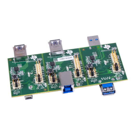
Figure 2-1. TUSB217AEVM-BC..................................................................................................................................................
Figure 6-1. TUSB217AEVM-BC Block Diagram..........................................................................................................................
Figure 6-2. TUSB217AEVM-BC Mini-B Receptacle Section.......................................................................................................
Figure 6-3. TUSB217AEVM-BC Type-B Receptacle Section......................................................................................................
Table 4-2. 3 × 3 Boost Header.....................................................................................................................................................
Table 4-3. 3 × 3 RX_SEN
Header................................................................................................................................................4
Table 4-4. RX_SEN, BOOST Setting Based on Cable Length....................................................................................................
Trademarks
All trademarks are the property of their respective owners.
SLLU327 - MAY 2020
Submit Document Feedback
ABSTRACT
Table of Contents
Levels...........................................................................................................................................4
TUSB217A.........................................................................................................................4
(BOM)........................................................................................................................10
List of Figures
Section.................................................................................................................9
List of Tables
Pinout..............................................................................................................................3
BOM.........................................................................................................................................10
Copyright © 2021 Texas Instruments Incorporated
Table of Contents
TUSB217AEVM-BC Evaluation Module
2
2
3
5
6
2
6
7
8
3
4
1
Advertisement
Table of Contents

Subscribe to Our Youtube Channel
Related Manuals for Texas Instruments TUSB217AEVM-BC


Summary of Contents for Texas Instruments TUSB217AEVM-BC
-
Page 1: Table Of Contents
7 TUSB217AEVM-BC Bill of Materials (BOM)........................10 List of Figures Figure 2-1. TUSB217AEVM-BC..............................Figure 6-1. TUSB217AEVM-BC Block Diagram.......................... Figure 6-2. TUSB217AEVM-BC Mini-B Receptacle Section....................... Figure 6-3. TUSB217AEVM-BC Type-B Receptacle Section...................... Figure 6-4. TUSB217AEVM-BC Type-A Plug Section.........................9 List of Tables Table 4-1. 6 × 2 Configuration Header Pinout..........................3... -
Page 2: Tusb217Aevm-Bc
DCP/CDP pin. The TUSB217AEVM-BC was designed to be used as a path connection between a USB 2.0 host and a USB 2.0 device. The EVM is designed to provide multiple connector options to help eliminate the use of adapters. The upstream interface to the EVM consists of three possible input connectors: a USB 2.0 Mini-B Receptacle, a USB... -
Page 3: Tusb217Aevm-Bc Kit Contents
4 EVM Configuration 4.1 Setting EVM Jumpers The TUSB217AEVM-BC has two 3 × 3 headers and a 6 × 2 header in each board partition to facilitate configuration changes. The BOOST and RX_SEN 3 × 3 headers are arranged to allow for all possible device configurations, including connecting RX_SEN to an LED so that the ENA_HS status output can be viewed easily. -
Page 4: Selecting Configuration Levels
The DCP/CDP pin of the TUSB217A is a battery charging 1.2 Dedicated Charging Port (DCP) and Charging Downstream Port (CDP) function enable. In the shared TUSB216IEVM and TUSB217AEVM-BC schematic, this pin is listed as CDP_ENZ. By default, the TUSB217A has the battery charging 1.2 CDP function enabled with a 500-kΩ... -
Page 5: Evm Operation
Power cycle the VCC_EXT_Px to the EVM or disconnect and reconnect the downstream device Note The VBUS toggle circuit on the TUSB217AEVM-BC should not be used as a reference design. The resistor divider used to sense upstream VBUS will back drive voltage on upstream VBUS due to the internal pullup on DCP/CDP. -
Page 6: Tusb217Aevm-Bc Schematics
TUSB217AEVM-BC Schematics www.ti.com 6 TUSB217AEVM-BC Schematics Figure 6-1 through Figure 6-4 show the EVM schematics. Figure 6-1. TUSB217AEVM-BC Block Diagram TUSB217AEVM-BC Evaluation Module SLLU327 – MAY 2020 Submit Document Feedback Copyright © 2021 Texas Instruments Incorporated... -
Page 7: Figure 6-2. Tusb217Aevm-Bc Mini-B Receptacle Section
TUSB217AEVM-BC Schematics Figure 6-2. TUSB217AEVM-BC Mini-B Receptacle Section SLLU327 – MAY 2020 TUSB217AEVM-BC Evaluation Module Submit Document Feedback Copyright © 2021 Texas Instruments Incorporated... -
Page 8: Figure 6-3. Tusb217Aevm-Bc Type-B Receptacle Section
TUSB217AEVM-BC Schematics www.ti.com Figure 6-3. TUSB217AEVM-BC Type-B Receptacle Section TUSB217AEVM-BC Evaluation Module SLLU327 – MAY 2020 Submit Document Feedback Copyright © 2021 Texas Instruments Incorporated... -
Page 9: Figure 6-4. Tusb217Aevm-Bc Type-A Plug
TUSB217AEVM-BC Schematics Figure 6-4. TUSB217AEVM-BC Type-A Plug Section SLLU327 – MAY 2020 TUSB217AEVM-BC Evaluation Module Submit Document Feedback Copyright © 2021 Texas Instruments Incorporated... -
Page 10: Tusb217Aevm-Bc Bill Of Materials (Bom)
TUSB217AEVM-BC Bill of Materials (BOM) www.ti.com 7 TUSB217AEVM-BC Bill of Materials (BOM) Table 7-1 displays the EVM BOM. Table 7-1. TUSB217AEVM-BC BOM Item Quantity Reference Part C1, C4, C5, C8, C9, C12, C15, C16, C18, C19, C23, C26, C27, C29, 0.1uF... - Page 11 STANDARD TERMS FOR EVALUATION MODULES Delivery: TI delivers TI evaluation boards, kits, or modules, including any accompanying demonstration software, components, and/or documentation which may be provided together or separately (collectively, an “EVM” or “EVMs”) to the User (“User”) in accordance with the terms set forth herein.
- Page 12 www.ti.com Regulatory Notices: 3.1 United States 3.1.1 Notice applicable to EVMs not FCC-Approved: FCC NOTICE: This kit is designed to allow product developers to evaluate electronic components, circuitry, or software associated with the kit to determine whether to incorporate such items in a finished product and software developers to write software applications for use with the end product.
- Page 13 www.ti.com Concernant les EVMs avec antennes détachables Conformément à la réglementation d'Industrie Canada, le présent émetteur radio peut fonctionner avec une antenne d'un type et d'un gain maximal (ou inférieur) approuvé pour l'émetteur par Industrie Canada. Dans le but de réduire les risques de brouillage radioélectrique à...
- Page 14 www.ti.com EVM Use Restrictions and Warnings: 4.1 EVMS ARE NOT FOR USE IN FUNCTIONAL SAFETY AND/OR SAFETY CRITICAL EVALUATIONS, INCLUDING BUT NOT LIMITED TO EVALUATIONS OF LIFE SUPPORT APPLICATIONS. 4.2 User must read and apply the user guide and other available documentation provided by TI regarding the EVM prior to handling or using the EVM, including without limitation any warning or restriction notices.
- Page 15 Notwithstanding the foregoing, any judgment may be enforced in any United States or foreign court, and TI may seek injunctive relief in any United States or foreign court. Mailing Address: Texas Instruments, Post Office Box 655303, Dallas, Texas 75265 Copyright © 2019, Texas Instruments Incorporated...
- Page 16 TI products. TI’s provision of these resources does not expand or otherwise alter TI’s applicable warranties or warranty disclaimers for TI products.IMPORTANT NOTICE Mailing Address: Texas Instruments, Post Office Box 655303, Dallas, Texas 75265 Copyright © 2021, Texas Instruments Incorporated...
Need help?
Do you have a question about the TUSB217AEVM-BC and is the answer not in the manual?
Questions and answers