Table of Contents
Advertisement
Quick Links
ORDER NO. KMS0304716C8
4-Channel Cell Station Unit for DECT Portable Station
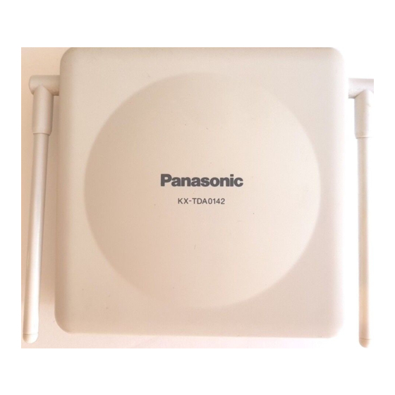
KX-TDA0142CE
(for Europe, Asia Oceania, Middle Near East, Russia and Africa)
2003 Panasonic Communications Co., Ltd. All rights reserved.
Unauthorized copying and distribution is a violation of law.
IMPORTANT INFORMATION ABOUT LEAD FREE, (PbF), SOLDERING
If lead free solder was used in the manufacture of this product the printed circuit boards will be
marked PbF.
Standard leaded, (Pb), solder can be used as usual on boards without the PbF mark.
When this mark does appear please read and follow the special instructions described in this
manual on the use of PbF and how it might be permissible to use Pb solder during service and
repair work.
1. ABOUT LEAD FREE SOLDER (PbF: Pb free)
Note:
In the information below, Pb, the symbol for lead in the periodic table of elements, will refer to
1
PDF created with pdfFactory Pro trial version
www.pdffactory.com
Advertisement
Table of Contents

Subscribe to Our Youtube Channel
Related Manuals for Panasonic KX-TDA0142CE


Summary of Contents for Panasonic KX-TDA0142CE
- Page 1 4-Channel Cell Station Unit for DECT Portable Station KX-TDA0142CE (for Europe, Asia Oceania, Middle Near East, Russia and Africa) 2003 Panasonic Communications Co., Ltd. All rights reserved. Unauthorized copying and distribution is a violation of law. IMPORTANT INFORMATION ABOUT LEAD FREE, (PbF), SOLDERING If lead free solder was used in the manufacture of this product the printed circuit boards will be marked PbF.
-
Page 2: Suggested Pbf Solder
standard solder or solder that contains lead. We will use PbF when discussing the lead free solder used in our manufacturing process which is made from Tin, (Sn), Silver, (Ag), and Copper, (Cu). This model, and others like it, manufactured using lead free solder will have PbF stamped on the PCB. -
Page 3: For Service Technicians
“PbF” is marked on the PCB to show that Pb free solder is used. (See the figure below.) 1.2. NOTE Current models of the KX-TDA0142CE use PbF. Early-production models do not. 2. FOR SERVICE TECHNICIANS ICs and LSIs are vulnerable to static electricity. -
Page 4: Connecting The Cell Station To The Hybrid Ip-Pbx
Item Description Multi Carrier TDMA-TDD Radio Access Method Frequency Band 1880 MHz to 1900 MHz* The number may vary depending on the area . In Taiwan, it is 1880 MHz to 1895 MHz.) Number of Carriers The number may vary depending on the country /area . In Taiwan, is 8.) 1728 kHz Carrier Spacing... - Page 5 Notes - Pin assingnments for the ports 2 to 8 are the same as those of the port 1. Accessory and User-supplied ltems for the CS Accessory: screw x 2, washer x 2, ferrite core x 1. User-supplied: RJ11 connector 5.1.
- Page 6 2. Pass the cable through the groove of the CS (in any direction depending on your convenience). Wrap the cable once around the ferrite core .Then close the case of the ferrite core. PDF created with pdfFactory Pro trial version www.pdffactory.com...
- Page 7 Note If you need to open the ferrite core, use a flathead screwdriver to unlatch the case of the ferrite core. PDF created with pdfFactory Pro trial version www.pdffactory.com...
- Page 8 6. DISASSEMBLY INSTRUCTIONS 1. Remove 5 Screws (A). 2. Remove the Bottom Cabinet. 2. Remove the Solder on Cable of the Main Board by the Soldering iron. PDF created with pdfFactory Pro trial version www.pdffactory.com...
- Page 9 3. Remove the Main Board from the Front Cabinet. 2. Remove the RF unit from the Main Board. 7. TROUBLESHOOTING GUIDES 7.1. Portable Station (PS) cannot register to cell station (CS) or PS does not link CS. PDF created with pdfFactory Pro trial version www.pdffactory.com...
- Page 10 7.2. RF check flowchart for Cell Station (CS) PDF created with pdfFactory Pro trial version www.pdffactory.com...
- Page 11 PDF created with pdfFactory Pro trial version www.pdffactory.com...
- Page 12 PDF created with pdfFactory Pro trial version www.pdffactory.com...
- Page 13 3. Service Jip cable (PSZZ2TDA0142) 4. AC Adaptor or Battery Box (PSZZTD142CE) 8.1. Initial setting 1.1 Connect KX-TDA0142CE to your PC with the Service JIG cable, and then power on KX- TDA0142CE with a Power supply adaptor. 1.2 Property Please set property as follows...
- Page 14 Please set as follows. 2.1 How to enter “CS login mode”. After waiting for about 10 seconds, press Ctrl and “D” simultaneously to enter “CS login mode” (The following window is displayed.). 2.2. Press “VER” and Enter, then software version is appeared on display. If version of TDA0142CE is appeared, then operation of CPU is OK.
-
Page 15: Test And Adjustment
1. Connect KX-TDA0142CE (Cell Station) with cable between CS and CSINF card. 2. Connect PBX and PC with USB or Serial cable, then execute “PC programming”. 3. Press “Configuration” and “CSINF Port”. 4. Confirm Cell Station Status. INS: In Service... - Page 16 9.1.2. RF test 9.1.2.1. Preparation for RF test 1. Remove the under cabinet (Refer to 6. DISASSEMBLY INSTRUCTION 1.) PDF created with pdfFactory Pro trial version www.pdffactory.com...
- Page 17 2. Remove 2 antennas from CN103 and CN104 (Refer to 6. DISASSEMBLY INSTRUCTION 2.) 3. Remove the P.C.B from upper cabinet (Refer to 6. DISASSEMBLY INSTRUCTION 3.) 4. Solder cable to ANT1(CN103) (Refer to figure) 5. CMD60 set up. TEST MODE CONFIG MENU SIGN.
- Page 18 must be ±259 to ±403kHz. 9. Check the Frequency Drift : must be 0 ±35kHz/ms. 10. Press MENU UP " " on the CMD60. 11. Press POWER RAMP. 12. Check the Burst fits mask. 13. Press MENU UP " " on the CMD60. 14.
- Page 19 Set CMD60 into RF-generator mode. Default Display MODULE TEST RFGEN Default After setting FREQ./RF CHAN. 1897.344MHz (0CH) 1888.704MHz (5CH) DEVIATION 288kHz 0kHz SIGNAL CONST.ENVELOP CONST.ENVELOP (00001111) (00001111) RF LEVEL -40 dBm -40 dBm 6. Set Dip switch all pins to OFF. 7.
- Page 20 serial port setup check next check boxes ASCII Sending - Sending line ends with line feeds ASCII Receiving - Append line feeds to incoming line ends Warp lines that exceed terminal width 10. Supply a voltage to the TEL jack from the AC adaptor (KX-TCA1) / via power supply adaptor (PSZZ1TDA0142) 9.1.3.2.
- Page 21 9.2. ADJUSTMENT FOR MAIN PART 9.2.1. Required Equipments 1. Frequency counter 2. (PC) Personal Computer with serial port (Windows 2000/98 or previous version) 3. Power supply adaptor (PSZZ1TDA0142) 4. Service JIG cable (PSZZ2TDA0142) 5. AC Adaptor (KX-TCA1) or Battery Box (PSZZTD142CE) PDF created with pdfFactory Pro trial version www.pdffactory.com...
- Page 22 9.2.2. Preparation 1. Remove the under cabinet (Refer to 6. DISASSEMBLY INSTRUCTIONS) 2. Remove 2 antennas from CN3 and CN104 (Refer to 6. DISASSEMBLY INSTRUCTIONS) 3. Remove the P.C.B from the upper cabinet (Refer to 6. DISASSEMBLY INSTRUCTIONS) 4. Connect PC to the CS by service JIG cable 5.
- Page 23 (also refer to 8.1. initial setting) serial port setup Port COM1 Bit per second 19200 Data bits Parity None Stop bit Flow control Xon/Xoff serial port setup check next check boxies ASCII Sending - Sending line ends with line feeds ASCII Receiving - Append line feeds to incoming line ends Warp line that exceed terminal width...
-
Page 24: Frequency Table (Mhz)
1) Send “Read command to non-volatile memory” and read current status. Command: 122600000204 Response: 0F5601040000XX00 XX:Current value 2) Measure frequency at SYRI test point. (SYRI-GND) (Refer to PRINTED CIRCUIT BOARD 21.2 Bottom View p46) If measured frequency is within the range of 10.368 MHz ±20 Hz, proceed to step 5. 3) Read “Clock frequency set - command”, and set calibration data. -
Page 25: Hardware Description
12. HARDWARE DESCRIPTION 12.1. FUNCTION DESCRIPTION KX-TDA0142CE is the Cell Station (CS) for TDA series. CS converts voice data from PBX to radio signal and transmits to Portable Station (PS). Conversely CS converts radio signal from PS to voice data and transmits to PBX. - Page 26 signal and 4MHz clock) and digital data in ST-BUS format from the analog signal provided by PBX. These clocks and digital data is transferred to FPGA (IC101) and HDLC control IC (IC112). HDLC means High Level Data Line Control, a protocol for highly reliable data communication. This ST-BUS digital data contains data channel, control channel and voice channel.
- Page 27 Extracts voice data from ST-BUS digital data and changes format to IOM-2 format, then provides to BBIC. (2) Superframe detection, delay compensation Detects super frame synchronization signal from HK bit in the ST-BUS digital data and compensates time difference of delay caused by the different cable length from CSIF card, then provides to PSYNC pin of BBIC.
-
Page 28: Power Supply Circuit
BBIC PMB4729 manufactured by Infineon GAUSSIAN FILTER Gaussian filter is used for pulse shaping of TXDA signal that is sent from BBIC to RF module. LEVEL SHIFTER Level shifter is used for voltage matching of RXDA from RF module to BBIC. RSSI HOLD CIRCUIT RSSI signal from RF module is hold at this circuitry and fed to A/D port of the CPU. -
Page 29: Clock Circuit
INPUT FILTER, DIODE BRIDGE Input filter for noise rejection and diode bridge for misconnection protection. DC/DC START UP CONTROL CIRCUIT This circuit control start up of DC/DC converter IC for the quick recovery from power interruption. DC/DC CONVERTER CIRCUIT Generate 5.0V from DC40V power supply. POWER BACK UP CIRCUIT All power supply is back- upped by the primary electrolyte capacitor and secondary super capacitor. - Page 30 13. IC DATA 13.1. IC100 (BBIC) Description High High- Low Pin Description High High- Fixed VDD0 PSYNC Active Normal 53 SYRI Active Active Active Active 54 EXTAL Active Active Active Active 55 XTAL Active Active Active Active 56 VSS0 Active Active 57 MODE Fixed...
- Page 31 Description High High- Low Pin Description High High- VDDPLL RXDSG Active Normal RESETQ Active Normal 77 no use (RXOFF) Normal Active Active 78 RXDA Active Active Active 79 TXDA Active Active Active Active 80 PAON Normal Active Active Normal 81 83 no use (ADPFR) VDD5 84 no use (ADPCL)
- Page 32 Description High High- Description High High- VCC0 Active Fixed Active (0V) HWRN Active CS_I Normal Active Active Normal Active Active Active Active DSTO Active Active Active DSTI Active no use (HDLCIRQ) VCCINT 65 no use (CS6N) Active Active 66 no use (CS5N) Active Active CS4N...
- Page 33 94 no use (RXA) Description High High- Description High High- Active Active RSTN for Normal HDLC Active Active 96 RDN for HDLC Normal Active Active VCCINT RSTN Normal Active Active Active A3 for HDLC Active no use 100 A2 for HDLC Active (PCMIN) 101 A1 for HDLC...
- Page 34 Description High High- Description High High- 113 D5 for HDLC Active Active 129 A8 for BBIC Active 114 D4 for HDLC Active Active 130 A7 for BBIC Active 115 D3 for HDLC Active Active 131 A6 for BBIC Active 116 D2 for HDLC Active Active 132 A5 for BBIC Active...
- Page 35 Description High High- Description High High- Active Active 51 Active Active Active 52 Active soft reset Active Normal 53 Active FPGA reset Normal Active 54 no use (P20) Fixed (3.3V) DC/DC stop Active Normal 55 FPGA Normal PROGRAM BBIC reset Normal Active 56 FPGA DONE...
-
Page 36: How To Replace A Flat Package Ic
Description High High- Description High High- Active Active 84 Fixed (3.3V) Active Active 85 Active Active 86 DAC for OSC TRIM Active Active 87 AVSS Active Active 88 Active Active 89 input port for Normal DIP SW5 input port for Normal DIP SW6 Active... - Page 37 Recommended Flux: Specific Gravity 0.863. (Original flux should be replaced daily.) 14.1.2. PbF Solder - Soldering Iron Tip Temperature of 700°F ± 20°F (370°C ± 10°C) Note: We recommend a 30 to 40 Watt soldering iron. An expert may be able to use a 60 to 80 Watt iron where someone with less experience could overheat and damage the PCB foil.
-
Page 38: Removing Solder From Between Pins
tip so that it flows under the pins as they are heated. 14.3. REMOVING SOLDER FROM BETWEEN PINS 1. Add a small amount of solder to the bridged pins. 2. With a hot iron, use a sweeping motion along the flat part of the pin to draw the solder from between the adjacent pads. -
Page 39: Cabinet And Electrical Parts Location
16. CABINET AND ELECTRICAL PARTS LOCATION PDF created with pdfFactory Pro trial version www.pdffactory.com... -
Page 40: Accessories And Packing Materials
17. ACCESSORIES AND PACKING MATERIALS PDF created with pdfFactory Pro trial version www.pdffactory.com... - Page 41 PDF created with pdfFactory Pro trial version www.pdffactory.com...
-
Page 42: Replacement Parts List
18. REPLACEMENT PARTS LIST 1. RTL (Retention Time Limited) Note : The marking (RTL) indicates that the Retention Time is limited for this item. After the discontinuation of this assembly in production, the item will continue to be available for a specific period of time. The retention period of availability is depends on the type of assembly, and in accordance with the laws governing parts and product retention. -
Page 43: Main Board Parts
18.1. CABINET AND ELECTRICAL PARTS LOCATION Ref. No. Part No. Part Name & Description Remarks PSKM1036W1 CABINET BODY ABC-94HB N1CAAJY00004 ANTENNA PSHX1128Z COVER PSKF1064Z1 CABINET COVER ABC-94HB PSHG1063Z RUBBER PARTS KR16TT100510 MAGNET PSGT2218X NAME PLATE 18.2. ACCESSORIES AND PACKING MATERIALS Ref. - Page 44 Ref. No. Part No. Part Name & Description Remarks PCB1 PSWPA0142CEU MAIN BOARD ASS'Y (RTL) (ICS) IC100 PQVIPMB4729T IC101 C1ZBZ0001996 IC102 PQVI2340FA10 IC103 C3FBKD000181 IC104 PQWP2CD650CE IC (RF UNIT) IC105 PQVIBS2L1ST IC108 C0EBE0000117 IC109 PQVIMC7101B5 IC110 PQVITC7WU04F IC111 PSVIHDLV74TE IC112 PSVIMT8952BP IC113 C1CB00001191...
- Page 45 Ref. No. Part No. Part Name & Description Remarks X101 H1B1925B0021 CONNECTOR (JACK) JK100 PSJJ1T011Z JACK (CERAMIC FILTERS) FIL3 PSVFNBMK200T CERAMIC FILTER FIL6 J0HAAH000003 CERAMIC FILTER FIL7 J0HAAH000003 CERAMIC FILTER FIL8 J0HAAH000003 CERAMIC FILTER FIL9 J0HAAH000003 CERAMIC FILTER FIL10 J0HAAH000003 CERAMIC FILTER FIL11 J0HAAH000003...
- Page 46 Ref. No. Part No. Part Name & Description Remarks R107 ERJ3GEY0R00 R108 ERJ3GEY0R00 R109 ERJ3GEY0R00 R111 ERJ3GEY0R00 R113 ERJ3GEYJ271 R115 ERJ3GEYJ102 R116 ERJ3GEYJ103 R117 ERJ3GEYJ473 R118 ERJ3GEYJ473 R119 ERJ3GEYJ473 R120 ERJ3GEYJ473 R121 ERJ3GEYJ103 R122 ERJ3GEYJ103 R123 ERJ3GEYJ102 R124 ERJ3GEYJ102 R126 ERJ3GEYJ104 100k R128...
- Page 47 Ref. No. Part No. Part Name & Description Remarks R177 ERJ3GEYJ330 R178 ERJ3GEYJ104 100k R179 ERJ3GEYJ104 100k R180 ERJ3GEYJ104 100k R181 ERJ3GEYJ104 100k R182 ERJ3GEYJ104 100k R183 ERJ3GEYJ104 100k R184 ERJ3GEYJ104 100k R185 ERJ3GEYJ104 100k R186 ERJ3GEYJ104 100k R187 ERJ3GEYJ104 100k R188 ERJ3GEYJ104...
- Page 48 Ref. No. Part No. Part Name & Description Remarks R254 ERJ3GEYJ473 R255 ERJ3GEYJ473 R256 ERJ3GEYJ473 R257 ERJ3GEYJ473 R258 ERJ3GEYJ473 R259 ERJ3GEYJ473 R260 ERJ3GEYJ473 R261 ERJ3GEYJ473 R262 ERJ3GEYJ473 R263 ERJ3GEYJ473 R264 ERJ3GEYJ473 R265 ERJ3GEYJ473 R267 ERJ3GEYJ473 R268 ERJ3GEYJ473 R269 ERJ3GEYJ473 R270 ERJ3GEYJ473 R271 ERJ3GEYJ473...
- Page 49 Ref. No. Part No. Part Name & Description Remarks R325 ERJ3GEYJ102 R326 ERJ3GEYJ102 R327 ERJ3GEYJ102 R329 ERJ3GEYJ101 R330 ERJ3GEYJ101 R335 ERJ3GEYJ473 R339 ERJ3GEYJ391 R340 ERJ3GEYJ470 R344 ERJ3GEYJ473 R345 ERJ3GEYF472 4.7k R346 ERJ3GEYF152V 1.5k R348 ERJ3GEYJ123 R349 ERJ14YJ121 R350 ERJ3GEYJ330 R351 ERJ3GEYJ330 R352 ERJ3GEYJ330...
- Page 50 Ref. No. Part No. Part Name & Description Remarks R427 ERJ3GEY0R00 RA100 D1H83304A010 RA101 D1H83304A010 RA102 D1H83304A010 RA103 D1H83304A010 RA104 D1H83304A010 RA105 D1H83304A010 RA106 D1H83304A010 RA107 D1H83304A010 RA108 D1H83304A010 RA109 D1H83304A010 C100 ECUV1H100DCV 10p C101 ECUV1H100DCV 10p C102 ECUV1H100DCV 10p C103 ECUV1H100DCV 10p C104...
- Page 51 Ref. No. Part No. Part Name & Description Remarks C154 ECUV1H270JCV C155 ECUV1H100DCV 10p C156 ECUV1H151JCV 150p C158 ECUV1E104ZFV C159 ECUV1H471JCV 470p C160 ECUV1H103KBV 0.01 C161 ECUV1H471JCV 470p C162 ECUV1H103KBV 0.01 C163 ECUV1H471JCV 470p C164 ECUV1H103KBV 0.01 C165 ECUV1H471JCV 470p C166 ECUV1H103KBV 0.01 C167...
-
Page 52: Fixtures And Tools
Ref. No. Part No. Part Name & Description Remarks C221 ECUV1H471JCV 470p C222 ECUV1H100DCV 10p C223 ECUV1H100DCV 10p C224 ECUV1H152KBV 0.0015 C225 ECUV1E223KBV 0.022 C226 ECUV1C334ZFV 0.33 C227 ECUV1E104ZFV C228 ECUV1E104ZFV C229 ECUV1H103KBV 0.01 C230 ECUV1H471JCV 470p C238 ECUV1E104ZFV C239 F2G0J4710005 C240 EECFE5R5474... - Page 53 2. The schematic diagrams and circuit board may be modified at any time with the development of new technology. 20. SCHEMATIC DIAGRAM (MAIN) 21. PRINTED CIRCUIT BOARD(MAIN) 21.1. Component View 21.2. Bottom View Y.M / KXTDA0142CEUK PDF created with pdfFactory Pro trial version www.pdffactory.com...
- Page 54 Loop filter To CPU Block :32/33 :N/A DRON PAON SYRI SYCL RXON Stand by & PLL & LC Filter SYDA D400 Control logic Control logic SYEN BAR64- RXDSG RXDA Demodulator Low IF bandpass filter RSSI S&H IC402 PMB6610 KX-TDA0142CE RF BLOCK...
- Page 55 CK299 CK310 HDD[5] HDD[6] R259 HDD[3] R250 CK300 CK311 HDD[6] HDD[7] R251 R260 HDD[4] CK301 CK312 HDD[7] R261 HDD[5] CK302 R262 HDD[6] CK303 R263 HDD[7] CK304 (B) (D) (H)(J) (L) KX-TDA0142CE MAIN BOARD 1/4 (A) (C) (F) (G) (I) (K)
- Page 56 D118 IC115 CK468 CK467 R391 330u CK487 1/4W120 +VIN 1/4W15 CK463 FEEDBACK CK537 CK525 OUTPUT Q112 CK457 /ON/OFF CK466 Q114 CK461 DC/DCCONVERTER CK465 CK464 CK363 CK469 R390 CK488 R394 Q113 104ns 3.3V 3.3V 250ns DSTI DSTO KX-TDA0142CE MAIN BOARD 2/4...
- Page 57 CK206 VCCINT 38 GND 3.3V CK207 39 GND 2.4s 2.4s 40 GND CK209 CK208 R146 R145 TRIM 41 GND 96ns 42 GND 43 GND L109 C272 3.3V 44 RF1 45 GND 3.3V 125µs KX-TDA0142CE MAIN BOARD 3/4 (P)(Q) (R) (S)
- Page 58 CK240 1000P R166 10K X101 D3R3V IC110 D3R3V D3R3V IC111 CK474 HCU04 CK473 IC110 IC111 IC110 CK483 HCU04 CLK 11 RF3R3V CK486 CK600 FIL5 Q107 CK601 IC200 R369 D3R3V Vout R427 52ns CK454 D108 2.2V XC62EP3302 KX-TDA0142CE MAIN BOARD 4/4...
- Page 59 RA108 R254 RA106 R255 RA104 C214 C215 R308 R113 R196 C240 FIL10 C120 R411 R328 FIL1 C121 FIL2 R140 C286 R138 C122 IC100 R352 R114 R351 R115 R350 R353 R354 R355 R144 X100 R170 PSUP1381YB KX-TDA0142CE MAIN BOARD COMPONENT VIEW...
- Page 60 C129 R136 C118 C142 C280 R107 C141 C133 C134 C161 R137 C287 PSYCPU C164 R199 C162 TXDA C165 D2R5V C137 C167 D118 R173 R195 C136 C138 C159 R177 C135 C160 C168 C158 R349 R145 BXTL KX-TDA0142CE MAIN BOARD BOTTOM VIEW...
- Page 62 CS ON Line Debbuger Vxx.xx Start...
- Page 63 CS ON Line Debbuger Vxx.xx Start CS VER BOOT Ver **. ** 2002 10 Ver **. ** 2002 10...
- Page 64 BLOCK DIAGRAM of KX-TDA0142CE CPU board Base Band IC PMB4729 (IC100) IOM-2 Burst Mode 2x Echo ADPCM Controller Canceller RF Interface TX/RX 3.3V DTMF Generator 2x C-ID & Receiver 4x Echo Suppresor 2x PMB2920 I/F 4x PCM I/F uC I/F 10.24M (X102)
Need help?
Do you have a question about the KX-TDA0142CE and is the answer not in the manual?
Questions and answers