Table of Contents
Advertisement
Quick Links
RH850 Evaluation Platform
RH850/F1x-176pin
PiggyBack board V3
32
Y-RH850-F1X-176PIN-PB-T1-V3
All information contained in these materials, including products and product specifications,
represents information on the product at the time of publication and is subject to change by
Renesas Electronics Corp. without notice. Please review the latest information published by
Renesas Electronics Corp. through various means, including the Renesas Technology Corp.
website (http://www.renesas.com).
The newest version of this document can be obtained from the following web location
http://www.renesas.eu/updates?oc=Y-RH850-F1X-176PIN-PB-T1-V3
www.renesa s.com
R20UT3931ED0120, Rev. 1.20
2017-10-20
Advertisement
Table of Contents

Related Manuals for Renesas Y-RH850-F1X-176PIN-PB-T1-V3


Summary of Contents for Renesas Y-RH850-F1X-176PIN-PB-T1-V3
- Page 1 All information contained in these materials, including products and product specifications, represents information on the product at the time of publication and is subject to change by Renesas Electronics Corp. without notice. Please review the latest information published by Renesas Electronics Corp. through various means, including the Renesas Technology Corp.
-
Page 4: Table Of Contents
Table of Contents Chapter 1 Introduction ................. 5 Chapter 2 Overview ................6 Overview ....................6 Mounting of the device ................ 7 Chapter 3 Jumper Configuration ............8 Chapter 4 Power supply ..............10 Board power connection ..............10 Voltage distribution ................11 Chapter 5 Clock sources .............. -
Page 5: Chapter 1 Introduction
Renesas Electronics 32-bit RH850/F1x microcontrollers. The piggyback board (Y-RH850-F1X-176PIN-PB-T1-V3) can be used as a standalone board, or can be mated with a mainboard (e.g. Y-RH850-X1X-MB-Tx-Vx) for extended functionality. -
Page 6: Chapter 2 Overview
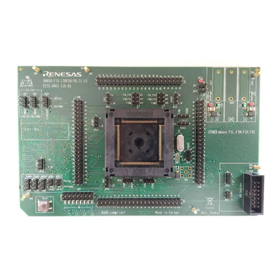
RH850/F1x-176pin PiggyBack board V3 Y-RH850-F1X-176PIN-PB-T1-V3 Chapter 2 Overview 2.1 Overview Figures 1 and 2 provide the views of the Piggyback Board (EESS-0400-135-02). Figure 1 – PiggyBoard top view Figure 2 – PiggyBoard bottom view R20UT3931ED0120 Rev. 1.20 2017-10-20... -
Page 7: Mounting Of The Device
RH850/F1x-176pin PiggyBack board V3 Y-RH850-F1X-176PIN-PB-T1-V3 2.2 Mounting of the device The board is designed for use with the following devices (each in the 176pin package version): RH850/F1L RH850/F1M RH850/F1H RH850/F1K RH850/F1KM-S4 The device must be placed inside the socket IC1. To insert the device, press down the lid, align the #1 pin of the device to the #1pin of the socket, insert the device inside the socket and release the lid. -
Page 8: Chapter 3 Jumper Configuration
RH850/F1x-176pin PiggyBack board V3 Y-RH850-F1X-176PIN-PB-T1-V3 Chapter 3 Jumper Configuration The function of the board can be configured via jumpers. This chapter describes the standard configuration, i.e. jumper setting for the intended devices. For the supported function of the used device, please refer to the corresponding HW user’s manual. - Page 9 RH850/F1x-176pin PiggyBack board V3 Y-RH850-F1X-176PIN-PB-T1-V3 The jumper setting also are shown in this picture: Figure 3 – Jumper setting overview JP25 for FLMDO0 always must be closed for a ‘normal’ green jumper (user mode and debug) operation of the device.
-
Page 10: Chapter 4 Power Supply
RH850/F1x-176pin PiggyBack board V3 Y-RH850-F1X-176PIN-PB-T1-V3 Chapter 4 Power supply 4.1 Board power connection For operation of the device, a supply voltage must be connected to the board. Though a single supply voltage is sufficient for the operation of the device, two (different) voltages can be supplied to the board. -
Page 11: Voltage Distribution
RH850/F1x-176pin PiggyBack board V3 Y-RH850-F1X-176PIN-PB-T1-V3 4.2 Voltage distribution The table shows the required device power supply pins and their function: Device Name on supply Function PiggyBoard REGVCC REGVDD Supply for the device internal regulators for the digital logic. EVCC EVDD Supply for ports. -
Page 12: Chapter 5 Clock Sources
RH850/F1x-176pin PiggyBack board V3 Y-RH850-F1X-176PIN-PB-T1-V3 Chapter 5 Clock sources Three external crystal oscillators for the device clock supply are provided with the board. 5.1 MainOsc A crystal or ceramic resonator can be mounted on socket X1. The applicable frequency range can be found is the devices electrical specification. -
Page 13: Chapter 6 Debug And Programming Interface
RH850/F1x-176pin PiggyBack board V3 Y-RH850-F1X-176PIN-PB-T1-V3 Chapter 6 Debug and Programming interface For connection of the microcontroller debug and flash programming tools, the connector CN19 is provided. The signal connection of the connector CN19 is shown in the picture below: CN19 pin... -
Page 14: Chapter 7 Connectors For Ports Of Device
RH850/F1x-176pin PiggyBack board V3 Y-RH850-F1X-176PIN-PB-T1-V3 Chapter 7 Connectors for ports of device Connection to each pin of the device is possible via the connectors CN5 to CN8. Note: The pin headers are directly connected to the pins of the device, therefore special care must be taken to avoid any electrostatic or other damage to the device. - Page 15 RH850/F1x-176pin PiggyBack board V3 Y-RH850-F1X-176PIN-PB-T1-V3 Function Device Port Function Device Port P10_5 P18_4 ETH0RXD3 EH0TXD3 ETH0RXDCLK P10_0 P18_7 ETH0TXCLK P11_14 or P18_6 ETH0RXER ETH0TXER P11_15 P11_13 P18_5 ETH0CRSDV ETH0TXEN P11_11 P11_10 ETH0RXDV ETH0COL P2_6 ETH0RESET ETH0LINK P18_0 USB0UDMF USB0UDMH USB0UDPF...
-
Page 16: Connector Cn2
RH850/F1x-176pin PiggyBack board V3 Y-RH850-F1X-176PIN-PB-T1-V3 7.1.2 Connector CN2 Function Device Port Function Device Port CAN2Tx P12_0 CAN3Tx P1_3 CAN2Rx P11_15 CAN3Rx P1_2 CAN4Tx P1_13 CAN5Tx P11_6 CAN4Rx P1_12 CAN5Rx P11_5 LIN2Tx P0_10 LIN3Tx P1_15 LIN2Rx P0_9 LIN3Rx P1_14 LIN4Tx P1_11... - Page 17 RH850/F1x-176pin PiggyBack board V3 Y-RH850-F1X-176PIN-PB-T1-V3 Function Device Port Function Device Port Not available on the EESS-0400-135-01 board version. R20UT3931ED0120 Rev. 1.20 2017-10-20...
-
Page 18: Connector Cn3
RH850/F1x-176pin PiggyBack board V3 Y-RH850-F1X-176PIN-PB-T1-V3 7.1.3 Connector CN3 Function Device Port Function Device Port PWM00 P10_0 PWM01 P10_1 PWM02 P10_2 PWM03 P10_3 PWM04 P10_7 PWM05 P10_8 PWM06 P10_9 PWM07 P10_10 PWM08 P9_0 PWM09 P9_1 PWM10 P0_4 PWM11 P0_1 PWM12 P0_2... - Page 19 RH850/F1x-176pin PiggyBack board V3 Y-RH850-F1X-176PIN-PB-T1-V3 Function Device Port Function Device Port PWMADC02 AP0_10 PWMADC03 AP0_11 PWMADC04 AP0_12 PWMADC05 AP0_13 PWMADC06 AP0_14 PWMADC07 AP0_15 PWMADC08 AP1_0 PWMADC09 AP1_1 PWMADC10 AP1_2 PWMADC11 AP1_3 PWMADC12 AP1_4 PWMADC13 AP1_5 PWMADC14 AP1_6 PWMADC15 AP1_7 R20UT3931ED0120 Rev. 1.20...
-
Page 20: Chapter 8 Other Circuitry
RH850/F1x-176pin PiggyBack board V3 Y-RH850-F1X-176PIN-PB-T1-V3 Chapter 8 Other circuitry 8.1 Push button for RESET In order to issue a RESET to the device, the push-button SW1 is available. 8.2 Mode Selection The PiggyBack Board gives the possibility to configure the following mode pins ... -
Page 21: Chapter 9 Precautions
RH850/F1x-176pin PiggyBack board V3 Y-RH850-F1X-176PIN-PB-T1-V3 Chapter 9 Precautions JP24 signal naming The signal name printed on the PCB top side below JP24 ETH0CRSDV is not correct. The correct signal name as used in the schematic is ETH0RXER (or ETNB0RXERR as it is used in the User’s Manual). -
Page 22: Can6 Signals On Cn2
RH850/F1x-176pin PiggyBack board V3 Y-RH850-F1X-176PIN-PB-T1-V3 CAN6 signals on CN2 On some boards of the version ‘EESS-0400-135-01’ the following rework is not applied: In case your board is affected and you want to make use of the CAN6 functionality via CN2, either of the two solutions can be applied: ... -
Page 23: Chapter 10 Mechanical Dimensions
RH850/F1x-176pin PiggyBack board V3 Y-RH850-F1X-176PIN-PB-T1-V3 Chapter 10 Mechanical dimensions 100,00mm 50,00mm R20UT3931ED0120 Rev. 1.20 2017-10-20... - Page 24 RH850/F1x-176pin PiggyBack board V3 Y-RH850-F1X-176PIN-PB-T1-V3 R20UT3931ED0120 Rev. 1.20 2017-10-20...
-
Page 25: Chapter 11 Schematic
RH850/F1x-176pin PiggyBack board V3 Y-RH850-F1X-176PIN-PB-T1-V3 Chapter 11 Schematic This chapter shows the schematics of the two available board versions: EESS-0400-135-01 EESS-0400-135-02 R20UT3931ED0120 Rev. 1.20 2017-10-20... -
Page 26: Schematic For Eess-0400-135-01
RH850/F1x-176pin PiggyBack board V3 Y-RH850-F1X-176PIN-PB-T1-V3 11.1 Schematic for EESS-0400-135-01 R20UT3931ED0120 Rev. 1.20 2017-10-20... - Page 27 RH850/F1x-176pin PiggyBack board V3 Y-RH850-F1X-176PIN-PB-T1-V3 PUSH BUTTON 4 PIN SMD R20UT3931ED0120 Rev. 1.20 2017-10-20...
- Page 28 RH850/F1x-176pin PiggyBack board V3 Y-RH850-F1X-176PIN-PB-T1-V3 R20UT3931ED0120 Rev. 1.20 2017-10-20...
-
Page 29: Schematic For Eess-0400-135-02
RH850/F1x-176pin PiggyBack board V3 Y-RH850-F1X-176PIN-PB-T1-V3 11.2 Schematic for EESS-0400-135-02 R20UT3931ED0120 Rev. 1.20 2017-10-20... - Page 30 RH850/F1x-176pin PiggyBack board V3 Y-RH850-F1X-176PIN-PB-T1-V3 PUSH BUTTON 4 PIN SMD R20UT3931ED0120 Rev. 1.20 2017-10-20...
- Page 31 RH850/F1x-176pin PiggyBack board V3 Y-RH850-F1X-176PIN-PB-T1-V3 R20UT3931ED0120 Rev. 1.20 2017-10-20...
-
Page 32: Chapter 12 Revision History
RH850/F1x-176pin PiggyBack board V3 Y-RH850-F1X-176PIN-PB-T1-V3 Chapter 12 Revision History The table provides information about the major changes of the document versions. Date Version Description 2016-11-14 1.00 Initial release Corrected jumper setting of JP25 (FLMD0) in figure 3 (chapter 3). - Page 34 Mouser Electronics Authorized Distributor Click to View Pricing, Inventory, Delivery & Lifecycle Information: Renesas Electronics Y-RH850-F1X-176PIN-PB-T1-V3...
Need help?
Do you have a question about the Y-RH850-F1X-176PIN-PB-T1-V3 and is the answer not in the manual?
Questions and answers