Table of Contents
Advertisement
Quick Links
SAMR30 IEEE
Introduction
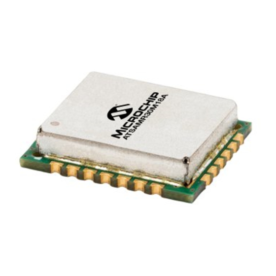
The ATSAMR30M18A is an IEEE
such as 780 MHz (China), 868 MHz (Europe) and 915 MHz (North America), optimized for low-power applications.
This module combines the ATSAMR30E18A SiP (System in Package), 16 MHz crystal oscillator, discrete balun,
lumped element harmonic reject filter and required RF shielding in a compact 12.7 mm x 11.0 mm design. The
module as implemented on the Xplained Pro development board has passed regulatory approvals with chip antenna
or SMA connectorized monopole antenna.
This data sheet provides only a brief overview of the necessary sections of the module. For a detailed description of
each peripheral, refer to the
Features
•
Processor
®
®
– ARM
Cortex
-M0+ CPU running at up to 48 MHz
•
Single-cycle hardware multiplier
•
Micro Trace Buffer (MTB)
•
Memories
– 256 KB in-system self-programmable Flash
– 32 KB SRAM
– 8 KB low-power RAM
•
System
– Power-on Reset (POR) and Brown-out Detection (BOD)
– Internal clock option with 48 MHz Digital Frequency Locked Loop (DFLL48M) and 48 MHz to 96 MHz
Fractional Digital Phase Locked Loop (FDPLL96M)
– External Interrupt Controller (EIC)
– Up to 14 external interrupts
– One non-maskable interrupt
– Two-pin Serial Wire Debug (SWD) programming, test and debugging interface
•
Low Power
– Idle and Standby Sleep modes
– Sleep walking peripherals
•
Integrated Ultra-Low Power Transceiver for 700/800/900 MHz ISM Band:
– Chinese WPAN band from 779 to 787 MHz
– European SRD band from 863 to 870 MHz
– North American ISM band from 902 to 928 MHz
– Japanese band from 915 to 930 MHz
•
Direct Sequence Spread Spectrum with Different Modulation and Data Rates:
– BPSK with 20 and 40 kb/s, compliant to IEEE 802.15.4-2003/2006/2011
– O-QPSK with 100 and 250 kb/s, compliant to IEEE 802.15.4-2006/2011
– O-QPSK with 200, 400, 500 and 1000 kb/s PSDU data rate
©
2018-2021 Microchip Technology Inc.
and its subsidiaries
®
™
802.15.4
®
™
802.15.4
-2003/2006/2011-compliant RF module for the sub-1 GHz ISM bands,
ATSAMR30E18A data
sheet.
ATSAMR30M18A
Sub-1GHz Module Datasheet
Datasheet
DS70005384B-page 1
Advertisement
Table of Contents

Related Manuals for Microchip Technology ATSAMR30M18A


Summary of Contents for Microchip Technology ATSAMR30M18A
-
Page 1: Introduction
Sub-1GHz Module Datasheet Introduction ® ™ The ATSAMR30M18A is an IEEE 802.15.4 -2003/2006/2011-compliant RF module for the sub-1 GHz ISM bands, such as 780 MHz (China), 868 MHz (Europe) and 915 MHz (North America), optimized for low-power applications. This module combines the ATSAMR30E18A SiP (System in Package), 16 MHz crystal oscillator, discrete balun, lumped element harmonic reject filter and required RF shielding in a compact 12.7 mm x 11.0 mm design. - Page 2 Oversampling and decimation in hardware to support 13-, 14-, 15- or 16-bit resolution – Two Analog Comparators (AC) with window compare function – Peripheral Touch Controller (PTC) • 12-Channel capacitive touch and proximity sensing • Clock Datasheet DS70005384B-page 2 © 2018-2021 Microchip Technology Inc. and its subsidiaries...
- Page 3 – RX_ON = 10.79 mA – BUSY_TX = 26.97 mA – Standby = 2.03 µA – Backup mode = 0.77 µA Note: For more details, see 9.3.4 Current Consumption Specifications. Datasheet DS70005384B-page 3 © 2018-2021 Microchip Technology Inc. and its subsidiaries...
-
Page 4: Table Of Contents
11.1. Approved Antennas........................43 11.2. Module Assembly Considerations....................43 12. Application Reference Design.......................44 12.1. RF Trace Layout Design Instructions..................44 12.2. Routing Guidelines........................52 13. Regulatory Approval..........................54 13.1. United States (FCC)........................54 Datasheet DS70005384B-page 4 © 2018-2021 Microchip Technology Inc. and its subsidiaries... - Page 5 The Microchip Website..........................64 Product Change Notification Service......................64 Customer Support............................64 Microchip Devices Code Protection Feature....................64 Legal Notice..............................65 Trademarks..............................65 Quality Management System........................66 Worldwide Sales and Service........................67 Datasheet DS70005384B-page 5 © 2018-2021 Microchip Technology Inc. and its subsidiaries...
-
Page 6: Ordering Information And Module Marking
ATSAMR30M18A Ordering Information and Module Marking Ordering Information and Module Marking The following table provides the ordering details for the ATSAMR30M18A module. Table 1-1. Ordering Information for ATSAMR30M18A Package Number of Regulatory Model Number Ordering Code Description Dimension Pins Approval ATSAMR30M18A-I/... -
Page 7: Package Information
ATSAMR30M18A Package Information Package Information The following table provides the ATSAMR30M18A module package dimensions. Table 2-1. ATSAMR30M18A Package Information Parameter Value Units Package size 12.7 x 11.0 Pad count — Total thickness 2.71 Pad pitch Pad width Datasheet DS70005384B-page 7 ©... -
Page 8: Module Block Diagram
ATSAMR30M18A Module Block Diagram Module Block Diagram The ATSAMR30M18A module contains ATSAMR30E18A SiP, 16 MHz crystal, discrete Balun and lumped element Harmonic Filter. The following figure shows the block diagram of the ATSAMR30M18A module. Figure 3-1. Module Block Diagram 16 MHz... - Page 9 Table 3-1. Microcontroller Interface Signal Description Signal Description /SEL SPI select signal, active-low MOSI SPI data (host output client input) signal MISO SPI data (host input client output) signal SCLK SPI clock signal Datasheet DS70005384B-page 9 © 2018-2021 Microchip Technology Inc. and its subsidiaries...
-
Page 10: At86Rf212B Transceiver Circuit Description
Radio communication between transmitter and receiver is based on DSSS Spread Spectrum with OQPSK or BPSK modulation schemes as defined by the IEEE 802.15.4 standard. Additional proprietary modulation modes include high-data rate payload encoding and wideband BPSK-40-ALT. Datasheet DS70005384B-page 10 © 2018-2021 Microchip Technology Inc. and its subsidiaries... - Page 11 EMC in the RF domain and reduces external power supply complexity to the simple addition of frequency compensation capacitors on the AVDD and DVDD pins. Additional features of the Extended Feature Set are provided to simplify the interaction between the radio transceiver and microcontroller. Datasheet DS70005384B-page 11 © 2018-2021 Microchip Technology Inc. and its subsidiaries...
-
Page 12: Pinout Information
ATSAMR30M18A Pinout Information Pinout Information The ATSAMR30M18A module pin assignment is shown in the following figure. Figure 4-1. ATSAMR30M18A Module Pin Assignment ATSAMR30M18A PA09 PA24 PA25 PA08 PA07 PA14 PA15 PA06 ATSAMR30E18A PA31 PA30 PA16 PA17 nRST The module pin assignment is shown in the following table. The SiP pin column is a reference to the... - Page 13 GPIO IO[0] Power (VDDANA, — 4, 24, 30 VDDIO, VDDIN) 3, 6, 11, 14, 28 Ground RESET# nRST CPU Reset EXTINT[10], SERCOM1/PAD[2], PA30 SWCLK TCC1/WO[0], CM0P/ SWCLK, GCLK/IO[0], CCL1/IN[0] Datasheet DS70005384B-page 13 © 2018-2021 Microchip Technology Inc. and its subsidiaries...
- Page 14 Pin description column. Only these pins can be used for the SERCOM I2C mode: PA08, PA09, PA16 and PA17. This function is only activated in the presence of a debugger. Datasheet DS70005384B-page 14 © 2018-2021 Microchip Technology Inc. and its subsidiaries...
-
Page 15: Nonvolatile Memory Information
Nonvolatile Memory Information Nonvolatile Memory Information The ATSAMR30M18A provides the user a readable Nonvolatile Memory (NVM) space called user row, programmed in the factory. The base address for the application is 0x804008. The following table shows the implemented data structure. -
Page 16: Boot Loader
Customers not using the bootloader must program the BOOTPROT bits to default value to program the complete Flash of the SAMR30 device. For detailed information, refer to the boot loader manual. The related information is available in the AVR2054 Application Note. Datasheet DS70005384B-page 16 © 2018-2021 Microchip Technology Inc. and its subsidiaries... -
Page 17: Module Description
802.15.4-compliant data rates for PSDU transmission at 200, 400, 500 and 1000 kb/s. Table 7-1. Modulation and Pulse Shaping Chip Rate Supported Data Rate for Supported Data Rates for PSDU Modulation Pulse Shaping PPDU Header [kb/s] [kb/s] [kchip/s] RC-1.0 BPSK RC-1.0 Datasheet DS70005384B-page 17 © 2018-2021 Microchip Technology Inc. and its subsidiaries... - Page 18 • Reduced ACK timing (optional) 7.1.5.1 Overview The AT86RF212B supports alternative data rates of 200, 400, 500 and 1000 kb/s for applications not necessarily targeting IEEE 802.15.4 compliant networks. Datasheet DS70005384B-page 18 © 2018-2021 Microchip Technology Inc. and its subsidiaries...
- Page 19 “carrier sense” (CS) or a combination of both. Since signals of the High Data Rate Modes are not compliant to IEEE 802.15.4-2006, CS is not supported when the AT86RF212B is operating in these modes. However, “energy above threshold” is supported. Link Quality Indicator (LQI) Datasheet DS70005384B-page 19 © 2018-2021 Microchip Technology Inc. and its subsidiaries...
-
Page 20: Receiver (Rx)
Furthermore, at times it may be useful to protect a received frame against overwriting by a new subsequent data frame, when the receive data buffer has not been read on time. A Dynamic Frame Buffer Protection is enabled with Datasheet DS70005384B-page 20 © 2018-2021 Microchip Technology Inc. and its subsidiaries... -
Page 21: Transmitter (Tx)
The control signals associated with TX power ramping are shown in the figure below. In this example, the transmission is initiated with the rising edge of pin 11 (SLP_TR). The radio transceiver state changes from PLL_ON to BUSY_TX. Datasheet DS70005384B-page 21 © 2018-2021 Microchip Technology Inc. and its subsidiaries... - Page 22 0xAD 0xCE 0x04 0x47 0xCF 0x27 0x48 0xAF 0x05 0x49 0x26 0x07 0x29 0x27 0x08 0x90 0x28 0x91 0x91 0x29 0x09 0x93 0x07 0x0B 0x94 0x08 0x0C 0x2F 0x09 Datasheet DS70005384B-page 22 © 2018-2021 Microchip Technology Inc. and its subsidiaries...
-
Page 23: Frame Buffer
No new frame or other data are written into the buffer over SPI • No new frame is received (in any BUSY_RX state) • No state change into SLEEP state is made Datasheet DS70005384B-page 23 © 2018-2021 Microchip Technology Inc. and its subsidiaries... - Page 24 To manipulate individual bytes of the Frame Buffer a SRAM write access can be used instead. For non IEEE 802.15.4 compliant frames, the minimum frame length supported by the radio transceiver is one byte (Frame Length Field + one byte of data). Datasheet DS70005384B-page 24 © 2018-2021 Microchip Technology Inc. and its subsidiaries...
-
Page 25: Crystal Oscillator (Xosc) And Clock Output (Clkm)
It consists of the internal capacitors CX and parasitic capacitances connected to the XTAL nodes inside the module. The figure below shows all parasitic capacitances, such as PCB stray capacitances and the pin input capacitance, summarized to C Datasheet DS70005384B-page 25 © 2018-2021 Microchip Technology Inc. and its subsidiaries... -
Page 26: Frequency Synthesizer (Pll)
RF signal. A small clock jitter of digital signals can spread harmonics over a wider frequency range, thus reducing the power of certain spectral lines. The ATSAMR30M18A provides such a clock jitter as an optional feature. The jitter module is working for the receiver part and all I/O signals, for example CLKM if enabled. - Page 27 Reserved Bits 4:0 of register PHY_CC_CCA (0x08 – AT86RF212B) control the selection of IEEE802.15.4 Channels. Table 7-5. CHANNEL Assignment Value Description 0x00 868.3 MHz 0x01 906 MHz 0x02 908 MHz Datasheet DS70005384B-page 27 © 2018-2021 Microchip Technology Inc. and its subsidiaries...
- Page 28 (PLL_DCU.PLL_DCU_START) to ‘1’. The delay time of the programmable delay unit is adjusted to the correct value. The calibration works as successive approximation and is independent of the values in the PLL_DCU register. The duration of the calibration is t = 10 µs. PLL_DCU Datasheet DS70005384B-page 28 © 2018-2021 Microchip Technology Inc. and its subsidiaries...
-
Page 29: Automatic Filter Tuning (Ftn)
TRX_OFF, PLL_ON or RX_ON. This applies in particular for the High Data Rate modes with a much higher sensitivity against Band-Pass Filter (BPF) transfer function variations. The recommended calibration interval is five minutes or less, if the ATSAMR30M18A operates always in an active state (PLL_ON, TX_ARET_ON, RX_ON and RX_AACK_ON). - Page 30 Band-Pass Filter (BPF) transfer function variations. The recommended calibration interval is five minutes or less, if the AT86RF212B operates always in an active state (PLL_ON, TX_ARET_ON, RX_ON and RX_AACK_ON). Datasheet DS70005384B-page 30 © 2018-2021 Microchip Technology Inc. and its subsidiaries...
-
Page 31: Radio Transceiver Usage
ATSAMR30M18A Radio Transceiver Usage Radio Transceiver Usage This section describes basic procedures to receive and transmit frames using the ATSAMR30M18A. For a detailed description of different states of AT86RF212B, refer to the ATSAMR30E18A data sheet. Frame Receive Procedure A frame reception comprises of two actions: The transceiver listens for, receives and demodulates the frame to the Frame Buffer and signals the reception to the microcontroller. - Page 32 For more details about Security Module (AES), Random Number Generator and RX/TX Indicator, see the Extended Feature Set section in the SAM R30 Data Sheet. In addition, refer to the available documentation, software sources and application notes for AT86RF212B. Datasheet DS70005384B-page 32 © 2018-2021 Microchip Technology Inc. and its subsidiaries...
-
Page 33: Electrical Characteristics
Input RF level — — — Note: This value is derived from the ATSAMR30E18A IC. Recommended Operating Conditions The following table provides the recommended operating conditions for the ATSAMR30M18A module. Table 9-2. Recommended Operating Conditions Symbol Parameter Min. Typ. Max. Unit Operating temperature range °C... - Page 34 TRX_CTRL_2.SUB_MODE = 1 A reference frequency accuracy of ±40 ppm is required by [1], [2], [3], [4]. 9.3.2 Transmitter Characteristics The following table provides the ATSAMR30M18A transmitter characteristics. Test Conditions (unless otherwise stated): = 3.3V, f = 914 MHz, T = +25°C, Measurement setup in...
- Page 35 RF = 868.3 MHz PHY Modes: BPSK – 40 PHY Modes: BPSK – 20 TX Power Setting PHY_TX_PWR Typical TX Power (dBm) PHY_TX_PWR Typical TX Power (dBm) 0xC0 0xA0 8.65 Datasheet DS70005384B-page 35 © 2018-2021 Microchip Technology Inc. and its subsidiaries...
- Page 36 -18.5 0x14 -18.42 0x14 -19.46 0x15 -19.46 0x15 -20.48 0x16 -20.2 0x17 -22.23 0x17 -21.24 0x18 -23.17 0x19 -23.2 0x19 -24.22 0x1A -23.9 0x1A -24.86 0x1B -24.92 0x1B -25.92 Datasheet DS70005384B-page 36 © 2018-2021 Microchip Technology Inc. and its subsidiaries...
- Page 37 0x1C -25.87 0x1C -26.83 0x1D -26.91 0x1D -27.85 9.3.3 Receiver Characteristics The following table provides the ATSAMR30M18A Receiver characteristics. = 3.3V, f = 914 MHz, T = +25°C, Measurement setup in Application Reference Design. Table 9-6. Receiver Characteristics Symbol Parameter Condition Min.
- Page 38 >1 – 12.75 GHz — — -60.74 dBm RSSI RSSI tolerance Tolerance within gain step — — ±6 RSSI RSSI dynamic range — — — RANGE RSSI RSSI resolution — — — Datasheet DS70005384B-page 38 © 2018-2021 Microchip Technology Inc. and its subsidiaries...
- Page 39 – Clock masks and dividers are at Reset values: All AHB and APB clocks enabled, CPUDIV = 1, BUPDIV = 1 and LPDIV = 1 – I/Os are configured in the Digital Functionality Disabled mode. Except for PA24 and PA25, which are used to provide UART input to device Datasheet DS70005384B-page 39 © 2018-2021 Microchip Technology Inc. and its subsidiaries...
- Page 40 µA running on OSCULP32K Backup with RTC running Sleep 0.77 BACKUP on OSCULP32K Notes: These values are based on characterization. All power consumption measurements are performed with CLKM disabled. Datasheet DS70005384B-page 40 © 2018-2021 Microchip Technology Inc. and its subsidiaries...
-
Page 41: Mechanical Description
10.1 Module Outline Drawings The ATSAMR30M18A module package details are outlined in the following figure. The module pins are arranged with a 1.2 mm pitch distance. The module is designed in a symmetric way. Dimensions missing in the following figure can be considered as identical to the opposite side. -
Page 42: Footprint
The module can be mounted to a base board with a soldered RF connection. 10.2 Footprint The recommended land pattern is shown in the following figure. Figure 10-2. Recommended Base Board Footprint Datasheet DS70005384B-page 42 © 2018-2021 Microchip Technology Inc. and its subsidiaries... -
Page 43: Design Considerations
The ATSAMR30M18A is tested and approved to use with the antennas listed in the following table. If other antenna types are used, the OEM installer must authorize the antenna with the respective regulatory agencies and ensure its compliance. The used antenna is to be connected to the ATSAMR30M18A module via trace in the host board as in the SAMR30 Module XPRO board or SAMR30M Sensor board. -
Page 44: Application Reference Design
Note: If the host board of ATSAMR30M18A is designed to have an antenna port that is accessible to the end user, an RP (Reverse Polarity)-SMA socket must be used. If an RF coaxial cable is used between the module RF output and the enclosure, an RP-SMA connector must be used in the enclosure wall for interface with antenna. - Page 45 GND polygon pour (with distributed GND Vias). Note: If the host board of ATSAMR30M18A is designed to have an antenna port that is accessible to the end-user, an RP (Reverse Polarity)-SMA socket must be used. If an RF coaxial cable is used between the module RF output and the enclosure, an RP-SMA connector must be used in the enclosure wall for interface with the antenna.
- Page 46 The following figure shows the top layer layout of the reference board focused on the RF traces. The snapshot also indicates the critical dimensions that are required to be replicated in the design to maintain compliance. Figure 12-4. Top Layer Layout Datasheet DS70005384B-page 46 © 2018-2021 Microchip Technology Inc. and its subsidiaries...
- Page 47 Figure 12-6. Bottom Layer Layout The following image shows the PCB stack-up for the reference board. Layer 1 (Top Layer) and Layer 2 specifications are critical to the RF Trace Layout specification. Datasheet DS70005384B-page 47 © 2018-2021 Microchip Technology Inc. and its subsidiaries...
- Page 48 Ensure the copper shield of the coaxial cable is firmly connected to the GND of the PCB. Figure 12-8. RF Front End with Measurement Point Datasheet DS70005384B-page 48 © 2018-2021 Microchip Technology Inc. and its subsidiaries...
- Page 49 Trace gap – 0.381 mm • Finished copper thickness – 47 µm Layout of Trace design: The following figure shows the top layer routing of the complete reference board. Datasheet DS70005384B-page 49 © 2018-2021 Microchip Technology Inc. and its subsidiaries...
- Page 50 PCB antenna. The snapshot also indicates the critical dimensions that are required to be replicated in the design to maintain compliance. Figure 12-11. Top Layer Layout of the Reference Board The following figure shows the bottom layer layout of the reference board directly beneath the RF traces. Datasheet DS70005384B-page 50 © 2018-2021 Microchip Technology Inc. and its subsidiaries...
- Page 51 Figure 12-12. Bottom Layer Layout of the Reference Board The following figure shows the PCB stack-up for the reference board. Layer 1 (Top layer) and Layer 2 specifications are critical to the RF Trace Layout specification. Datasheet DS70005384B-page 51 © 2018-2021 Microchip Technology Inc. and its subsidiaries...
-
Page 52: Routing Guidelines
• Place at least one GND via next to the GND module pinout. • The RF trace from RF OUT of the ATSAMR30M18A module to the antenna feed point must be 50Ω single ended controlled impedance trace. Datasheet DS70005384B-page 52 ©... - Page 53 • Make sure the width of the traces routed to GND and VCC rails are larger for handling the peak TX current consumption. Figure 12-14. Top Layer Routing Datasheet DS70005384B-page 53 © 2018-2021 Microchip Technology Inc. and its subsidiaries...
-
Page 54: Regulatory Approval
Telecommunications, Part 15 Subpart C “Intentional Radiators” modular approval in accordance with Part 15.212 Modular Transmitter approval. Modular approval allows the end user to integrate the ATSAMR30M18A module into a finished product without obtaining subsequent and separate FCC approvals for intentional radiation, provided no changes or modifications are made to the module circuitry. - Page 55 Labeling and User Information Requirements Due to the limited module size of ATSAMR30M18A (12.7 mm x 11 mm), the FCC identifier is displayed only in the datasheet and packaging box label. FCC identifier cannot be displayed on the module label. When the module is installed inside another device, then the outside of the finished product into which the module is installed must display a label referring to the enclosed module.
-
Page 56: Canada (Ised)
Due to the limited module size of ATSAMR30M18A (12.7 mm x 11 mm), the Innovation, Science, and Economic Development Canada certification number identifier is displayed only in the datasheet and packaging box label, and it cannot be displayed on the module. -
Page 57: Europe
13.3 Europe The ATSAMR30M18A is a Radio Equipment Directive (RED) assessed radio module that is CE marked and has been manufactured and tested with the intention of being integrated into a final product. The ATSAMR30M18A module has been tested to RED 2014/53/EU Essential Requirements mentioned in the following European Compliance table. - Page 58 RED. 13.3.1 Labeling and User Information Requirements The label on the final product that contains the ATSAMR30M18A module must follow CE marking requirements. 13.3.2 Conformity Assessment From ETSI Guidance Note EG 203367, section 6.1, when non-radio products are combined with a radio product: If the manufacturer of the combined equipment installs the radio product in a host non-radio product in equivalent assessment conditions (i.e.
-
Page 59: Continuous Transmission Test Mode Errata
Set TX output power. For CW mode, it is Register access — — recommended GC_TX_OFFS be set to three Register access 0x01 0x08 Verify TRX_OFF state Register access 0x36 0x0F — Datasheet DS70005384B-page 59 © 2018-2021 Microchip Technology Inc. and its subsidiaries... - Page 60 0x03 Set radio transceiver state TRX_OFF Register access — — Set channel Register access — — Set TX output power. For CW mode, set GC_TX_OFFS to three Register access 0x01 0x08 Verify TRX_OFF state Datasheet DS70005384B-page 60 © 2018-2021 Microchip Technology Inc. and its subsidiaries...
- Page 61 Perform measurement Register access 0x1C 0x00 Disable Continuous Transmission Test Mode Reset — — — Reset AT86RF212B rev. C Changing the output power during continuous transmission is not allowed. Datasheet DS70005384B-page 61 © 2018-2021 Microchip Technology Inc. and its subsidiaries...
-
Page 62: Reference Documentation
IEEE Standard 802.15.4 –2011 Low-Rate Wireless Personal Area Networks (WPANs). ATSAMR30E18A Data Sheet IEEE 802.15.4 Sub-GHz System in Package Datasheet. ATSAMR30M18A Product Page SAMR30 module’s product page SAMR30 Module Xplained Pro Design Documentation Provides the complete design documentation of the reference board. -
Page 63: Document Revision History
SPI (Slave) SPI (Client) terminology. Master clock Host clock 7.4 Frame Buffer is updated with the new terminology. SPI_Slave SPI_Client 8.2 Frame Transmit Procedure is updated with the new terminology. Datasheet DS70005384B-page 63 © 2018-2021 Microchip Technology Inc. and its subsidiaries... -
Page 64: The Microchip Website
Attempts to break Microchip’s code protection feature may be a violation of the Digital Millennium Copyright Act. If such acts allow unauthorized access to your software or other copyrighted work, you may have a right to sue for relief under that Act. Datasheet DS70005384B-page 64 © 2018-2021 Microchip Technology Inc. and its subsidiaries... -
Page 65: Legal Notice
The Adaptec logo, Frequency on Demand, Silicon Storage Technology, and Symmcom are registered trademarks of Microchip Technology Inc. in other countries. GestIC is a registered trademark of Microchip Technology Germany II GmbH & Co. KG, a subsidiary of Microchip Technology Inc., in other countries. -
Page 66: Quality Management System
ATSAMR30M18A Quality Management System For information regarding Microchip’s Quality Management Systems, please visit www.microchip.com/quality. Datasheet DS70005384B-page 66 © 2018-2021 Microchip Technology Inc. and its subsidiaries... -
Page 67: Worldwide Sales And Service
Tel: 46-31-704-60-40 Tel: 631-435-6000 Sweden - Stockholm San Jose, CA Tel: 46-8-5090-4654 Tel: 408-735-9110 UK - Wokingham Tel: 408-436-4270 Tel: 44-118-921-5800 Canada - Toronto Fax: 44-118-921-5820 Tel: 905-695-1980 Fax: 905-695-2078 Datasheet DS70005384B-page 67 © 2018-2021 Microchip Technology Inc. and its subsidiaries...
Need help?
Do you have a question about the ATSAMR30M18A and is the answer not in the manual?
Questions and answers