Advertisement
Table of Contents
28/40-pin 8-Bit CMOS FLASH Microcontrollers
Devices Included in this Data Sheet:
• PIC16F873
• PIC16F874
Microcontroller Core Features:
• High-performance RISC CPU
• Only 35 single word instructions to learn
• All single cycle instructions except for program
branches which are two cycle
• Operating speed: DC - 20 MHz clock input
DC - 200 ns instruction cycle
• Up to 8K x 14 words of FLASH Program Memory,
Up to 368 x 8 bytes of Data Memory (RAM)
Up to 256 x 8 bytes of EEPROM data memory
• Pinout compatible to the PIC16C73B/74B/76/77
• Interrupt capability (up to 14 sources)
• Eight level deep hardware stack
• Direct, indirect and relative addressing modes
• Power-on Reset (POR)
• Power-up Timer (PWRT) and
Oscillator Start-up Timer (OST)
• Watchdog Timer (WDT) with its own on-chip RC
oscillator for reliable operation
• Programmable code-protection
• Power saving SLEEP mode
• Selectable oscillator options
• Low-power, high-speed CMOS FLASH/EEPROM
technology
• Fully static design
• In-Circuit Serial Programming™ (ICSP) via two
pins
• Single 5V In-Circuit Serial Programming capability
• In-Circuit Debugging via two pins
• Processor read/write access to program memory
• Wide operating voltage range: 2.0V to 5.5V
• High Sink/Source Current: 25 mA
• Commercial and Industrial temperature ranges
• Low-power consumption:
- < 2 mA typical @ 5V, 4 MHz
- 20 µA typical @ 3V, 32 kHz
- < 1 µA typical standby current
© 1999 Microchip Technology Inc.
• PIC16F876
• PIC16F877
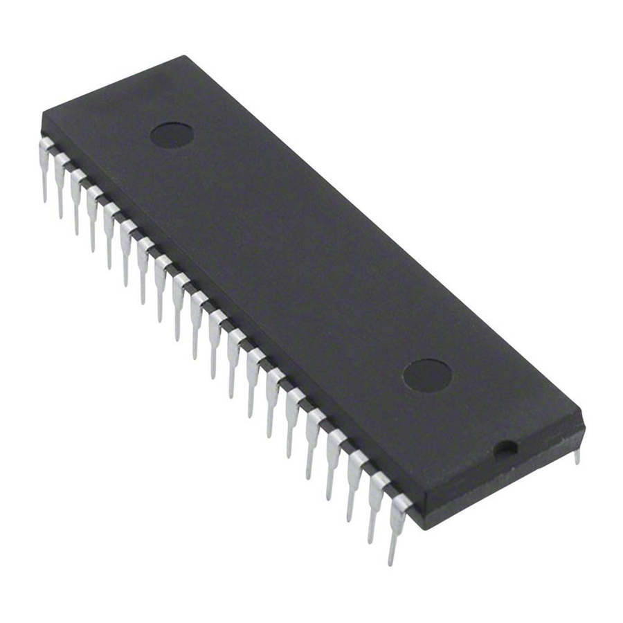
PIC16F87X
Pin Diagram
PDIP
MCLR/V
/THV
1
PP
RA0/AN0
2
RA1/AN1
3
RA2/AN2/V
-
REF
4
RA3/AN3/V
+
REF
5
RA4/T0CKI
6
RA5/AN4/SS
7
RE0/RD/AN5
8
RE1/WR/AN6
9
RE2/CS/AN7
10
V
DD
11
V
SS
12
OSC1/CLKIN
13
OSC2/CLKOUT
14
RC0/T1OSO/T1CKI
15
RC1/T1OSI/CCP2
16
RC2/CCP1
17
RC3/SCK/SCL
18
RD0/PSP0
19
RD1/PSP1
20
Peripheral Features:
• Timer0: 8-bit timer/counter with 8-bit prescaler
• Timer1: 16-bit timer/counter with prescaler,
can be incremented during sleep via external
crystal/clock
• Timer2: 8-bit timer/counter with 8-bit period
register, prescaler and postscaler
• Two Capture, Compare, PWM modules
- Capture is 16-bit, max. resolution is 12.5 ns
- Compare is 16-bit, max. resolution is 200 ns
- PWM max. resolution is 10-bit
• 10-bit multi-channel Analog-to-Digital converter
• Synchronous Serial Port (SSP) with SPI
™
2
Mode) and I
C
(Master/Slave)
• Universal Synchronous Asynchronous Receiver
Transmitter (USART/SCI) with 9-bit address
detection
• Parallel Slave Port (PSP) 8-bits wide, with
external RD, WR and CS controls (40/44-pin only)
• Brown-out detection circuitry for
Brown-out Reset (BOR)
40
RB7/PGD
RB6/PGC
39
38
RB5
37
RB4
RB3/PGM
36
RB2
35
34
RB1
33
RB0/INT
V
32
DD
31
V
SS
30
RD7/PSP7
29
RD6/PSP6
RD5/PSP5
28
RD4/PSP4
27
RC7/RX/DT
26
RC6/TX/CK
25
RC5/SDO
24
23
RC4/SDI/SDA
RD3/PSP3
22
21
RD2/PSP2
™
(Master
DS30292B-page 1
Advertisement
Table of Contents

Subscribe to Our Youtube Channel
Related Manuals for Microchip Technology PIC16F87X


Summary of Contents for Microchip Technology PIC16F87X
- Page 1 RD, WR and CS controls (40/44-pin only) - < 2 mA typical @ 5V, 4 MHz • Brown-out detection circuitry for - 20 µA typical @ 3V, 32 kHz Brown-out Reset (BOR) - < 1 µA typical standby current © 1999 Microchip Technology Inc. DS30292B-page 1...
- Page 2 RB3/PGM RA5/AN4/SS RE0/RD/AN5 RE1/WR/AN6 RB0/INT RE2/CS/AN7 PIC16F877 PIC16F874 RD7/PSP7 OSC1/CLKIN RD6/PSP6 OSC2/CLKOUT RD5/PSP5 RC0/T1OSO/T1CK1 RD4/PSP4 RC7/RX/DT RC7/RX/DT RC0/T1OSO/T1CKI RD4/PSP4 OSC2/CLKOUT RD5/PSP5 OSC1/CLKIN RD6/PSP6 PIC16F877 RD7/PSP7 PIC16F874 RE2/AN7/CS RE1/AN6/WR RB0/INT RE0/AN5/RD RA5/AN4/SS RA4/T0CKI RB3/PGM © 1999 Microchip Technology Inc. DS30292B-page 2...
- Page 3 MSSP, USART MSSP, USART Parallel Communications — — 10-bit Analog-to-Digital Module 5 input channels 8 input channels 5 input channels 8 input channels Instruction Set 35 Instructions 35 Instructions 35 Instructions 35 Instructions © 1999 Microchip Technology Inc. DS30292B-page 3...
- Page 4 • Fill out and mail in the reader response form in the back of this data sheet. • E-mail us at webmaster@microchip.com. We appreciate your assistance in making this a better document. © 1999 Microchip Technology Inc. DS30292B-page 4...
-
Page 5: Ra4/T0Cki
Generation Timer OSC1/CLKIN Brown-out OSC2/CLKOUT Reset In-Circuit Debugger Low-Voltage Programming MCLR Timer0 Timer1 Timer2 10-bit A/D Data EEPROM Synchronous USART CCP1,2 Serial Port Note 1: Higher order bits are from the STATUS register. © 1999 Microchip Technology Inc. DS30292B-page 5... -
Page 6: Ra5/An4/Ss
Debugger Low-Voltage Programming PORTE Parallel Slave Port RE0/AN5/RD RE1/AN6/WR MCLR RE2/AN7/CS Timer0 Timer1 Timer2 10-bit A/D Data EEPROM Synchronous USART CCP1,2 Serial Port Note 1: Higher order bits are from the STATUS register. © 1999 Microchip Technology Inc. DS30292B-page 6... -
Page 7: Osc1/Clkin
2: This buffer is a Schmitt Trigger input when used in serial programming mode. 3: This buffer is a Schmitt Trigger input when configured in RC oscillator mode and a CMOS input otherwise. © 1999 Microchip Technology Inc. DS30292B-page 7... -
Page 8: Osc2/Clkout
3: This buffer is a Schmitt Trigger input when configured as general purpose I/O and a TTL input when used in the Parallel Slave Port mode (for interfacing to a microprocessor bus). 4: This buffer is a Schmitt Trigger input when configured in RC oscillator mode and a CMOS input otherwise. © 1999 Microchip Technology Inc. DS30292B-page 8...
Need help?
Do you have a question about the PIC16F87X and is the answer not in the manual?
Questions and answers