Table of Contents
Advertisement
Quick Links
Advertisement
Table of Contents

Related Manuals for Renesas 38K0


Summary of Contents for Renesas 38K0
- Page 1 Data contained in this document may be changed without prior notification. MSD-M3A-8K02-UE RENESAS USB Full-Speed Microcomputers 38K0/38K2 Group Development Board M3A-8K02 Instruction Manual VER.1.0 RENESAS TECHNOLOGY CORPORATION RENESAS SOLUTIONS CORPORATION 2003.07.07...
- Page 2 (ii) use of non-flammable material or (iii) prevention against any malfunction or mishap. Notes regarding these materials These materials are intended as a reference to assist our customers in the selection of the RENESAS semiconductor product best suited to the customer’s application; they do not convey any license under any intellectual property rights, or any other rights, belonging to RENESAS TECHNOLOGY CORPORATION or a third party.
- Page 3 Revision History 38K0/38K2 Group Development Board M3A-8K02 Rev. No. Date Contents 2003/2/1 Draft version 2003/7/7 First Edition of PDF Version * Related Materials RENESAS Microcomputers: 38K0 (38K2) Group Data Sheet * Home page of RENESAS Semiconductors. http://www.renesas.com/en/usb ...
-
Page 4: Table Of Contents
- Index - Chapter 1 ............................ 1 M3A-8K02 ..........................1 Introduction ..............................2 Package Contents............................3 Top View..............................4 Top Boards G02/G03..........................5 Mounting AD Conversion Capacitors and Oscillators .................7 Power Supply ............................8 Switching Vcc Voltage (5V, 3.3V)......................9 USB Function ............................10 Keyboard Connection ...........................11 Jumper Functions..........................12 1.10 Flash Chip Reprogramming (G03) .......................13... -
Page 5: Chapter 1
Chapter M3A-8K02... -
Page 6: Introduction
Note 1: 38K0 Group devices come with the USB Function; 38K2 Group devices come with the USB function as well as the USB hub. M3A-8K02 consists of 4 boards: G01/G02/G03/G04. Each board is described in detail below. -
Page 7: Package Contents
RENESAS USB F ull-Speed Microcomputers 38K0/38K2 Group M3A-8K02 Package Contents * M3A-8K02G01 ------------------------------------------------------- 1 board * M3A-8K02G02 ------------------------------------------------------- 1 board * M3A-8K02G03 ------------------------------------------------------- 1 board * M3A-8K02G04 ------------------------------------------------------- 1 board * DC Plug ------------------------------------------------------- 1 piece * Accessories ------------------------------------------------------- 4 pcs. -
Page 8: Top View
RENESAS USB F ull-Speed Microcomputers 38K0/38K2 Group M3A-8K02 Top View Figure 1.2 shows the top view of M3A-8K02 with detailed component names. Power Boot Mode Set Remote-Wakeup Flash Mode Input & Switch Switch Test Button Switch Switch Power Gate Reset... -
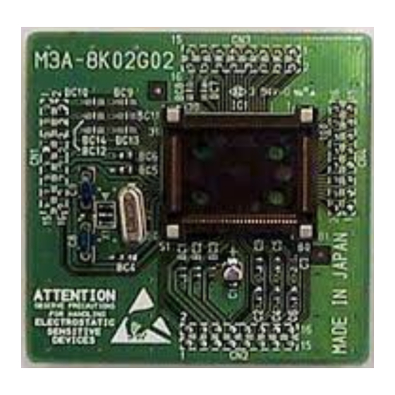
Page 9: Top Boards G02/G03
Flash chip operational verification. Because the Flash chip already contains the rewriting control program, the application software can be directly downloaded to the Flash-chip board and operational verification performed (for more details concerning Flash-chip reprogramming, see “1.11 Flash-Chip Reprogramming”). M38K29F8HPL can also run 38K0 application software. (38K2)Flash Chip Emulation Chip Socket... - Page 10 RENESAS USB F ull-Speed Microcomputers 38K0/38K2 Group M3A-8K02 Debugger Cable Emulation Chip Figure 1.3(2) G02 and Debugger Connection...
-
Page 11: Mounting Ad Conversion Capacitors And Oscillators
M3A-8K02 Mounting AD Conversion Capacitors and Oscillators The capacitor pattern for 38K0/38K2 AD conversion is located on the upper left side of both G02 and G03 (1). To evaluate AD conversion, mount 0.1uF chip capacitors (size “1608”) here. The 38K0/38K2 oscillator sockets are located on the left side of both G02 and G03 (2). Insert the bundled oscillator (6MHz or 12MHz, as required) , and a 30pF oscillator capacitor. -
Page 12: Power Supply
RENESAS USB F ull-Speed Microcomputers 38K0/38K2 Group M3A-8K02 Power Supply M3A-8K02 can run on either self-power (external supply of 5V) or bus-power (VBUS power from USB up-port). * Self-Power To run M3A-8K02 on self-power, connect the external supply through TP1 (1) or the DC jack (2), as shown in Figure 1.5. -
Page 13: Switching Vcc Voltage (5V, 3.3V)
M3A-8K02 has two power lines: 5V and Vcc. The 5V line depends on the operating voltage of the board and the Vcc line depends on the 38K0/38K2 operating voltage. The user must switch the Vcc line between 5V and 3.3V, according to the 38K0/38K2 operating voltage. Select the voltage value with the VCC SELECT Switch (S7 in 1) as shown in Fig. -
Page 14: Usb Function
This board comes with one USB up-port (1) and two USB down-ports (2). Please review the usage conditions described below before setting each port. To enable detection of the self-power mode (external power supply) on 38K0/38K2, insert a header link to the Power INT jumper (3). The detection signal is assigned to port P50/INT0. -
Page 15: Keyboard Connection
RENESAS USB F ull-Speed Microcomputers 38K0/38K2 Group M3A-8K02 Keyboard Connection M3A-8K02 has a built-in keyboard connector. Pins P00-P07, P10-P13, P24-P27, P30-P37, and P53-P57 are assigned to the keyboard connection. Figure 1.8 shows the pin configuration for the connector. USB hub keyboard firmware is available separately. -
Page 16: Jumper Functions
RENESAS USB F ull-Speed Microcomputers 38K0/38K2 Group M3A-8K02 Jumper Functions As described previously, the jumpers equipped on this board can be set for specific functions. Table 1.9 shows the jumper number and corresponding function. Table 1.9 Jumper Number and Function JP No. -
Page 17: Flash Chip Reprogramming (G03)
(S10 in 2) Table 1.10 shows the setup conditions for the BOOT-MODE switch. By setting the FLASH switch (S9 in 1) to ON and supplying power to the board (Note 2), the FLASH lamp (LED5 in 3) will go on and 38K0/38K2 will be in the Flash reprogramming mode. -
Page 18: Serial Reprogramming (Flash Writer)
1.10.1 Serial Reprogramming (Flash Writer) The M3A-8K02 board allows the user to reprogram the 38K0/38K2 Flash chip on board (serial reprogramming of F/W) using a flash writer. To perform serial reprogramming, insert the flash writer cable in the flash writer connecter (1), set the VCC-SELECT switch (S7) to 5V, the BOOT-MODE switch (S10 in 2) to P42 = “H”... -
Page 19: Flash Over Usb Reprogramming (Fousb)
The FLASH lamp (4) will go on and the host will recognize operations with “RENESAS Flash-Over USB.” After the host PC is connected, run the application program bundled with the M3A-8K02 on the PC and follow the instructions for reprogramming the application firmware. -
Page 20: Peripheral Circuits
G01 will be supplied to Vcc pins TP10, TP11, TP12, and TP13. * System RESET Pin The main board RESET signal can be used for the external universal board as well. To reset external circuits in the same manner as 38K0/38K2, use RESET pin TP8 (5). 3. PowerGate 4. Power Switch 2. - Page 21 RENESAS USB F ull-Speed Microcomputers 38K0/38K2 Group M3A-8K02 RESET Figure 1.11(2) Board Pin Numbers ...
-
Page 22: Components Table
RENESAS USB F ull-Speed Microcomputers 38K0/38K2 Group M3A-8K02 1.12 Components Table Table 1.12 shows the various components of the M3A-8K02 main board G01 (the same information applies to G02, G03, and G04). Note that the components listed here are not guaranteed for operation in the users’... - Page 23 RENESAS USB F ull-Speed Microcomputers 38K0/38K2 Group M3A-8K02 Component Name Spec. Component No. Notes Name Symbol (Schematic No., Maker Prod. Spec.) TP28, TP31, TP34, P20-P27 TP26, TP29, TP32, TP35, HK-5-G orange MAC8 Surface mount (orange) P30-P37 TP7, TP11, TP15, HK-5-G yellow...
-
Page 24: Chapter 2
Chapter Other Development Boards... -
Page 25: G02,G03,G04 Options
M3A-8K02G02, M3A-8K02G03, or M3A-8K02G04. Figure 2.1 G02, G03, G04 Options M3A-8K10 (COM Class Demo Board) M3A-8K10G01, a COM Class demonstration board, is also available for the 38K0 Group. Please contact your local representative for more details. Figure 2.2 COM Class Demo Board M3A-8K10G01... -
Page 26: M38C29T-64Fpd
RENESAS USB F ull-Speed Microcomputers 38K0/38K2 Group M3A-8K02 M38C29T-64FPD M38C29T-64FPD is a package conversion board for connecting the emulation chip to the HP package foot pattern (64P6Q-A). Use this board when the emulation chip 100-pin socket (100P6S_A) foot pattern does not fit the trial board. -
Page 27: Chapter 3
Chapter Development Environment... -
Page 28: Development Environment Example
RENESAS USB F ull-Speed Microcomputers 38K0/38K2 Group M3A-8K02 Development Environment Example Table 3.1 shows the types of tools required for the firmware development environment of the M38K0/38K2 Group. Table 3.1 Development Environment Example Product Number Host Machine PC/AT compatible (with LPT parallel, USB interface) - Page 29 RENESAS USB Full-Speed Microcomputer 38K0/38K2 Group Development Board M3A-8K02 Instruction Manual VER.1.0 RENESAS TECHNOLOGY CORPORATION. RENESAS SOLUTIONS CORPORATION. No unauthorized copy, please. Any contents (including charts) are not allowed for reprinting without contact to RTC. Copyright(C) 2003 RENESAS TECHNOLOGY CORPORATION and RENESAS SOLUTIONS CORPORATION.
- Page 30 WakeUp SW TP16 220uF 0.1uF P52 WakeUp BLM21PG221SN1D OvCur DP1 OvCur DP2 USB DP2 VBUS M3A-8K02G01 TC7SH08FU RENESAS SOLUTIONS Corp. + C3 BLM21PG221SN1D 220uF 0.1uF OverCurrent INT Title M3A-8K02 G01 Size Document Number DW30146 (1/3) Date: Monday, September 29, 2003...
- Page 31 RESET To FLASH BOOT-MODE BC10 IC11 MAX394CWP 0.1uF 100k CNVss To COM1 COM2 COM3 LED5 COM4 LED6 LED7 LED8 LED9 FLASH SERIAL M3A-8K02G01 RENESAS SOLUTIONS Corp. Title M3A-8K02 G01 Size Document Number DW30146 (2/3) Date: Monday, September 29, 2003 Sheet...
- Page 32 P23/D2+ P43/ExA1/SRDY P42/ExTC/SCLK P41/ExDACK/TxD P40/ExDREQ/RxD P07/KI7 P06/KI6 CN10 Keyboard Scan TP24 TP25 TP26 TP27 TP28 TP29 TP30 TP31 TP32 TP33 TP34 TP35 M3A-8K02G01 RENESAS SOLUTIONS Corp. Title M3A-8K02 G01 Size Document Number DW30146 (3/3) Date: Monday, September 29, 2003 Sheet...
- Page 33 P13/DQ3/AN3 P12/DQ2/AN2 P17/DQ7/AN7 P16/DQ6/AN6 P15/DQ5/AN5 P14/DQ4/AN4 P13/DQ3/AN3 P12/DQ2/AN2 P11/DQ1/AN1 P10/DQ0/AN0 M3A-8K02G02 BC10 BC11 BC12 BC13 BC14 RENESAS SOLUTIONS Corp. **0.1uF **0.1uF **0.1uF **0.1uF **0.1uF **0.1uF **0.1uF **0.1uF Title M3A-8K02 G02 Size Document Number DW30147 **= Pattern only Date: Monday, September 29, 2003...
- Page 34 P21/D1+ P21/D1+ P07/KI7 P07/KI7 0.1uF 2.2uF P06/KI6 P22/D2- P06/KI6 P22/D2- P06/KI6 P22/D2- P06/KI6 P23/D2+ P23/D2+ P23/D2+ M3A-8K02G03 RENESAS SOLUTIONS Corp. P20/D1- P21/D1+ P22/D2- P23/D2+ Title M3A-8K02 G03 Size Document Number 68pF 68pF 68pF 68pF 68pF 68pF DW30148 **= Pattern only...
- Page 35 TP11 TP12 TP13 5V IN FY4DJ-03A TP14 TP15 TP16 TP17 TP18 POWER GND **10uF 100k LED1 POWER SW HEADER 32X2 M3A-8K02G04 RENESAS SOLUTIONS Corp. Title M3A-8K02 G04 Size Document Number DW30149 **= Pattern only Date: Monday, September 29, 2003 Sheet...
Need help?
Do you have a question about the 38K0 and is the answer not in the manual?
Questions and answers