Table of Contents
Advertisement
Quick Links
Contents
TLE9879 EvalKit V1.4 User Manual .................................................................................................... 1
1
Abbreviations ........................................................................................................................ 2
2
Concept ................................................................................................................................ 3
3
Interconnects ........................................................................................................................ 4
4
Test Points ............................................................................................................................ 6
5
Jumper Settings ..................................................................................................................... 7
6
Communication Interfaces ...................................................................................................... 9
6.1
LIN (via Banana jack and uIO BSL) .......................................................................................................... 9
6.2
UART (via USB)......................................................................................................................................... 9
6.3
Debugging (via USB or SWD-Interface) ................................................................................................... 9
7
Technical Data ...................................................................................................................... 10
8
Optional Additional Placements.............................................................................................. 11
9
Changes with v1.3: Schematic ................................................................................................ 12
10
Schematics and Layout .......................................................................................................... 13
10.1
Schematic .............................................................................................................................................. 13
10.2
Layout .................................................................................................................................................... 17
TLE9879 EvalKit V1.4 User Manual
TLE9879 EvalKit V1.4 User Manual
1
Advertisement
Table of Contents

Related Manuals for Infineon TLE9879 EvalKit V1.4


Summary of Contents for Infineon TLE9879 EvalKit V1.4
-
Page 1: Table Of Contents
TLE9879 EvalKit V1.4 User Manual Contents TLE9879 EvalKit V1.4 User Manual ....................1 Abbreviations ........................2 Concept ..........................3 Interconnects ........................4 Test Points ..........................6 Jumper Settings ........................7 Communication Interfaces ...................... 9 LIN (via Banana jack and uIO BSL) ......................9 UART (via USB)............................ -
Page 2: Abbreviations
VCOM Virtual COM-Port Voltage Charge Pump VDDC Core Supply VDDEXT External Voltage Supply Output VDDP I/O Port Supply Voltage Drain High side MOSFET Battery Supply Input Battery Supply Input for MOSFET Driver Table 1: Abbreviations TLE9879 EvalKit V1.4 User Manual... -
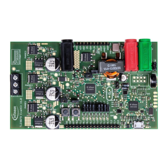
Page 3: Concept
Concept Figure 1: Board Concept This board provides a simple, easy-to-use tool for getting familiar with Infineon’s Embedded Power IC TLE9879QXA40 (further to be named: TLE9879). It contains the TLE9879 and its typical application circuit including three MOSFET half bridges to drive a BLDC motor. The board is ready to connect with car supply or similar and has an onboard J-Link debugger. -
Page 4: Interconnects
The three pins of the terminal block provide access to the three half bridges and are intended to connect a DC brushless motor. USB for UART and Debugging (marked green) With this Micro USB PC and evaluation board can get connected. TLE9879 EvalKit V1.4 User Manual... - Page 5 For the uIO bootstrap loader an 8 pin header (2 x 4) with 2.54 mm pitch is placed on the board. It is intended to connect additional hardware for bootstrap loading. This uIO interface can be used to program the TLE9879 via LIN (see www.infineon.com/uio). RESET...
-
Page 6: Test Points
Additionally, there is an intended test point for VDDC and various ground points. All test points marked in the following figure are not populated. In order to use these pins, they have to be soldered in the designated solder holes. TLE9879 EvalKit V1.4 User Manual... -
Page 7: Jumper Settings
Connect or disconnect VAREF with VDDEXT Replace by an ampere meter to measure input current Enable or disable POTI Enable or disable LED for respective GPIO Table 6: Jumpers’ functionalities JP1 JP2 Figure 4: Jumpers TLE9879 EvalKit V1.4 User Manual... - Page 8 JP7: Jumper 7 provides one individual jumper per LED in order to connect or disconnect the respective LED to the pin port. P0.1 P0.2 P0.3 P1.2 P1.0 P1.3 P1.4 P0.4 LED1 LED2 LED3 LED4 LED5 LED6 LED7 LED8 Table 7: Combinations of GPIOs and LEDs TLE9879 EvalKit V1.4 User Manual...
-
Page 9: Communication Interfaces
SWD interface between the XMC4200 and the TLE9879. The pin configuration makes sure that the XMC is hold in reset while another debugger is physically connected as DBPRE will be implicitly connected to GND by connecting the external ISP (see Table 5). TLE9879 EvalKit V1.4 User Manual... -
Page 10: Technical Data
Technical Data Platine Size 110x66 mm Voltage supply max. 28V Motor current max. 20 A Pin ports 5 V (GPIOs of TLE9879) Table 8: Technical Data TLE9879 EvalKit V1.4 User Manual... -
Page 11: Optional Additional Placements
Capacitor Snubber High side MOSFET Phase 3 Gate Drain Capacitor High side MOSFET Phase 3 Resistance Snubber Low side MOSFET Phase 3 Capacitor Snubber Low side MOSFET Phase 3 Gate Drain Capacitor Low side MOSFET Phase 3 Table 8: Additional Placements TLE9879 EvalKit V1.4 User Manual... -
Page 12: Changes With V1.3: Schematic
Changes with v1.3: Schematic Pin P2.0 and pin P2.2 were swapped in the schematic. TLE9879 EvalKit V1.4 User Manual... -
Page 13: Schematics And Layout
Schematics and Layout 10.1 Schematic TLE9879 EvalKit V1.4 User Manual... - Page 14 TLE9879 EvalKit V1.4 User Manual...
- Page 15 TLE9879 EvalKit V1.4 User Manual...
- Page 16 TLE9879 EvalKit V1.4 User Manual...
-
Page 17: Layout
10.2 Layout Top Layer Layer 2 TLE9879 EvalKit V1.4 User Manual... - Page 18 Layer 3 Bottom Layer TLE9879 EvalKit V1.4 User Manual...
Need help?
Do you have a question about the TLE9879 EvalKit V1.4 and is the answer not in the manual?
Questions and answers