Table of Contents
Advertisement
Quick Links
Advertisement
Table of Contents

Related Manuals for Terasic ADC-FMC


Summary of Contents for Terasic ADC-FMC
-
Page 2: Table Of Contents
TABLE OF CONTENTS Chapter 1 Introduction ........................2 1.1 The Package Contents ..........................2 1.2 Assemble ADC-FMC with FPGA Mainboard .................... 3 1.3 Connectivity ............................... 4 1.4 Getting Help ............................... 5 Chapter 2 Architecture of ADC-FMC ....................6 2.1 Features............................... 6 2.2 Component and Layout .......................... -
Page 3: Chapter 1 Introduction
Chapter 1 Introduction The Terasic ADC-FMC is a four-channel high speed ADC daughter card with FMC interfaced. Two AD9648BCPZ-125 chips are used in this board. One AD9648BCPZ-125 chip can provide two ADC channels, and each channel can provide maximal 125 MSPS with 14-bits resolution data. The build-in onboard clock generator (Si5340B) provides the reference clock for the ADC chip. -
Page 4: Assemble Adc-Fmc With Fpga Mainboard
In order to make the ADC-FMC daughter card and the FMC connector on the FPGA mainboard with more secure hookup, the FMC side of the ADC-FMC daughter card has reserved two screw holes, as shown in Figure 1-2. Users can use the screws, copper pillars, and nuts that come with the... -
Page 5: Connectivity
1-5 below show the connectivity of the ADC-FMC to the TR5 and A5SoC FPGA boards. The ADC-FMC is powered from FPGA mainboard. It is not necessary to connect a power adapter to the ADC-FMC. There are four ADC channels on the ADC-FMC board. -
Page 6: Getting Help
Figure 1-5 ADC-FMC with A5SoC For Technical Support, Terasic’s Contact Information is listed below: ⚫ Office Hours: 9:00 a.m. to 6:00 p.m. (GMT +8) ⚫ Telephone: +886-3-575-0880 ⚫ Email: support@terasic.com ADC-FMC User Manual www.terasic.com April 24, 2020... -
Page 7: Architecture Of Adc-Fmc
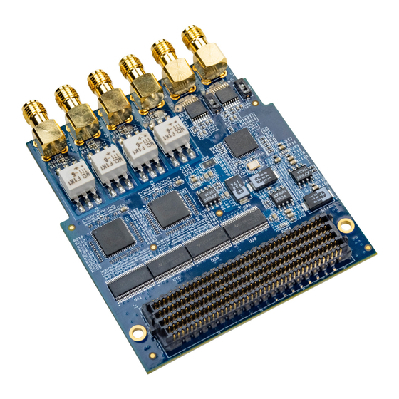
Chapter 2 Architecture of ADC-FMC This chapter lists the features and describes the architecture of ADC-FMC daughter card. There are four ADC channels on the board. Two channels utilize the low pin count of the FMC connector, and the other two channels utilized the high pin count of the FMC connector. To use four ADC channels, the mainboard’s FMC connect must support 1.8V full pin count. - Page 8 Figure 2-1 Top view of the ADC-FMC Daughter Card The bottom view of the ADC-FMC is shown in Figure 2-2. It depicts the layout and indicates the locations of connectors and key components. Figure 2-2 Bottom view of the ADC-FMC Daughter Card ADC-FMC User Manual www.terasic.com...
-
Page 9: 2.3 Block Diagram
2.3 Block Diagram Figure 2-3 shows the block diagrams of the ADC-FMC. Two AD9648BCPZ-125 chips are used in this board. One AD9648BCPZ-125 chip can provide two ADC channels, and each channel can provide maximal 125 MSPS with 14-bits resolution data. The four analog inputs come from the on-board SMA connector. -
Page 10: Using The Adc-Fmc
Chapter 3 Using the ADC-FMC This chapter provides information on how to control the hardware of the ADC-FMC. It includes the definition of the FMC interface and how to use the ADC chips and clock generator hardware in the board. - Page 11 Figure 3-2 Signal names of FMC connector part 2 Figure 3-3 Signal names of FMC connector part 3 Table 3-1 shows the ADC-FMC pin assignments for the ADC-FMC pins in Quartus Prime. Table 3-1 ADC-FMC Pin Assignments of FMC in Quartus Prime Signal Name Description Pin No.
- Page 12 Second ADC Port-A Data0 input VCCADJ ADC_C_D1 Second ADC Port-A Data1 input VCCADJ ADC_C_D2 Second ADC Port-A Data2 input VCCADJ ADC_C_D3 Second ADC Port-A Data3 input VCCADJ ADC_C_D4 Second ADC Port-A Data4 input VCCADJ ADC-FMC User Manual www.terasic.com April 24, 2020...
- Page 13 (Active Low) Second ADC Output Enable ADC2_OEB output VCCADJ (Active Low) ADC2_SYNC Second ADC Digital output VCCADJ Synchronization ADC2_CK_S0 Second ADC Clock Selection output VCCADJ bit0 ADC2_CK_S1 Second ADC Clock Selection output VCCADJ bit1 ADC-FMC User Manual www.terasic.com April 24, 2020...
-
Page 14: Using The Adc Chip Ad9648Bcpz-125
The ADC chip can be configured via its SPI interface. The default ADC sampling rate is equal to the frequency of the reference clock CLK+/CLK-. Developers can modify the DIVIDE register to change the ratio between reference clock frequency and sampling rate. ADC-FMC User Manual www.terasic.com April 24, 2020... -
Page 15: Select Reference Clock Source For Adc
ADC chip, and OUT1 provides reference clock for the second ADC chip. Developers can modify the output frequency by configure Si5340B via its I2C interface. If SMA clock source is selected, developers need to provide clock source via SMA connector. ADC-FMC User Manual www.terasic.com April 24, 2020... - Page 16 When switches are off, the input clock voltage is expected to 3.3V. When switches are on, the input clock voltage is expected to 2.5V. If FPGA clock source is selected, developers need to provide difference clock source to FPGA_CLK_ADC1_p/n and FPGA_CLK_ADC2_p/n. ADC-FMC User Manual www.terasic.com April 24, 2020...
-
Page 17: Chapter 4 Adc Demonstrations
FIFO and selected as sampling clock in Signal Tap Logic Analyzer. The output data of each FIFO is selected as sampling data in Signal Tap Logic Analyzer. Figure 4-1 Block Diagram of Demonstration ADC-FMC User Manual www.terasic.com April 24, 2020... -
Page 18: Demo On Tr5 Fpga Mainboard
This section shows how to setup the demo on the Terasic TR5 FPGA Board. TR5 FMC-A connector is used to connect the ADC-FMC board in this demo. User also can use FMC-D connector on TR5. FMC-B and FMC-C on TR5 are not recommended because they are low pin count FPGA connectors, only two ADC channels can be used. - Page 19 ADC2_CLK on ADC-FMC card to CLK_OUT_n (J2) on TR5 board. Set the SW1/SW2 on ADC-FMC card as ON. b) External 125MHz clock generator: Set the SW1/SW2 on ADC-FMC card as OFF if the clock generator output signal is 3.3V standard, or set SW1/SW2 as ON if the output signal is 2.5V.
-
Page 20: Demo On Intel A5Soc Fpga Mainboard
This section shows how to setup the demo on the Intel A5SoC FPGA Board. A5SoC FMC-A connector is used to connect the ADC-FMC board in this demo. User also can use FMC-B connector on A5SoC. Both FMC connectors on A5SoC are low pin count, so only two ADC channels can be used. - Page 21 Connect ADC1_CLK and ADC2_CLK on ADC-FMC card to external 125MHz clock generator through two SMA cables. Set the SW1/SW2 on ADC-FMC card as OFF if the clock generator output signal is 3.3V standard, or set SW1/SW2 as ON if the output signal is 2.5V.
- Page 22 Figure 4-8 SWITCH[1:0] on A5SoC ◼ Project Source Code The source code of Quartus project for the ADC demo with the A5SoC board is available in the “Demonstrations\A5SoC_ADC-FMCA” folder from the ADC-FMC System CD. ADC-FMC User Manual www.terasic.com April 24, 2020...
-
Page 23: Chapter 5 Appendix
Change Log V1.0 10/24, 2018 Initial Version (Preliminary) V1.1 07/18, 2019 Update for rev B (Adding buffer) V1.2 04/24, 2020 Modify Figure 3-1,3-2,3-3 and Table 3-1 Copyright © Terasic Inc. All rights reserved. ADC-FMC User Manual www.terasic.com April 24, 2020...
Need help?
Do you have a question about the ADC-FMC and is the answer not in the manual?
Questions and answers