Advertisement
800/900MHz DIGITAL TRANSCEIVER
RA070<Rev.001>
B5B-7311-00
3 S ERVICE MANUAL
2019
COPYRIGHT © 2019 JVC KENWOOD Corporation
1
PRECAUTION. . . . . . . . . . . . . . . . . . . . . . . . . . . . . . . . . . . . . . . . . . . . . . . . . . . . . . . . . . . . . . . . . . . . . . . . . 1-4
2
SPECIFIC SERVICE INSTRUCTIONS . . . . . . . . . . . . . . . . . . . . . . . . . . . . . . . . . . . . . . . . . . . . . . . . . . . . . . 1-4
3
DISASSEMBLY . . . . . . . . . . . . . . . . . . . . . . . . . . . . . . . . . . . . . . . . . . . . . . . . . . . . . . . . . . . . . . . . . . . . . . 1-24
4
ADJUSTMENT . . . . . . . . . . . . . . . . . . . . . . . . . . . . . . . . . . . . . . . . . . . . . . . . . . . . . . . . . . . . . . . . . . . . . . . 1-29
5
TROUBLESHOOTING . . . . . . . . . . . . . . . . . . . . . . . . . . . . . . . . . . . . . . . . . . . . . . . . . . . . . . . . . . . . . . . . . 1-57
This product complies with the RoHS directive for the European market.
B5B-7311-00
SERVICE MANUAL
COPYRIGHT © 2019 JVC KENWOOD Corporation
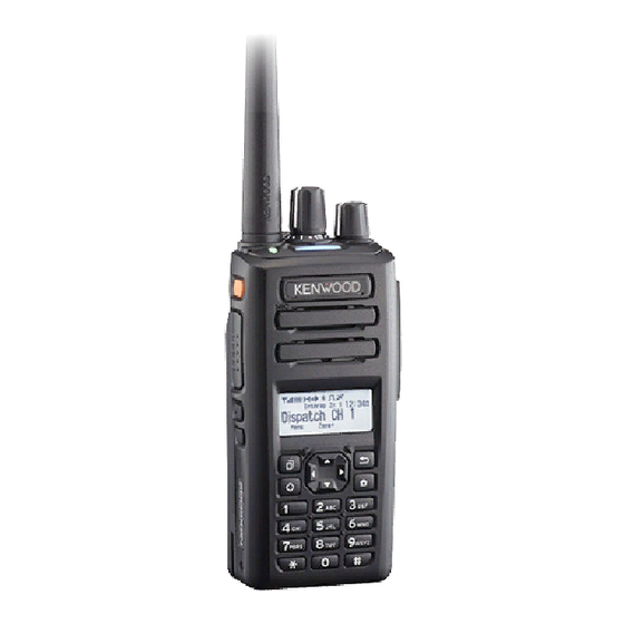
NX-3400
TABLE OF CONTENTS
This product uses Lead Free solder.
No.RA070<Rev.001>
2019/3
Advertisement

Related Manuals for Kenwood NX-3400


Summary of Contents for Kenwood NX-3400
-
Page 1: Table Of Contents
B5B-7311-00 NX-3400 COPYRIGHT © 2019 JVC KENWOOD Corporation TABLE OF CONTENTS PRECAUTION............... . . 1-4 SPECIFIC SERVICE INSTRUCTIONS . - Page 2 Neither is any liability assumed for damages resulting from the use of the information contained herein. JVC KENWOOD Corporation reserves the right to make changes to any products herein at any time for improvement purposes. Firmware Copyrights The title to and ownership of copyrights for firmware embedded in KENWOOD product memories are reserved for JVC KENWOOD Corporation.
- Page 3 Analog measurements made per TIA603. Specifications are measured according to applicable standards. Battery Life is measured by Battery Save ON, GPS/Bluetooth OFF, 3 W for 800/900MHz Bands. JVC KENWOOD Corporation reserves the right to change specifications without prior notice or obligation. (No.RA070<Rev.001>)1-3...
-
Page 4: Precaution
This service manual does not describe PRECAUTION. SECTION 2 SPECIFIC SERVICE INSTRUCTIONS SYSTEM SET-UP Type Frequency range (MHz) RF power Merchandise received DTMF keypad NX-3400 K3 806~825 851~870 896~902 935~941 Choose the type of transceiver 851~870 935~941 A personal computer, programming interface (KPG-36U/36X), and FPU (programming software) are required for programming. - Page 5 REALIGNMENT 2.2.2 How to Enter Each Mode 2.2.1 Modes Mode Operation User mode Power ON User mode Panel test mode*2 • [ ] + Power ON Panel tuning mode Panel test mode • [ ] + Power ON Select the “Panel Test” using the [] / [] button.
- Page 6 (KPG-36U/36X). (Connection is same as in the PC mode.) 2.2.6.3 Programming (1) Start up the firmware programming software (KENWOOD Firmware Loader). The KFL.exe exists in the KPG-D3/D3N installed folder. (2) Set the baud rate to "auto" or 1152000, 576000, 115200, and 57600.
- Page 7 2.2.7 Clone Mode (7) The other target can be continuously cloned. When the Programming data can be transferred from one transceiver to ] button on the source is pressed while the source another by connecting them via their external universal displays “END”, the source displays “CLONE MODE”.
- Page 8 2.2.8.2 Data Writing Setup item Display Remarks Before moving to next Zone/Channel, “Keep This Change?” 7 TX Signaling TX QT/DQT Transmit QT/DQT appears on the LCD, if you select “OK”, the new data is written to memory. If you select “Cancel”, the new data not be written; 8 RX RAN RX RAN None, 1~63...
- Page 9 Button operation (2/3) Button\ RX Signaling TX Signaling RX RAN TX RAN Color Code Slot Selection Transmit Item Power Decision Decision Decision Decision Decision Decision Decision Back to the Back to the Back to the Back to the Back to the Back to the Back to the previous item...
- Page 10 Front panel programming mode flow chart Input Password Enter the Front panel programming mode Clone/Front Panel Password by using section "2.2.2 How to Enter Each Mode". Front panel Programming mode ] or [ Keep This Change? Zone Select Channel Name Channel Select ] or [ Transmit Power...
- Page 11 2.3.1 Overview The NX-3400 is 800/900MHz Dual Band Analog FM & Digital Portable transceiver designed to operate in the frequency range of 806 to 870MHz and 896 to 941MHz. The unit consists of a transceiver IC, a transmitter, a digital control unit, and a power supply circuit.
- Page 12 2.3.3 Receiver System 2.3.3.1 RF Circuit The receive signal from ANT SW (D201, D202, D203 and D207) passes through the high-pass filter (L302, L307, L308, L312, L314 and L315) to remove unwanted signals and amplified by a RF amplifier (incorporated in Transceiver IC (IC303)). The signal is then fed to the mixer (incorporated in Transceiver IC (IC303)) and converted to the baseband signal.
- Page 13 2.3.4 Transmitter System 2.3.4.1 Audio Band Circuit The signal from microphone is amplified and converted to digital signal by IC601, IC601 includes AGC function. Digital signal is transferred to MPU/DSP (IC401). 2.3.4.2 Baseband Circuit The audio signal transferred from CODEC (IC601) is processed at MPU/DSP (IC401). Voice signals of 300Hz or lower and frequencies of 3kHz or higher are cut off and an audio range 300Hz to 3kHz is extracted.
- Page 14 2.3.5.2 There are two VCO contain VCO_L for 800MHz and VCO_H for 900MHz. The VCO_H (Q131) generates the carrier for the transmitter (Frequency range: 896 to 941MHz) and the receiver (Frequency range: 935 to 941MHz). VCO oscillation frequency range is 1792 to 1882MHz. The VCO_L (Q151) generates the carrier for the transmitter (Frequency range: 806 to 870MHz) and the receiver (Frequency range: 851 to 870MHz).
- Page 15 2.3.6.5 Low Battery Warning The battery voltage is divided using R65 and R66, it is detected by A/D converter (IC409). When the battery voltage falls below the voltage set by the Low battery warning adjustment, the red LED blinks to notify the operator that it is time to replace the battery. If the battery voltage falls even more (approx.
- Page 16 (3.15A) Battery Final Amp, APC IC10 MPU/DSP RTC 31BU 12BU BackUp Battery MPU/DSP Core, MPU/DSP PLL, CODEC VDD MPU/DSP 1.8V I/O, mobile DDR, LCD Module I/O IC12 Flash Memory I/O 18M_3 BT & GPS I/O 18BT BT & GPS VDD 32BT IC11 CODEC VDD,...
- Page 17 IC17 KEY Back Light, 3Color LED, 8bit/16ch ADC IC602 Universal Option IC201 ANT SW ANT SW IC15 TX circuit 8bit ADC (0.5A) Int AF Amp 53AF Ext AF Amp Fig.6 Power supply circuit 2.3.8 Signaling Circuit 2.3.8.1 Encode (QT/DQT/LTR/DTMF/MSK) Each signaling data signal of QT, DQT, LTR, DTMF and MSK is generated by MPU/DSP (IC401), superposed on a modulation signal and output to VCO and PLL.
- Page 18 2.3.9.1 Bluetooth Circuit The Bluetooth/GPS IC (IC351) support Bluetooth 4.0 up to HCI level. Basic Rate TX/RX frequency is 2400-2483.5MHz (79ch Hopping, 2402-2480MHz, 1MHz step). Transmitting power is +0dBm (Max.: +4dBm) at Bluetooth antenna input. Low Energy TX/RX frequency is 2400-2483.5MHz (40ch (3 advertising channels: Single carrier, 37data channels: Hopping), 2402-2480MHz, 2MHz step).
- Page 19 COMPONENTS DESCRIPTION Ref. No. Part Name Use / Function 2.4.1 MAIN unit (XC1-276K-00) Transistor DC switch (Codec IC) Ref. No. Part Name Use / Function Q102 DC switch (Assist) Voltage detector Q103 DC switch DC/DC converter (12M) Q111 DC switch (VCO) DC/DC converter (38M) Q112 DC switch...
- Page 20 Ref. No. Part Name Use / Function Pin No. Name Function D601 Diode Reverse current protection - No connection D609 Diode Reverse current protection CN402 D620,621 Zener diode Over voltage protection 32LCD O DC 3.2V output D622,623 Diode Over voltage protection 32LCD O DC 3.2V output D624-628...
- Page 21 Pin No. Name Function Pin No. Name Function CN625 VB0- - LCD bias voltage. Connect to VB0+ via a capacitor. SMIC I External MIC input VLCD O Main LCD power supply RXD/USB_DM I/O Serial data input / USB DM CN202 TXD/USB_DP I/O Serial data output / USB DP - GND...
- Page 22 2.5.3 DISPLAY unit (XC1-209K-02 B/2) Pin No. Name Function CN301 I Emergency input - GND SIDE2 I Side 2 input SIDE1 I Side 1 input I PTT input - No connection 2.5.4 14Pin Universal Connector Specification Rating and Condition Signal Pin Name Description Type...
- Page 23 Rating and Condition Signal Pin Name Description Type Parameter Unit - Power 5V power supply output Output Voltage (Iout = 100mA) Maximum Current O Digital Serial data output VOH(Io=-5mA) CMOS VOL(Io=5mA) Baud Rate 1.1875 Mbps USB_DP I/O Analog USB DP Baud Rate Mbps (Full-Speed)
-
Page 24: Disassembly
SECTION 3 DISASSEMBLY Precautions for Waterproof • Do not remove the black sheet from the reverse side of the transceiver (refer to the illustration below). Removal of this sheet decreases the waterproof efficiency of the transceiver and may cause malfunctions if water seeps into the transceiver. •... - Page 25 • When the chassis cannot be removed from the front case, remove by pushing in the button top with the finger. • Regarding VOID, confirm the service policy of the NX- 3400 to KENWOOD (or authorized distributor). VOID seal <3> <3>...
- Page 26 3.2.6 Removing the MAIN unit from the chassis 3.2.7 Removing the TOP packing (1) Remove the following parts in numerical order. (1) Pull the TOP packing to the left to remove the packing that <1>VOL/SEL FPC <2>PTT FPC <3>Universal FPC is fit into the left groove of the chassis.
- Page 27 3.2.8 Removing the TERMINAL BLOCK (with PACKING) Circular nut <2> (1) Remove the screw. <1> <1> (2) Remove the TERMINAL BLOCK (with PACKING). <2> <1> TERMINAL BLOCK Note: <2> When reassembling, make sure the stopper and the circular nut are engaged. 3.2.10 Removing the LCD from the Display unit (1) Remove the LCD FPC from the connector.
- Page 28 CUSHION (AIR LEAK) G1D-0204-00 SHEET (AIR LEAK) G11-4440-04 SHEET (PTT) G1G-0075-00 ADHESIVE SHEET (UNIV CN) J99-0715-08 CABINET ASSY (FULL) A0C-0176-30 STICKER (NEXEDGE) B42-7417-04 KENWOOD BADGE B4D-0044-10 FIBROUS SHEET G1A-0053-00 HOLDER J1K-0493-10 FIBROUS SHEET (MIC) G1A-0057-00 CUSHION (SP) G1D-0203-10 SHEET (BUTTON) G1G-0076-00...
-
Page 29: Adjustment
SECTION 4 ADJUSTMENT Controls Selector knob Power switch/ Volume control Transmit/ Receive/ Battery low indicator Light Bar Auxiliary (orange) button PTT (Push-To-Talk) switch Side 1 button 4-way D-pad Side 2 button 4.1.1 Preparations for checking/tuning the transceiver 4.2.2 Button operation Before attempting to check/tune the transceiver, connect the unit Function OFF: "Func"... - Page 30 Function ON: "Func" appears on the sub LCD display Button Function Display [Selector] [] Talk Around On/Off On: [ ] icon appears [] Analog/NXDN/DMR Analog: "A" NXDN: "N" DMR: "D" [] Function off [] Button/LCD check The position of the selector knob, etc., appear.
- Page 31 4.2.3 Frequency and Signaling NXDN Type Signaling The transceiver has been adjusted for the frequencies shown in the following table. When required, readjust them following the RAN1 RAN1 adjustment procedure to obtain the frequencies you want in actual operation. None (1) Test frequency RAN1...
- Page 32 Panel Tuning Mode 4.3.2 Button operation 4.3.1 Transceiver tuning (To enter tuning mode) Button Function To enter tuning mode, press the [ ] button while the transceiver Push Hold (1 second) is in test mode. Use the [ ] button to write tuning data through tuning modes, and the [ ...
- Page 33 10 reference level adjustment (Analog Narrow, NXDN Narrow, NXDN Very Narrow, DMR) VCO Assist / High Transmit Power / Low Transmit Power / Balance / Maximum Deviation / NXDN High Deviation / DMR High Deviation / QT Deviation / DQT Deviation / LTR Deviation / DTMF Deviation / MSK Deviation / CW ID Deviation <10 points>...
- Page 34 4.3.5 Adjustment item and Display Order Adjustment Main Sub LCD Adjust item display (Analog (Analog (Analog (NXDN (NXDN Very (DMR) item display Wide 5k) Wide 4k) Narrow) Narrow) Narrow) Number Adjustment range LCD Contrast CNTR 1 point ADJ Common Section 2 1~256 VCO Assist (CV voltage)
- Page 35 Order Adjustment Main Sub LCD Adjust item display (Analog (Analog (Analog (NXDN (NXDN Very (DMR) item display Wide 5k) Wide 4k) Narrow) Narrow) Narrow) Number Adjustment range RSSI Reference 3 RSSI3 (RSSI DSP (Standby) Receiver DSP (Standby) measurement value) Section 3 1~256 RSSI Reference 4 RSSI4...
- Page 36 4.3.6 Panel tuning mode flow chart Note: * In this Panel tuning mode flow chart, the Adjustment item name is modified. Panel Test Mode Upper: ADJ point Name N/W/VN Upper: ADJ point Name Lower: Displayed characters Lower: Displayed characters ]hold For all adjustment items, press the [ ] button LCD Contrast...
- Page 37 Adjustment points MAIN UNIT (XC1-276) Component Side RTC (CN412) CN412 Test Equipment Required for Alignment Test Equipment Major Specifications 1. Standard Signal Frequency Range 100 to 950MHz Generator (SSG) Modulation Frequency modulation and external modulation Output -127dBm/0.1uV to greater than -20dBm/22.4mV When performing the Frequency adjustment, the following accuracy is necessary.
- Page 38 Antenna connector adapter Note: The antenna connector of this transceiver uses an SMA When using the battery jig, you must measure the voltage terminal. at the terminals of the battery jig. Otherwise, a slight Use an antenna connector adapter [SMA(f) - BNC(f) or SMA(f) voltage drop may occur within the power cable, between - N(f)] for adjustment.
- Page 39 *PC tuning 100 10V PCB layout Connect the wires to the PCB in the connector case of 8ohm interface cable. AF Voltmeter 100 10V For output the wires out of the connector case, need to process the connector case. 10 10V KPG-36U/36X Audio generator...
- Page 40 Item Condition Measurement Adjustment Specifications /Remarks <PC>: PC test mode Unit Parts Method <Panel>: Panel tuning mode 3. Low power <PC> Power meter Check 0.5~1.5W check 1) Test Channel: 1 Ammeter 1.1A or less (Battery Test Signaling Mode: Analog voltage:7.5V) Signaling: 1 2) Press [Transmit] button.
- Page 41 Common Section Note: "Adj points" are described by abbreviation as "8" for 800M and "9" for 900M. Item Condition Measurement Adjustment Specifications /Remarks <PC>: PC tuning mode Unit Parts Method <Panel>: Panel tuning mode 1. Setting 1) DC voltage:7.5V 2) SSG standard modulation [Wide 5k] MOD:1kHzDEV:3kHz [Wide 4k] MOD:1kHzDEV:2.4kHz [Narrow] MOD:1kHzDEV:1.5kHz...
- Page 42 Transmitter Section Note: "Adj points" are described by abbreviation as "8" for 800M and "9" for 900M. Item Condition Measurement Adjustment Specifications /Remarks <PC>: PC tuning mode Unit Parts Method <Panel>: Panel tuning mode 1. High <PC> Power [+], [-] 3.0W ±0.1W Transmit...
- Page 43 Item Condition Measurement Adjustment Specifications /Remarks <PC>: PC tuning mode Unit Parts Method <Panel>: Panel tuning mode 4. Balance <PC> Deviation [+], [-] The Deviation of 20Hz frequency 2kHz Tone 1) Adj item: [Balance] meter is fixed. deviation is 2) Deviation meter Oscilloscope Change the 2kHz adjustment within ±...
- Page 44 Item Condition Measurement Adjustment Specifications /Remarks <PC>: PC tuning mode Unit Parts Method <Panel>: Panel tuning mode [Analog <PC> [+], [-] Write fixed value "481" for each 2050~2150Hz Narrow] 1) Adj item: [Maximum Deviation adjustment point. Transmit at (Analog Narrow)] each adjustment point and check 2) Deviation meter that the deviation is within the...
- Page 45 Item Condition Measurement Adjustment Specifications /Remarks <PC>: PC tuning mode Unit Parts Method <Panel>: Panel tuning mode 7. DMR High <PC> [+], [-] Write fixed value "496" for each 2695~2803Hz Deviation 1) Adj item: [DMR High Deviation adjustment point. Transmit at (DMR Narrow)] each adjustment point and check 2) Deviation meter...
- Page 46 Item Condition Measurement Adjustment Specifications /Remarks <PC>: PC tuning mode Unit Parts Method <Panel>: Panel tuning mode [Analog <PC> Deviation [+], [-] Write fixed value "519" for each 0.35kHz Narrow] 1) Adj item: [QT Deviation (Analog meter adjustment point. Transmit at ±0.05kHz Narrow)] Oscilloscope...
- Page 47 Item Condition Measurement Adjustment Specifications /Remarks <PC>: PC tuning mode Unit Parts Method <Panel>: Panel tuning mode [Analog <PC> Deviation [+], [-] Write fixed value "433" for each 0.35kHz Narrow] 1) Adj item: [DQT Deviation (Analog meter adjustment point. Transmit at ±0.05kHz Narrow)] Oscilloscope...
- Page 48 Item Condition Measurement Adjustment Specifications /Remarks <PC>: PC tuning mode Unit Parts Method <Panel>: Panel tuning mode [Analog <PC> Deviation [+], [-] Write fixed value "513" for each 0.75kHz Narrow] 1) Adj item: [LTR Deviation (Analog meter adjustment point. Transmit at ±0.05kHz Narrow)] Oscilloscope...
- Page 49 Item Condition Measurement Adjustment Specifications /Remarks <PC>: PC tuning mode Unit Parts Method <Panel>: Panel tuning mode [Analog <PC> Deviation [+], [-] Write fixed value "542" for each 1.25kHz Narrow] 1) Adj item: [DTMF Deviation (Analog meter adjustment point. Transmit at ±0.05kHz Narrow)] Oscilloscope...
- Page 50 Item Condition Measurement Adjustment Specifications /Remarks <PC>: PC tuning mode Unit Parts Method <Panel>: Panel tuning mode [Analog <PC> Deviation [+], [-] Write fixed value "499" for each 1.50kHz Narrow] 1) Adj item: [MSK Deviation meter adjustment point. Transmit at ±0.05kHz (Analog Narrow)] Oscilloscope...
- Page 51 4.8.1 Necessary Deviation adjustment item for each signaling and mode The following shows the necessary adjustment items for each signaling deviation. Please read the following table like the following example. In the case of the signaling "QT (Analog Wide 5k)", this signaling is composed of three elements [Balance, Maximum Deviation (Analog Wide 5k) and QT Deviation (Analog Wide 5k)].
- Page 52 Receiver Section Note: "Adj points" are described by abbreviation as "8" for 800M and "9" for 900M. Item Condition Measurement Adjustment Specifications /Remarks <PC>: PC tuning mode Unit Parts Method <Panel>: Panel tuning mode 1. AF level <PC> Volume Turn the Volume knob to obtain 0.63V±0.1V setting 1) Test Channel: 1...
- Page 53 Item Condition Measurement Adjustment Specifications /Remarks <PC>: PC tuning mode Unit Parts Method <Panel>: Panel tuning mode [DSP <PC> [+], [-] After input signal from SSG; (Standby)] 1) Adj item: [RSSI Reference Distortion Press [Acquire Monitored Value] (Analog Narrow) 3 DSP meter button and then press [Apply] (Standby)]...
- Page 54 Item Condition Measurement Adjustment Specifications /Remarks <PC>: PC tuning mode Unit Parts Method <Panel>: Panel tuning mode [Analog <PC> [+], [-] After input signal from SSG; Narrow] 1) Adj item: [Squelch Open (Analog Press [Acquire Monitored Value] Narrow)] button and then press [Apply] 2) SSG output: 12dB SINAD level button for <PC>, or press [ -3dB (MOD: 1kHz/±1.5kHz)
- Page 55 Item Condition Measurement Adjustment Specifications /Remarks <PC>: PC tuning mode Unit Parts Method <Panel>: Panel tuning mode 5.Squelch <PC> [+], [-] After input signal from SSG; Tight 1) Adj item: [Squelch Tight (Analog Distortion Press [Acquire Monitored Value] [Analog Wide Wide 5k)] meter button and then press [Apply]...
- Page 56 Item Condition Measurement Adjustment Specifications /Remarks <PC>: PC tuning mode Unit Parts Method <Panel>: Panel tuning mode 7. High RSSI <PC> [+], [-] After input signal from SSG; 1) Adj item: [High RSSI (Analog Press [Acquire Monitored Value] Narrow)] button and then press [Apply] 2) SSG Output: -80dBm (22.4V) button for <PC>, or press [ (MOD: 1kHz/±1.5kHz)
-
Page 57: Troubleshooting
SECTION 5 TROUBLESHOOTING Fault Diagnosis of the BGA (Ball Grid Array) IC Overview A flowchart for determining whether or not the transceiver can be powered on (the Transceiver does not function (No LCD display, No power on beep or other) even if the power switch is turned on) due to broken BGA parts. BGA parts MPU/DSP(IC401), mobile DDR(IC402), Flash Memory(IC404) When the BGA IC is problematic, it is necessary to replace the printed circuit board by the Service Main unit in service. - Page 58 Checking the output signal Pass from the MPU/DSP If the IC405 (1pin) is 0V or 1.8V, Normal voltage Points to be checked Fail the MPU/DSP may be broken. After power-on, and /CS_F IC405 (4pin) If the IC405 (2pin) is 0V or 1.8V, 1.8V 1.8V, the MPU/DSP or Flash Memory may be broken.
- Page 59 Failure diagnosis of the GPS section Overview: When the GPS function does not operate, use this flowchart to determine the problem. BT/GPS IC (IC351) When the BT/GPS IC is problematic, it is necessary to replace the printed circuit board by the Service Main unit in service. Various ESN/default adjustment values are written on the service unit.
- Page 60 Check the MAIN UNIT PCB Side A. Verify the CN354 and Fail Replace abnormal parts. CN356, C391. Pass Verify the BT/GPS power [The BT/GPS power supply line 32BT circuit is faulty] supply. Check the PCB Fail Fail Verify the PCB side A parts. side B (a).
- Page 61 Verify the reference clock for [The reference clock circuit the BT/GPS. for the BT/GPS is faulty] Check the PCB Fail Fail (BT_CLK) Intersection of Verify the PCB side A parts side B (c). R360 and R361: Sine C356, R360, R861. waveform, 19.2MHz, 0.2 to Replace any abnormal parts.
- Page 62 Check the PCB side B (a). [The BT/GPS power supply line 32BT circuit is [The BT/GPS IC is faulty] Fail abnormal] Verify the PCB side B parts. Replace the PCB. L351, C388, C363, C364, C372 Replace any abnormal parts. Check the PCB side B (b). [The BT/GPS power supply line 18BT circuit is [The BT/GPS IC is faulty]...
- Page 63 Failure diagnosis of the Bluetooth section Overview When the Bluetooth function does not operate, use this flowchart to determine the problem. BT/GPS IC (IC351) When the BT/GPS IC is problematic, it is necessary to replace the printed circuit board by the Service Main unit in service. Various ESN/default adjustment values are written on the service unit.
- Page 64 Pass Verify the BT/GPS power [The BT/GPS power supply Fail Fail Check the PCB line 18BT circuit is faulty] supply. side B (b). Verify the parts. (18BT) C15: 1.8V IC8, L9, C16, C15, R8 Pass Replace any abnormal parts. Check the PCB side B. Check the PCB side B (a).
- Page 65 Pass Verify the BT/GPS control Verify the BT/GPS control [BT/GPS IC (IC351) is Fail Fail signal (RXD2). signal (18BT_HCI_TX). faulty] CP352 (1pin): Square IC352 (8pin): Replace the PCB. waveform UART data of 3.2V Square waveform UART data logic. of 1.8V logic. Baud rate: Pass Default: 115.2kbps...
- Page 66 Failure diagnosis of the VCO section Overview The VCO circuit is mounted inside the BLS. BLS stands for "Board Level Shield". This BLS has no lid and provides high shielding performance. Because BLS is difficult to solder, components inside the BLS can’t be soldered.
- Page 67 [Inspection procedure] ● Unlock [Unlock beep / VCO assist tuning is impossible] *Include modulation problems Assist Auto Tuning ↓ Auto tuning NG ↓ ↓ Assist Manual Tuning ↓ Manual tuning NG ↓ ↓ ○ Check the VCO output signal Observe the signal at point A with spectrum analyzer thru high impedance probe ↓...
- Page 68 COM (1) Prepare the followings: port number. • Transceiver (NX-3400) Upon start of overwriting on the transceiver, • Battery jig "LOADING" appears on an LCD, and the Green LED •...
- Page 69 Use the NEXEDGE 1st and NEXEDGE 2nd Generation Trunking System to reprogram the NXDN ESN number. • When a new printed circuit board is used, the KENWOOD ESN changes, as does the Transceiver Information display of the KPG-D3/D3N, but this does not have any effect on the operation of the transceiver.
- Page 70 ESN Label Layout ESN Label Note: Cut a ESN Label at dotted line. 1-70 (No.RA070<Rev.001>)
- Page 71 PRECAUTIONS ON SCHEMATIC DIAGRAMS * Due to the improvement in performance, some part numbers shown in the circuit diagrams may not agree with those indicated in the Parts List. * The parts numbers, values and rated voltage etc. in the Schematic Diagrams are for reference only.
- Page 72 PRINTED CIRCUIT BOARD MAIN UNIT (XC1-276K-00) --- Component side view/Side A (J7C-0276-00) --- IC18 CN436 C604 IC13 R613 R652 R479 L427 L428 IC18 R666 CN460 R668 C676 C64 C62 CN456 CN402 CN625 R673 IC12 R674 IC11 R635 R670 C663 IC17 R480 IC14 L429...
- Page 73 MAIN UNIT (XC1-276K-00) --- Foil side view/Side B (J7C-0276-00) --- R603 R608 C659 C688 D625 R662 L629 IC603 C660 R675 L628 L626 D624 IC604 R443 C693 R665 R611 IC410 C695 R444 D628 C708 C602 IC404 C691 C104 L627 R664 CP601 IC606 C105 IC607...
- Page 74 A-1C ADDRESS TABLE OF BOARD PARTS Side Y axis Each address may have an address error by one X axis interval. REF.NO. LOCATION REF.NO. LOCATION REF.NO. LOCATION REF.NO. LOCATION REF.NO. LOCATION REF.NO. LOCATION REF.NO. LOCATION REF.NO. LOCATION REF.NO. LOCATION REF.NO. LOCATION REF.NO. LOCATION REF.NO. LOCATION REF.NO. LOCATION D133 B- 2A A- 2B...
- Page 75 DISPLAY UNIT (XC1-209K-02) --- Component side view/Side A (J7C-0217-10) --- J7C-0217-10 S301 S302 S303 S304 S121 XC1-209 D202 2/2 #1 S113 S118 R207 S301 S302 S303 S304 Q201 Q141 D117 D120 S113 S118 C206 R203 S132 R117 R120 L202 R113 C145 J7C-0217-10 C147...
- Page 76 DISPLAY UNIT (XC1-209K-02) --- Foil side view/Side B (J7C-0217-10) --- CN301 CN202 R191 C193 CN155 CN157 CN158 A-1C ADDRESS TABLE OF BOARD PARTS Side Y axis Each address may have an address error by one X axis interval. REF.NO. LOCATION REF.NO. LOCATION REF.NO. LOCATION TRANSISTOR R222 B- 2A...
- Page 77 INTERCONNECTION DIAGRAM Power SW/ CHANNEL AF Vol SELECTOR Bluetooth MIC101 CN402 CN202 32LCD 32LCD 32LCD 32LCD LCD_VSS LCD_VSS LCD_/CS LCD_/CS CN354 LCD_A0 LCD_A0 CN201 LCD_E(WR1) LCD_E(WR1) (To DISPLAY Unit) LCD_R/W(WR0) LCD_R/W(WR0) CN353 Bluetooth LCD_RST LCD_RST LCD_DB0 LCD_DB0 LCD_DB1 LCD_DB1 LCD_DB2 LCD_DB2 LCD_DB3 LCD_DB3...
- Page 78 BLOCK DIAGRAM MAIN UNIT 806-825MHz, 851-870MHz, 896-902MHz, MAIN UNIT (XC1-276) 935-941MHz IC401 851-870,935-941MHz Q131 --------------------------------------------------------- IC402 DDR_A[0]~DDR_A[13] D131 --TX-- D132,133,134,136 DDR_BA[0],DDR_BA[1] ANTSW,APCSW2,/APCSW,/DSW,TXC D201~203 DDR_CAS,DDR_CKE,DDR_CLKN --------------------------------------------------------- IC202 Q201 Q202 D207 DDR_CLKP,DDR_CS --VCO-- Q182 DDR_DQM[0],DDR_DQM[1] /SAVE,ASTSW,H_/L VCO_H DDR_RAS,DDR_WE --------------------------------------------------------- DRIVE DRIVE FINAL DDR_DQS[0],DDR_DQS[1] --DC SW(Q3)-- DDR_D[0]~DDR_D[15]...
- Page 79 DISPLAY UNIT Bluetooth DISPLAY UNIT (XC1-209) (A/2) A151 FRONT-END MODULE Q201 28GPS LCD_BLC Q141 D201,202 CN202 LCD_BLC D221 D227 CN201 D111-120 BACKLIGHT LIGHTBAR D132 TX/BUSY ILLUMINATION Q223 Q222 Q229 Q228 LED_R,LED_G,LED_B IC201 LBC_R,LBC_G,LBC_B LED_B LED_R LBC_B LBC_R /LCD_RST /RST Q221 Q227 LCD_BLC LED_G...
- Page 80 LEVEL DIAGRAM Receiver Section AF (1kHz) -113.0dBm 5.65Vp-p -120.5dBm -121.5dBm -122.0dBm -122.5dBm D201 C311 CN604 D207 IC601 CN605 D202 D203 C344 IC401 Internal Speaker C246 C334 IC303 Transceiver IC MPU/DSP CODEC -5dBm ~ +5dBm C195 External Speaker To make measurements in the AF section, connect the AC level meter. (ANT input: –53dBm, 1kHz FM, 1.5kHz DEV (Narrow).
- Page 81 SCHEMATIC DIAGRAM DISPLAY UNIT (XC1-209K-02) DISPLAY UNIT (A/2) Bluetooth ANT 8KEY 12KEY GPS/BT RESERVE Light Bar $R154 TX/BUSY CN154 CN155 K-02 L156 C158 CN151 L152 R155 R191 6.8n 1.2n A151 CN156 PoSToUT GND_1 NC<GND>2 GPS ANT VCTL LNAIN L187 PREoUT R183 NC<GND>1 2.7V...
- Page 82 < MEMO > (No.RA070<Rev.001>) 2-12 2-12 (No.RA070<Rev.001>)
- Page 83 MAIN UNIT (XC1-276K-00) SDET 270k MMIC (Pre-drive) L204 E351 IC202 ANT_SW/LPF Voltage regulator (50C) BGU6104 FINAL micro strip line R214 C227 D201 C246 L215 L216 L217 CN352 Q202 7.5V BT_TX_DBGX CUR_ADJ 8.2k DRIVE RD07MUS2BT514 100p RN142SM 100p 5.3n 5.3n 5.3n 5.0V Level converter Level converter...
- Page 84 < MEMO > (No.RA070<Rev.001>) 2-14...
- Page 85 PARTS LIST [NX-3400] * SAFETY PRECAUTION Parts identified by the symbol are critical for safety. Replace only with specified part numbers. * BEWARE OF BOGUS PARTS Parts that do not meet specifications may cause trouble in regard to safety and performance.
- Page 86 Exploded view of general assembly and parts list Block No.M1MM DISPLAY UNIT B/2 MAIN UNIT DISPLAY UNIT A/2 3-2(No.RA070<Rev.001>)
- Page 87 P.CABINET ASSY FULL UNIV A8A-0050-00 REAR PANEL A1A-0106-10 CHASSIS UNIV B3H-0062-00 LCD ASSY B4B-0006-00 CAUTION STICKER B42-7417-04 STICKER NEXEDGE B4D-0044-10 KENWOOD BADGE D32-0454-04 STOPPER CH KNOB D3C-0003-00 STOPPER E04-0467-15 C.RECEPTACLE-SM E2D-0083-00 TERMINAL E3K-0275-00 LEAD.WIRE W.C. E7C-0018-00 TERMINAL BLOCK BATT F10-3227-05...
- Page 88 Electrical parts list MAIN UNIT Symbol No. Part No. Part Name Description Local XC1-276K-00 Q207 EMD9 TRANSISTOR *Note:This part cannot be replaced.Therefore, Q351 SSM3K15AMFV this part is not supplied as a service part. Q401 2SC5585 TRANSISTOR Q402 LTC044EEBFS8 DIGI TRANSISTOR Block No.
- Page 89 Symbol No. Part No. Part Name Description Local Symbol No. Part No. Part Name Description Local CK73GXR1E475K C CAPACITOR 4.7uF 25V K C156 CC730AZ1H1R9A C CAPACITOR 1.9pF 50V A CK73GB0J106K C CAPACITOR 10uF 6.3V K C158 CC73HCH1H220G C CAPACITOR 22pF 50V G CK73HB1A474K C CAPACITOR...
- Page 90 Symbol No. Part No. Part Name Description Local Symbol No. Part No. Part Name Description Local C301 CK73HB0J225K C CAPACITOR 2.2uF 6.3V K C404 CK73HB1H103K C CAPACITOR 0.01uF 50V K C302 CC73HCH1H020B C CAPACITOR 2pF 50V B C405 CC73JCH1H101J C CAPACITOR 100pF 50V J C303...
- Page 91 Symbol No. Part No. Part Name Description Local Symbol No. Part No. Part Name Description Local C604 CK73FXR1E475K C CAPACITOR 4.7uF 25V K RK73JB1H104J MG RESISTOR 100k 1/20W J C606 CK73HB1A105K C CAPACITOR 1uF 10V K RK73JB1H103J MG RESISTOR 10k...
- Page 92 Symbol No. Part No. Part Name Description Local Symbol No. Part No. Part Name Description Local R186 RK73HB1J332J MG RESISTOR 3.3k 1/16W J R357 RK73JB1H103J MG RESISTOR 10k 1/20W J R187 RK73HB1J121J MG RESISTOR 120 1/16W J R358 RK73JB1H103J MG RESISTOR 10k...
- Page 93 Symbol No. Part No. Part Name Description Local Symbol No. Part No. Part Name Description Local R608 RK73HB1J102J MG RESISTOR 1k 1/16W J L207 LK73H0AM6N8J M.CHIP INDUCTOR 6.8nH R609 RK73HB1J222J MG RESISTOR 2.2k 1/16W J L208 LK73H0AM6N8J M.CHIP INDUCTOR 6.8nH R610 RK73HB1J222J MG RESISTOR...
- Page 94 Symbol No. Part No. Part Name Description Local Symbol No. Part No. Part Name Description Local CN10 E2D-0082-00 TERMINAL D118 B30-2365-05 CN201 E2D-0058-00 TERMINAL D119 B30-2365-05 CN202 E2D-0058-00 TERMINAL D120 B30-2365-05 CN353 G0B-0005-00 EARTH SPRING D141 RB521SM-30 DIODE CN354 G0B-0005-00 EARTH SPRING...
- Page 95 Symbol No. Part No. Part Name Description Local R222 RK73HB1J122J MG RESISTOR 1.2k 1/16W J R223 RK73HB1J271J MG RESISTOR 270 1/16W J R227 RK73HB1J102J MG RESISTOR 1k 1/16W J R228 RK73HB1J122J MG RESISTOR 1.2k 1/16W J R229 RK73HB1J271J MG RESISTOR 270...
- Page 96 Packing materials and accessories parts list Block No.M2MM Packing and accessories Block No. [M][2][M][M] Symbol No. Part No. Part Name Description Local H1C-0175-00 PACKING FIXTURE --------- PROTECTION BAG ACC/CAP --------- PROTECTION BAG RADIO H5A-1304-00 ITEM CARTON J29-0730-05 HOOK ACC-KBH-11 N09-6585-15 SPECIAL SCREW ACC-HOOK(x2)
- Page 97 MEMO...
- Page 98 JVC KENWOOD Corporation Communications Systems Division (No.RA070<Rev.001>) Printed in Japan...
Need help?
Do you have a question about the NX-3400 and is the answer not in the manual?
Questions and answers