Table of Contents

Subscribe to Our Youtube Channel
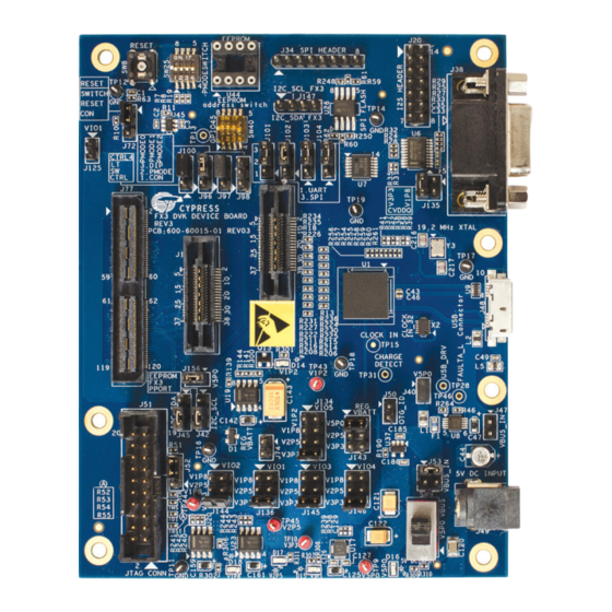
Related Manuals for Cypress EZ-USB FX3 CYUSB3KIT-001


Summary of Contents for Cypress EZ-USB FX3 CYUSB3KIT-001
- Page 1 CYUSB3KIT-001 ® EZ-USB FX3™ Development Kit Guide Doc. #: 001-70237 Rev. *C Cypress Semiconductor 198 Champion Court San Jose, CA 95134-1709 Phone (USA): +1.800.858.1810 Phone (Intnl): +1.408.943.2600 http://www.cypress.com Arrow.com. Downloaded from...
- Page 2 Cypress Source Code and derivative works for the sole purpose of creating custom soft- ware and or firmware in support of licensee product to be used only in conjunction with a Cypress integrated circuit as speci- fied in the applicable agreement.
-
Page 3: Table Of Contents
Example 1: Blinking LED and push button ..............18 2.6.1 FX3 Firmware Download and Debug Methods ..........20 2.6.2 Code Structure ....................33 Importing All of the Cypress Examples ..............34 3. Kit Operation Default Jumper Settings on DVK Board ..............35 Bus-Power Mode .......................36 Self-Power Mode .......................36... - Page 4 Contents 3.11 Example 2: Loopback of Data over Bulk Endpoints...........55 3.12 Modify the Bulkloop Firmware Example ..............57 3.13 Example 3: Measurement of Throughput Using USB 3.0 Bulk Transfers....62 4. Hardware Power Supply......................65 USB Receptacle ......................66 Clocking Mechanism for FX3 ..................67 GPIF II Connector......................69 4.4.1 Interconnecting to the GPIF II Connector............73 4.4.2 FX3 DVK Interconnect Boards ...............76...
-
Page 5: Introduction
Installer: It installs the Eclipse IDE and GCC tool chain, a ■ firmware library with code samples, and a Cypress USB suite including a Windows driver and sample Visual Studio applications. After installation, a Cypress Update Manager insures that all modules are up to date. -
Page 6: Other Suggested Tools
Software protocol analyzers SourceQuest SourceUSB ❐ SysNucleus USBTrace ❐ Additional Learning Resources Visit http://www.cypress.com/fx3 for additional learning resources in the form of datasheets, a technical reference manual, and application notes. Document History PDF Creation Origin of Revision Description of Change... -
Page 7: Abbreviations
Introduction Abbreviations Table 1-2. List of Abbreviations Abbreviation Meaning Alternating Current ADMUX Address Data Multiplexing ASIC Application-Specific Integrated Circuit COM port Communication Port UART Clear To Send Direct Current Digital Signal Processor Development Kit EEPROM Electrically Erasable Programmable Read-only memory Endpoint Electrostatic discharge FPGA Mezzanine Card... -
Page 8: Getting Started
Getting Started This chapter guides you through the installation of the Windows versions of the FX3 DVK and FX3 Software Development Kit (SDK). After installing the Eclipse-based tools, a simple example confirms that the installation is correct and introduces the Eclipse system. FX3 DVK Software Installation To install the kit software, follow these steps: 1. - Page 9 Getting Started 2. Select the required Installation Type and click the Next button to start the Installation Wizard (Figure 2-2). For the first time installation it is recommended to Installation Type as Typical. Figure 2-2. Installation Wizard CYUSB3KIT-001 EZ-USB FX3 Development Kit Guide, Doc. #: 001-70237 Rev. *C Arrow.com.
- Page 10 Getting Started 3. Accept the license agreements for the various software components and click Next and wait till the installation is complete. Figure 2-3. Installation Progress Showing Individual Modules CYUSB3KIT-001 EZ-USB FX3 Development Kit Guide, Doc. #: 001-70237 Rev. *C Arrow.com.
- Page 11 Getting Started 4. When installation completes you have the option to run the Cypress Update Manager (Figure 2-4), to insure you have the latest SDK. Click the Check for Updates button at the bottom of the Cypress Update Manager window. If No Updates appears against EZ-USB FX3 SDK you can click Exit button.
-
Page 12: Fx3 Sdk Installation
Getting Started FX3 SDK Installation Note: If you ran the Cypress Update Manager after installing the DVK and downloaded the latest version of the SDK you can skip the steps listed in this section. To install the latest version of FX3 SDK, follow these steps: 1. -
Page 13: Rolling Back To A Previous Version Of Fx3 Sdk
Figure 2-6. Installation Progress Showing Individual Modules Rolling Back to a Previous Version of FX3 SDK You can roll back to any previous version of FX3 SDK using Cypress Update Manager. Use the steps given in the Knowledge Base article to install any previous version. -
Page 14: Eclipse Ide Quick Tour
Eclipse IDE Quick Tour 2.5.1 Start Eclipse Navigate to Windows > Start > All Programs, and then click on the Cypress folder to expand it (Figure 2-7). Installed Cypress software packages appear, including GPIF II Designer, a utility to create design files for the FX3 General Programmable Interface (GPIF II) using state machine entry. -
Page 15: Import A Project
C:\Program Files\Cypress\EZ-USB FX3 SDK\firmware. For 64-bit systems the first folder in the path is Program Files(x86). Later in this chapter you will import all of the Cypress examples into your Workbench, but first it is helpful to learn how an Eclipse project is imported from anywhere, for example from another computer, an email or a colleague. - Page 16 Getting Started 2. In the Eclipse IDE, select File > Import > General > Existing Projects into Workspace (Figure 2-9). Click Next button. Figure 2-9. Import an Eclipse Project 3. Select the Browse… button next to Select root directory: and browse to your First_FX3_App folder (Figure 2-10).
-
Page 17: Tweak Eclipse Ide Settings
Getting Started 5. To build a FX3 project, select the project in the Project Explorer window and click the Build button (hammer) in the Eclipse IDE. You can choose whether you want to build a Debug version or a Release version of the firmware. The size of the generated image file in the Release version is smaller than that in the debug version. -
Page 18: Example 1: Blinking Led And Push Button
Getting Started Example 1: Blinking LED and push button The first_app.c code blinks an LED attached to a GPIO (General-Purpose IO) pin and reads the state of a GPIO input pin, printing its state on a Windows terminal whenever the state changes. To see the results of this application, prepare the small circuit shown in Figure 2-14. - Page 19 Getting Started Most FX3 GPIO pins can be programmed to attach an internal pull-up or pull-down resistor to prevent floating inputs. This example uses two GPIO pins that are programmed as a group to serve as UART signals. Because the serial debugger does not use the UART CTS and RTS signals, these pins can be used for the LED and push button.
-
Page 20: Fx3 Firmware Download And Debug Methods
2. Move the slide switch (SW9) in the lower right corner of the board to the UP position. This sup- plies board power from USB, eliminating the need for an external power unit. 3. The board enumerates as a Cypress BootLoader, as seen in the Device Manager tree (Figure 2-16). - Page 21 USB device, so the Cypress USB BootLoader item disappears from the USB Control Center device window. Most Cypress examples implement USB devices, in which case you will see the new device name appear in place of the Cypress USB BootLoader device.
- Page 22 Getting Started 2.6.1.2 Run Code with Serial Debug This debug method gives feedback from a running program via the FX3 UART port. Since modern PC’s do not include serial ports, you will need a serial-to-USB converter such as the Keyspan (Tripp Lite) USA-19-HS (Figure 2-19).
- Page 23 Getting Started 3. Choose Setup > Serial Port and adjust the baud rate to 115,200. Then press OK (Figure 2-21). Figure 2-21. Select 115,200 baud rate 4. Load and run the code as in the first example. To recap: If the USB Control Panel is not already running, choose CY Tools>Control Center, press the board RESET button, choose Program>FX3>RAM, navigate to the .img file in your Workspace and load the program.
- Page 24 Getting Started 2.6.1.3 Download and Debug over JTAG This debug method uses FX3 on-chip debug logic which is accessed over a JTAG (Joint Test Action Group) port. JTAG debug may coexist with serial port debug since any code can access the debug print function.
- Page 25 Getting Started Start the Segger J-Link GDB Server (Figure 2-25). Click OK to accept the default settings. Figure 2-25. Segger J-Link Startup Screen The J-Link GDB Server screen appears as in Figure 2-26. This screen runs concurrently with your Eclipse sessions, so you can drag this window off to a side of your desktop.
- Page 26 The following steps configure the Eclipse project to be compatible with the J-Link debugger. Some Cypress projects are already configured, so you only need to confirm the settings. Once a project is configured the settings are in force for all subsequent debug sessions.
- Page 27 Getting Started 3. In the Main tab, click the Search Project… button and select the .elf (executable and linkable) file shown there (Figure 2-29). You can name the debug profile anything you want. Figure 2-29. Search Project for Executable (elf) File CYUSB3KIT-001 EZ-USB FX3 Development Kit Guide, Doc.
- Page 28 GDB Debugger at the path shown in Figure 2-30. (GDB stands for Gnu debugger.) Program Files (or Program Files (x86))\Cypress\EZ-USB FX3 SDK\version\bin\arm-none-eabi-gdb.exe. Figure 2-30. Browse to Path to GDB Debugger CYUSB3KIT-001 EZ-USB FX3 Development Kit Guide, Doc. #: 001-70237 Rev. *C Arrow.com.
- Page 29 Getting Started 5. Select the Commands tab, and copy and paste the text shown in Figure 2-31 into the ‘Initialize’ commands text box. Figure 2-31. Copy/Paste Text into ‘Initialize’ commands box set prompt (arm-gdb) # This connects to a target via netsiliconLibRemote # listening for commands on a TCP port on the local machine.
- Page 30 Getting Started 6. In the ‘Run’ commands box, type “load”. The Commands tab should now look like that shown in Figure 2-32. Figure 2-32. Filled-in Commands Screen 7. Click the Debug button to start a debug session. You are given the option of switching to the Debug Perspective.
- Page 31 Getting Started 8. You should see a burst of activity in the J-Link Server window as the FX3 code loads over JTAG. When the activity stops the FX3 code execution stops inside an internal code module that is not visible to the debugger. To get past this, click the Resume button (Figure 2-34) or press [F8].
- Page 32 Getting Started 9. The first code line in the main function is highlighted. Pressing [F6] single-steps through the code. You can set and clear breakpoints by double-clicking lines of code. Figure 2-35. Set and clear breakpoints 10.Click the Terminate button to stop a debug session. To return to the code development perspective, select the C/C++ perspective as shown in Figure 2-33.
-
Page 33: Code Structure
FX3 code development uses an RTOS (real-time operating system) called ThreadX to manage high performance applications. Refer to the FX3 Programmers Manual.pdf file available in the documentation folder of the FX3 SDK (C:\Program Files (x86)\Cypress\EZ-USB FX3 SDK\1.3\doc) to get a detailed explanation of example FX3 application source code. -
Page 34: Importing All Of The Cypress Examples
3. Select Copy projects into workspace to make your own local copies, and then click Finish. Figure 2-38. Import All Cypress Example Projects The Eclipse Project Explorer window now contains all the Cypress example projects. To work on an individual project, select it in the Project Explorer window. The project name is highlighted so you can tell at a glance which project you are editing, building and debugging. -
Page 35: Kit Operation
Kit Operation The FX3 DVK board provides convenient access to FX3 interfaces such as I C, SPI, UART and I The DVK board also provides a high-speed (Samtec) connector for interface to external devices through the GPIF II (General Programmable Interface, Gen 2). FX3 SDK examples help you evaluate and program each of these interfaces. -
Page 36: Bus-Power Mode
Kit Operation Bus-Power Mode The FX3 DVK board can operate in bus-power mode. Follow these steps: 1. Verify that pins 1–3 or 2–4 of jumper J53 are shorted. 2. Use the toggle switch SW9 to power ON the board. The switch should point to the direction labeled VBUS_IN instead of V5P0, as shown in Figure 3-1. - Page 37 Kit Operation 2. Plug the 5-V power supply adapter supplied with the kit into the J49 power jack. Use the toggle switch SW9 to power the board. The switch should point to the direction labeled V5P0 instead of VBUS_IN as shown in Figure 3-2.
-
Page 38: First Time Usb Enumeration
Kit Operation First Time USB Enumeration When the FX3 board is powered for the first time, connect the USB 3.0 A to Micro-B cable supplied with the kit to the J48 connector, as shown in Figure 3-3. Figure 3-3. USB 3.0 Cable to J48 Connector Note The bootloader in FX3 ROM by default enumerates as USB 2.0 device. -
Page 39: Manual Installation Of Cypress Driver
Kit Operation 3.4.1 Manual Installation of Cypress Driver 1. In Windows, invoke Start > Computer and right-click Properties > Select Device Manager. Locate the FX3 device entry with a yellow symbol in the Other Devices list. Sometimes, the FX3 DVK enumerates as Westbridge, as shown in Figure 3-4. - Page 40 C:\Program Files (x86)\Cypress\EZ-USB FX3 SDK\1.3\driver\win7\x64. Your SDK version number may be higher than 1.3. The Device Manager window should remove the WestBridge entry and identify the FX3 DVK board as the Cypress USB BootLoader (top entry) as shown in Figure 3-6.
-
Page 41: Boot Options
Kit Operation Boot Options FX3 provides several booting options. The boot option is determined by the FX3 PMODE[2:0] input pins. These PMODE[2:0] pins are configured using combination of Jumpers (J98, J97, and J96) and dip switch SW25. For I C and SPI boot options additional jumpers (J42, J45, J101, J102, J103, and J104) and a dip switch (SW40) needs to be configured. - Page 42 Kit Operation Table 3-2 shows the FX3 boot interfaces according to the PMODE[2:0] settings. “USB Fallback” means that USB is used to boot code if the indicated interface is not present. Table 3-2. Boot Options with PMODE Pins PMODE2 Pin PMODE1 Pin PMODE0 Pin Boot Option...
-
Page 43: Usb Boot
PMODE0 2. SW25.1 set to OFF 2. Open the USB Control Center application by clicking Start > All Programs > Cypress > Cypress USBSuite > Control Center. When connected to a USB host, the FX3 device enumer- ates in the USB Control Center as Cypress USB BootLoader, as shown in Figure 3-8. - Page 44 Kit Operation 3. In the USB Control Center, choose Program > FX3 > RAM, as shown in Figure 3-9. Figure 3-9. Choose FX3 RAM from the USB Control Center 4. Browse to the firmware image (.img) file to be programmed into the FX3 RAM. Double-click on the .img file, as shown in Figure 3-10.
-
Page 45: I2C Boot
Kit Operation C Boot The FX3 DVK board provides an I C interface as one of the boot options. Mount an I C EEPROM (for e.g., 24LC1025 or 24LC1026) into the U44 socket and verify this feature by programming the firmware image. - Page 46 C clock (SCL) and data line (SDA) jumpers J42 and J45 pins 1–2 should be shorted on the DVK board. 6. When connected to a USB host, the FX3 device enumerates in USB Control Center as Cypress USB BootLoader. 7. In Control Center, select the FX3 device and then choose Program > FX3 > I2C EEPROM. This...
- Page 47 Kit Operation Figure 3-15. Select Firmware Image to Download Figure 3-16. I C EEPROM Programming Update in Control Center CYUSB3KIT-001 EZ-USB FX3 Development Kit Guide, Doc. #: 001-70237 Rev. *C Arrow.com. Arrow.com. Arrow.com. Arrow.com. Arrow.com. Arrow.com. Arrow.com. Arrow.com. Arrow.com. Arrow.com. Arrow.com.
-
Page 48: Booting From I2C Eeprom
Kit Operation 3.7.2 Booting from I C EEPROM Change the PMODE pins on the DVK board to Z1Z to enable I2C boot. On the DVK board, this is done by configuring the jumpers and switches, as shown in Table 3-6. Press RESET button SW8. The FX3 DVK board re-enumerates with the boot image in the I C EEPROM. - Page 49 Kit Operation Figure 3-18. SW40 and EEPROM Interconnect ❐ The firmware image has a fixed header format to boot from the I C EEPROM. After the 2-byte “CY” signature, the third byte bits[3:1] can be used to specify the EEPROM size format. The parameter "bImageCTL"...
-
Page 50: Spi Boot
3. When the FX3 DVK board is connected to a USB PC host using the USB 3.0 cable, the FX3 device enumerates in Control Center as Cypress USB Bootloader. 4. Verify the SPI mode related jumper settings, as shown in Table 3-8. - Page 51 5. In the USB Control Center, select Program > FX3 > SPI FLASH. The USB Control Center application downloads the Serial Flash programming code, and the FX3 DVK board reconnects to USB as Cypress USB BootProgrammer, as shown in Figure 3-21.
- Page 52 Kit Operation 6. After the FX3 DVK board enumerates as Cypress USB BootProgrammer, the USB Control Center application prompts the user to select the firmware binary to download. Browse to the relevant img file and select the code image, as shown in Figure 3-22.
-
Page 53: Booting From Spi Flash
Kit Operation 7. The application downloads the firmware into the flash memory. The download status appears at the bottom left corner of the USB Control Center application, as shown in Figure 3-23. Figure 3-23. SPI Firmware Download Update in USB Control Center 3.8.2 Booting from SPI Flash After programming the firmware to SPI flash, set the PMODE[2:0] pins to 0Z1 to enable SPI boot. -
Page 54: Admux Boot
Kit Operation ADMUX Boot The FX3 device can boot from the synchronous and asynchronous ADMux interface if the PMODE[2:0] pins are set to Z00 and Z01, respectively. For more details, see application note AN76405 - EZ-USB FX3 Boot Options. 3.10 USB 3.0 Enumeration The FX3 DVK board bootloader operates as a USB 2.0 device. -
Page 55: Example 2: Loopback Of Data Over Bulk Endpoints
Download Firmware Image to FX3 RAM on page 3. In the Windows Device Manager, the board appears as Cypress USB BulkloopExample under Universal Bus Controllers. If the board is not listed, bind the driver manually using the steps... - Page 56 Kit Operation 5. Select Bulk out endpoint (0x1) in the left pane of Control Center. Enter AA in Data to send (Hex), and 1 in Bytes to Transfer, and click the Transfer Data-OUT button. Figure 3-26 illustrates these steps. Figure 3-26. Sequence of steps for transferring data 6.
-
Page 57: Modify The Bulkloop Firmware Example
Kit Operation 3.12 Modify the Bulkloop Firmware Example The firmware examples can be modified and recompiled using the Eclipse IDE. The modified firmware binary can then be downloaded to FX3 RAM and tested using a SuiteUSB application. To demonstrate the modification, the USBBulkLoopAuto firmware example of FX3 SDK is used. The bulk endpoint number and its associated socket are modified here to simply demonstrate how to modify, recompile the firmware example, and test the functionality using a PC application. - Page 58 Kit Operation Figure 3-29. cyfxbulklpauto.c Code Snippet The endpoint number and the associated socket are defined in .h using the macros CY_FX_EP_PRODUCER, CY_FX_EP_CONSUMER, CY_FX_EP_PRODUCER_SOCKET, and CY_FX_EP_CONSUMER_SOCKET. Figure 3-30 shows the code snippet defined in this file. To understand sockets, refer to the “FX3 Terminology” section in the application note AN75705 –...
- Page 59 Kit Operation Using these macros, the endpoint number and associated socket are changed from EP1 to EP2 (Figure 3-31). Now EP2 acts as the Bulk IN and OUT endpoints in the modified firmware. Figure 3-31. Endpoint Number and Associated Socket Modified from EP1 to EP2 CYUSB3KIT-001 EZ-USB FX3 Development Kit Guide, Doc.
- Page 60 Kit Operation Build the modified firmware example. You can also build a project as shown in Figure 3-32. Build the firmware example in both debug and release modes by choosing Build Configuration > Set Active > Debug/Release. Figure 3-32. Selecting Build Configuration in Eclipse IDE Note Release code images are smaller than Debug code images.
- Page 61 USB Boot on page 43 to download the firmware image to FX3 RAM using Control Center. The FX3 DVK board enumerates as Cypress USB BulkloopExample in Control Center. Observe that the modified firmware example shows EP2 as both Bulk IN and OUT in Control...
-
Page 62: Example 3: Measurement Of Throughput Using Usb 3.0 Bulk Transfers
Download Firmware Image to FX3 RAM on page 3. In the Windows Device Manager, the board appears as Cypress USB StreamerExample under Universal Bus Controllers. If the board is not listed, bind the driver manually using the steps... - Page 63 Kit Operation Figure 3-35. FX3 device enumeration 4. Run Streamer.exe from the location C:\Program Files (x86)\Cypress\EZ-USB FX3 SDK\1.3\application\cpp\streamer\x86\Release. As shown in Figure 3-36, choose 256 as Packets per Xfer and 32 as Xfers to Queue from the dropdown list available on the Streamer application.
- Page 64 Kit Operation 5. Click the Start button to see the throughput of USB 3.0 bulk IN transfers. The throughput shown with the default bulk source sink firmware image is about 267 MBps (Figure 3-37). Figure 3-37. Throughput of USB 3.0 Bulk IN transfers ...
-
Page 65: Hardware
Hardware This chapter describes the different hardware interfaces available on the FX3 DVK. It explains the following DVK board components: Power supply ■ USB 3.0 Micro-B receptacle connector ■ ■ Clocking mechanism using on-board crystal GPIFII connector ■ Reset circuit ■... -
Page 66: Usb Receptacle
Hardware Table 4-1. Power Supply Domain Power Domain Jumper Jumper positions Voltage levels 1–8 (labeled V1P2 on board) 1.2 V 2–7 (labeled V1P8 on board) 1.8 V VIO5 J134 3–6 (labeled V2P5 on board) 2.5 V 4–5 (labeled V3P3 on board) 3.3 V 1–6 (labeled V2P5 on board) 2.5 V... -
Page 67: Clocking Mechanism For Fx3
Hardware The DVK board supports USB 3.0 peripheral and Hi-Speed OTG functionality using the J48 connector. Table 4-2 shows the jumper settings required to operate in USB 2.0 OTG device or Host mode. Table 4-2. OTG/Host Mode Jumper Settings Jumper Pin Position Mode: Description OTG Host: To supply VBUS to the connected peripheral as OTG host... - Page 68 Hardware FX3 supports a 19.2-MHz crystal, while the supported external clock frequencies are 19.2, 26, 38.4, and 52 MHz. The FSLC[2:0] pins are configured to select the crystal- or clock-frequency option. The configuration options are shown in Table 4-3. Table 4-3. Crystal/Clock Frequency Selection FSLC[2] FSLC[1] FSLC[0]...
-
Page 69: Gpif Ii Connector
Hardware GPIF II Connector The GPIF II interface enables functionality similar to but more advanced than FX2LP's GPIF. It is a programmable state machine that enables a flexible interface, which functions either as a master or a slave using industry standard or proprietary interfaces. You can implement both parallel and serial interfaces with GPIF II. - Page 70 Hardware Figure 4-6. Samtec Expansion Connector Circuit1 J77A J77A QSH-060 QSH-060 VIO1_HDR VIO1_HDR SEC 1/2 SEC 1/2 PMODE2_CON {2} {2,4} CTL3 DQ6 {2,4} {2,4} CTL0 PMODE0_CON {2} {2,4} CTL7 DQ28 {4,5} {2,4} CTL5 DQ30 {4,5} {2,4} CTL9 DQ7 {2,4} {2,4} CTL10 PCLK {2,4} {2,4}...
- Page 71 Hardware Figure 4-7. Samtec Expansion Connector Circuit 2 J77B J77B QSH-060 QSH-060 {2,4} DQ10 DQ29 {4,5} SEC 2/2 SEC 2/2 {4,5} DQ26 DQ31 {4,5} {2,4} DQ14 DQ8 {2,4} {4,5} DQ23 DQ0 {2,4} {4,5} DQ22 DQ3 {2,4} {2,4} DQ12 DQ25 {4,5} {4,5} DQ18 DQ1 {2,4}...
- Page 72 Hardware Table 4-4. FX3 GPIF II Signal Pinout on Samtec Connector (continued) Connector J77 Pin No. FX3 Signals GPI/O GPIO[8] GPIO[9] GPIO[10] GPIO[11] GPIO[12] GPIO[13] GPIO[14] GPIO[15] GPIO[16] CTL0 GPIO[17] CTL1 GPIO[18] CTL2 GPIO[19] CTL3 GPIO[20] CTL4 GPIO[21] CTL5 GPIO[22] CTL6 GPIO[23] CTL7...
-
Page 73: Interconnecting To The Gpif Ii Connector
Hardware Table 4-4. FX3 GPIF II Signal Pinout on Samtec Connector (continued) Connector J77 Pin No. FX3 Signals GPI/O D29_UART-CTS GPIO[47] D30_UART-TX GPIO[48] D31_UART-RX GPIO[49] I2S-CLK GPIO[50] I2S-SD GPIO[51] I2S-WS GPIO[52] I2S-MCLK GPIO[57] I2C-SCL GPIO[58] I2C-SDA GPIO[59] As shown in Figure 4-7, a jumper J125 can be inserted to enable the VIO1 (1.8 V, 2.5 V, and 3.3 V –... - Page 74 Hardware Figure 4-9. Clearance to Samtec Connector (all dimensions in mils) CYUSB3KIT-001 EZ-USB FX3 Development Kit Guide, Doc. #: 001-70237 Rev. *C Arrow.com. Arrow.com. Arrow.com. Arrow.com. Arrow.com. Arrow.com. Arrow.com. Arrow.com. Arrow.com. Arrow.com. Arrow.com. Arrow.com. Arrow.com. Arrow.com. Arrow.com. Arrow.com. Arrow.com. Arrow.com. Arrow.com.
- Page 75 Hardware Figure 4-10. Distance from Center of Pin 1 to Top Edge of Board (all dimensions in mils) Figure 4-11. Distance from Center of Pin 1 to Left Edge of Board (all dimensions in mils) CYUSB3KIT-001 EZ-USB FX3 Development Kit Guide, Doc. #: 001-70237 Rev. *C Arrow.com.
-
Page 76: Fx3 Dvk Interconnect Boards
For the HSMC interconnect board, visit http://www.cypress.com/?app=forum&id=167&rID=84756 For the Aptina interconnect board, contact Cypress at fx3@cypress.com. Reset Circuit The FX3 device can be reset either from an external processor wired to the Samtec connector or from an on-board push button. This selection can be made on J72; see Figure 4-12. -
Page 77: Serial Interfaces
Hardware Serial Interfaces EZ-USB FX3 supports the following serial interfaces: ■ ■ SPI and UART ■ JTAG ■ 4.6.1 I2C Interface The I2C interface lines on the FX3 device are available on headers for probing and expansion, as well as to connect to an on-board EEPROM device. You can set the EEPROM address bits A2, A1, and A0 using the on-board dip switch SW40. - Page 78 Hardware Figure 4-14. SPI/UART Selection Headers on DVK Note The arrow marked near the jumpers indicates pin1 of the jumper. Figure 4-15 shows the jumper J101–J104 schematic symbols and the signal names (UART/SPI) on each of these jumper pins. CYUSB3KIT-001 EZ-USB FX3 Development Kit Guide, Doc. #: 001-70237 Rev. *C Arrow.com.
- Page 79 Hardware Figure 4-15. UART/SPI Selection Headers J101 J101 UART_RTS {6} SPI-SCK_UART-RTS SPI_CLK HEADER_1x3_100mil HEADER_1x3_100mil J102 J102 UART_CTS {6} SPI-SSN_UART-CTS SPI_SSN HEADER_1x3_100mil HEADER_1x3_100mil J103 J103 UART_TX {6} SPI-MISO_UART-TX SPI_MISO HEADER_1x3_100mil HEADER_1x3_100mil J104 J104 UART_RX {6} SPI-MOSI_UART-RX SPI_MOSI HEADER_1x3_100mil HEADER_1x3_100mil Table 4-5 shows the jumper J101–J104 pin combination to select either the UART or SPI interface.
-
Page 80: Jtag
Hardware Figure 4-16. Flash Circuit of DVK Board SPI Flash VIO4 VIO4 100K 100K R252 R252 SPI_MOSI_flash 100K 100K R246 R246 SPI_MISO_flash 100K 100K R247 R247 SPI_CLK_flash 0.1uF 0.1uF VIO4 4.7K 4.7K R248 R248 SPI_Hold#_flash HOLD 4.7K 4.7K R249 R249 SPI_SSN_flash 4.7K 4.7K... -
Page 81: Appendix - Troubleshooting
If the FX3 DVK board does not power up even after the power adapter has been replaced, the board may be faulty. Contact http://www.cypress.com/go/support technical assistance Bus-Power Mode Problem Possible Cause Possible Solution Incorrect switch setting Set switch SW9 to “VBUS_IN”... -
Page 82: Usb 2.0 Enumeration
USB 2.0 Enumeration Problem Possible Cause Possible Solution If the board is powered first and then Sequence of operations connected to the PC, it may not enumerate. User should hit the reset button in this case. If the DVK board is self-powered, ensure that Incorrect power mode the jumper settings are as shown in “Self-... -
Page 83: Usb Boot
USB Boot Problem Possible Cause Possible Solution Verify that PMODE [2:0] pin settings for USB Incorrect PMODE settings boot are as specified in Table 3-5 Limitation of Etron host controller. (The Control Center application in SDK builds Migrate to FX3 SDK version 1.2.1 or later. prior to version 1.2.1 (In FX3 SDK 1.2.1, the control transfer size for Control Center displays... -
Page 84: I2C Boot
I2C Boot Problem Possible Cause Possible Solution Verify correct EEPROM orientation in socket Incorrect EEPROM mounting Make sure that the EEPROM has enough capacity to hold the .img file. To find the size of EEPROM size the .img file, right click on the .img file and choose “properties”. -
Page 85: Usb3.0 Enumeration
USB3.0 Enumeration Problem Possible Cause Possible Solution Applicable only to NEC host controllers - Excessive spread spectrum reference clock from motherboard chipset. (The NEC host controller does not have its own reference Check the Spread Spectrum setting in the PC clock for USB 3.0. -
Page 86: Appendix - Pcb Layout
Appendix - PCB Layout Assembly Top CYUSB3KIT-001 EZ-USB FX3 Development Kit Guide, Doc. #: 001-70237 Rev. *C Arrow.com. Arrow.com. Arrow.com. Arrow.com. Arrow.com. Arrow.com. Arrow.com. Arrow.com. Arrow.com. Arrow.com. Arrow.com. Arrow.com. Arrow.com. Arrow.com. Arrow.com. Arrow.com. Arrow.com. Arrow.com. Arrow.com. Arrow.com. Arrow.com. Arrow.com. Arrow.com. Arrow.com. -
Page 87: Assembly Bottom
Assembly Bottom CYUSB3KIT-001 EZ-USB FX3 Development Kit Guide, Doc. #: 001-70237 Rev. *C Arrow.com. Arrow.com. Arrow.com. Arrow.com. Arrow.com. Arrow.com. Arrow.com. Arrow.com. Arrow.com. Arrow.com. Arrow.com. Arrow.com. Arrow.com. Arrow.com. Arrow.com. Arrow.com. Arrow.com. Arrow.com. Arrow.com. Arrow.com. Arrow.com. Arrow.com. Arrow.com. Arrow.com. Arrow.com. Arrow.com. Arrow.com. Arrow.com.
Need help?
Do you have a question about the EZ-USB FX3 CYUSB3KIT-001 and is the answer not in the manual?
Questions and answers