Table of Contents
Advertisement
Quick Links
Jacinto7 J721E/DRA829/TDA4VM Evaluation Module
This technical user's guide describes the hardware architecture and configuration options of the
J721E/DRA929/TDA4VM EVM.
...................................................................................................................
1
1.1
1.2
1.3
2
2.1
2.2
2.3
2.4
3
3.1
3.2
3.3
3.4
3.5
3.6
4
4.1
4.2
4.3
4.4
4.5
4.6
4.7
4.8
4.9
4.10
4.11
4.12
4.13
4.14
4.15
4.16
4.17
4.18
4.19
4.20
4.21
4.22
4.23
4.24
SPRUIS4A - December 2019 - Revised May 2020
Submit Documentation Feedback
........................................................................................................
...............................................................................................
................................................................................................
.......................................................................................................
..................................................................................
...........................................................................................
..............................................................................................
................................................................................................
.................................................................................
...................................................................................................
......................................................................................
..................................................................................
.............................................................................................
.....................................................................................................
......................................................................................................
...............................................................................................................
...............................................................................................................
.................................................................................................
..........................................................................................
.......................................................................................
.....................................................................................................
......................................................................................................
......................................................................................................
..............................................................................
..............................................................................
....................................................................................................
............................................................................................
.....................................................................................................
......................................................................................................
.....................................................................................................
.....................................................................................................
....................................................................................
.....................................................................................
Copyright © 2019-2020, Texas Instruments Incorporated
SPRUIS4A - December 2019 - Revised May 2020
Contents
.........................................................................
....................................................
.....................................................................
............................................................................
.............................................................................
.....................................................................
...................................................................
Jacinto7 J721E/DRA829/TDA4VM Evaluation Module (EVM)
User's Guide
(EVM)
5
5
6
7
7
9
10
11
12
13
13
14
18
19
23
24
27
27
29
30
31
32
38
40
43
49
51
53
59
62
65
66
67
67
69
69
71
71
72
73
74
1
Advertisement
Table of Contents

Related Manuals for Texas Instruments Jacinto7 J721E


Summary of Contents for Texas Instruments Jacinto7 J721E
-
Page 1: Table Of Contents
..................... 4.21 ADC Interface ..................... 4.22 RTC Interface ..................4.23 Apple Authentication Header ..................4.24 EVM Expansion Connectors SPRUIS4A – December 2019 – Revised May 2020 Jacinto7 J721E/DRA829/TDA4VM Evaluation Module (EVM) Submit Documentation Feedback Copyright © 2019–2020, Texas Instruments Incorporated... - Page 2 Type C Power Delivery Current Settings ..................USB Hub Reference Clock Circuit ....................USB Hub Settings Circuit ....................USB1 ID Setting for HUB Jacinto7 J721E/DRA829/TDA4VM Evaluation Module (EVM) SPRUIS4A – December 2019 – Revised May 2020 Submit Documentation Feedback Copyright © 2019–2020, Texas Instruments Incorporated...
- Page 3 Resistors for Selecting PCIe Card Host or Device Operation ..............Reference Clock Selection for PCIe Host Operation ............. Reference Clock Selection for PCIe Endpoint Operation SPRUIS4A – December 2019 – Revised May 2020 Jacinto7 J721E/DRA829/TDA4VM Evaluation Module (EVM) Submit Documentation Feedback Copyright © 2019–2020, Texas Instruments Incorporated...
- Page 4 ................... CSI Expansion Connector J48 Pinout Trademarks KeyStone is a trademark of Texas Instruments. Arm is a registered trademark of Arm Limited (or its subsidiaries) in the US and/or elsewhere. All other trademarks are the property of their respective owners.
-
Page 5: Introduction
Introduction The Jacinto7 J721E (DRA829/TDA4xM) EVM is a standalone test, development, and evaluation module system that enables developers to write software and develop hardware around Jacinto7 J721E (DRA829/TDA4xM) processor subsystem. The J721E processor is a KeyStone™ III-based Multicore Arm ®... -
Page 6: Thermal Compliance
Although the processor/heatsink is not a burn hazard, caution should be used when handling the EVM due to increased heat in the area of the heatsink. Figure 1. Thermal Caution Jacinto7 J721E/DRA829/TDA4VM Evaluation Module (EVM) SPRUIS4A – December 2019 – Revised May 2020 Submit Documentation Feedback... -
Page 7: Reach Compliance
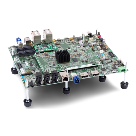
FPD Link Connector D4S20G-400A5-C Lead 7439-92-1 Littelfuse Power fuse 0154010.DR Lead 7439-92-1 J721E EVM Overview Figure 2. J721E EVM Board SPRUIS4A – December 2019 – Revised May 2020 Jacinto7 J721E/DRA829/TDA4VM Evaluation Module (EVM) Submit Documentation Feedback Copyright © 2019–2020, Texas Instruments Incorporated... -
Page 8: System Architecture Interface
The J721E EVM System on Module (SoM) board, a Jacinto7 Common Processor board, and Quad-Port Ethernet Board. Detailed descriptions of these cards are explained in the following sections. Jacinto7 J721E/DRA829/TDA4VM Evaluation Module (EVM) SPRUIS4A – December 2019 – Revised May 2020 Submit Documentation Feedback Copyright ©... -
Page 9: J721E Evm Board Identification
J721E EVM Overview www.ti.com J721E EVM Board Identification Figure 4. J721E EVM Board Identification (SOM, CPB, QP Ethernet) SPRUIS4A – December 2019 – Revised May 2020 Jacinto7 J721E/DRA829/TDA4VM Evaluation Module (EVM) Submit Documentation Feedback Copyright © 2019–2020, Texas Instruments Incorporated... -
Page 10: J721E Som Component Identification
& Power OSPI J5 (DSI0, & DP0) Hyper Flash+ FLASH Hyper RAM Figure 5. J721E SOM Component Identification Jacinto7 J721E/DRA829/TDA4VM Evaluation Module (EVM) SPRUIS4A – December 2019 – Revised May 2020 Submit Documentation Feedback Copyright © 2019–2020, Texas Instruments Incorporated... -
Page 11: Jacinto7 Common Processor Components Identification
Socket Battery Holder Test Automation RGMII DSI FPC Link Connector Serializer Figure 6. Jacinto7 Common Processor Component Identification SPRUIS4A – December 2019 – Revised May 2020 Jacinto7 J721E/DRA829/TDA4VM Evaluation Module (EVM) Submit Documentation Feedback Copyright © 2019–2020, Texas Instruments Incorporated... -
Page 12: Quad Ethernet Components Identification
Bottom ± P2 Bottom ± P0 Clock Quad-SGMII ENET EXP Mating Conn Figure 7. Quad Ethernet Component Identification Jacinto7 J721E/DRA829/TDA4VM Evaluation Module (EVM) SPRUIS4A – December 2019 – Revised May 2020 Submit Documentation Feedback Copyright © 2019–2020, Texas Instruments Incorporated... -
Page 13: Evm User Setup/Configuration
EVM’s 2.5 x 5.5-mm DC barrel jack connector (J7) supports 10-A current rating. Polarity outside barrel is Negative/GND, inside post is Positive/PWR. Figure 8. Connector Used for Power Input SPRUIS4A – December 2019 – Revised May 2020 Jacinto7 J721E/DRA829/TDA4VM Evaluation Module (EVM) Submit Documentation Feedback Copyright © 2019–2020, Texas Instruments Incorporated... -
Page 14: Power On Switch And Power Leds
The power to the EVM is controlled by the power ON/OFF switch (SW2) on the CPB. To turn the board ON, slide the switch in the direction as shown in Figure Figure 9. Power ON/OFF Switch Jacinto7 J721E/DRA829/TDA4VM Evaluation Module (EVM) SPRUIS4A – December 2019 – Revised May 2020 Submit Documentation Feedback Copyright © 2019–2020, Texas Instruments Incorporated... -
Page 15: Power On/Fault Leds
Input voltage is >28 V or <6 V Input voltage is within the limit Figure 10. Power ON/Fault LEDs SPRUIS4A – December 2019 – Revised May 2020 Jacinto7 J721E/DRA829/TDA4VM Evaluation Module (EVM) Submit Documentation Feedback Copyright © 2019–2020, Texas Instruments Incorporated... -
Page 16: Power Status Leds
Regulated Power On/Off VSYS_3V3 SoC Main Domain On/Off VSYS_IO_3V3 SoC MCU Domain On/Off VSYS_MCUIO_3V3 Figure 11. Power Status LEDs Jacinto7 J721E/DRA829/TDA4VM Evaluation Module (EVM) SPRUIS4A – December 2019 – Revised May 2020 Submit Documentation Feedback Copyright © 2019–2020, Texas Instruments Incorporated... -
Page 17: Power Test Points
VDD_SD_DV TP44 3.3V VSYS_MCUIO_3V3 TP113 3.3V VSYS_IO_3V3 TP131 3.3V VSYS_MCUIO_1V8 TP134 1.8V VSYS_IO_1V8 TP132 1.8V VDA_MCU_1V8 TP105 1.8V SPRUIS4A – December 2019 – Revised May 2020 Jacinto7 J721E/DRA829/TDA4VM Evaluation Module (EVM) Submit Documentation Feedback Copyright © 2019–2020, Texas Instruments Incorporated... -
Page 18: Evm Reset/Interrupt Push Buttons
MCAN0_WAKE CAN Wakeup Input RESET PUSH BOTTOMS SW10 EXTINTn SW11 SYS_IRQz SW12 CAN_WK Figure 12. EVM Push Buttons Jacinto7 J721E/DRA829/TDA4VM Evaluation Module (EVM) SPRUIS4A – December 2019 – Revised May 2020 Submit Documentation Feedback Copyright © 2019–2020, Texas Instruments Incorporated... -
Page 19: Evm Dip Switches
Expansion Boards. For those settings, the device-specific Expansion Board User's Guide will define the switch function. Figure 13. EVM Configuration DIP Switch SPRUIS4A – December 2019 – Revised May 2020 Jacinto7 J721E/DRA829/TDA4VM Evaluation Module (EVM) Submit Documentation Feedback Copyright © 2019–2020, Texas Instruments Incorporated... -
Page 20: Evm Configuration Switch Function
USER_INPUT1 User Define, maps to I/O Expander Input ‘0’ (OFF) = User Defined ‘1’ (ON) = User Defined Jacinto7 J721E/DRA829/TDA4VM Evaluation Module (EVM) SPRUIS4A – December 2019 – Revised May 2020 Submit Documentation Feedback Copyright © 2019–2020, Texas Instruments Incorporated... -
Page 21: Evm Configuration Switch Function
Manual method of enabling PMIC ‘0’ (OFF) = PMIC enabled by EVM system ‘1’ (ON) = PMIC enabled manually (test mode only) SPRUIS4A – December 2019 – Revised May 2020 Jacinto7 J721E/DRA829/TDA4VM Evaluation Module (EVM) Submit Documentation Feedback Copyright © 2019–2020, Texas Instruments Incorporated... -
Page 22: Boot Switches Provided On The Processor Card
(SW8.6) (SW8.7) (SW9.8) Primary Boot Backup Boot Mode Primary Boot Mode Config Backup Boot Mode B Mode Config Jacinto7 J721E/DRA829/TDA4VM Evaluation Module (EVM) SPRUIS4A – December 2019 – Revised May 2020 Submit Documentation Feedback Copyright © 2019–2020, Texas Instruments Incorporated... -
Page 23: Evm Uart/Com Port Mapping
– FT2232H (MCU and WKUP) • CPB Serial number: 14197900028 – Programmed Serial number on FT4232H EEPROM: 141979000280B SPRUIS4A – December 2019 – Revised May 2020 Jacinto7 J721E/DRA829/TDA4VM Evaluation Module (EVM) Submit Documentation Feedback Copyright © 2019–2020, Texas Instruments Incorporated... -
Page 24: Jtag Emulation
Function XDS110 Powered via USB HIGH A<->B2 port [On Board EMU] External Emulator attached A<->B1 port [EXTERNAL EMU] Jacinto7 J721E/DRA829/TDA4VM Evaluation Module (EVM) SPRUIS4A – December 2019 – Revised May 2020 Submit Documentation Feedback Copyright © 2019–2020, Texas Instruments Incorporated... -
Page 25: Ti 60 Pin Connector (J16) Pinout
DGND TRC_CTL TRC_DATA14 TRC_DATA19 TRC_DATA0 TRC_DATA15 TRC_DATA20 TRC_DATA1 TRC_DATA16 TRC_DATA21 TRC_DATA2 TRC_DATA17 TRC_DATA3 TRC_DATA18 TRC_DATA4 DGND JTAG_MUX_SEL TRC_DATA5 SPRUIS4A – December 2019 – Revised May 2020 Jacinto7 J721E/DRA829/TDA4VM Evaluation Module (EVM) Submit Documentation Feedback Copyright © 2019–2020, Texas Instruments Incorporated... -
Page 26: Cti20 Pin Connector (J1-Refer Proc081E2 Sch) Pinout
Pin No. Signal MIPI_14_TMS 14PJTAG_DET MIPI_14_TRST MIPI_14_RTCK MIPI_14_TDI DGND MIPI_14_TDIS MIPI_14_TCK MIPI_14_VTREF DGND NC (key) MIPI_14_EMU0 MIPI_14_TDO MIPI_14_EMU1 Jacinto7 J721E/DRA829/TDA4VM Evaluation Module (EVM) SPRUIS4A – December 2019 – Revised May 2020 Submit Documentation Feedback Copyright © 2019–2020, Texas Instruments Incorporated... -
Page 27: J721E Evm Hardware Architecture
Figure 16 shows the functional block diagram of the J721E EVM. Figure 16. J721E EVM Functional Block Diagram SPRUIS4A – December 2019 – Revised May 2020 Jacinto7 J721E/DRA829/TDA4VM Evaluation Module (EVM) Submit Documentation Feedback Copyright © 2019–2020, Texas Instruments Incorporated... -
Page 28: Quad Port Ethernet Expansion Functional Block Diagram
3.3 V REGULATOR TPS74801 (x2) POWER(12 V, 5 V, 3V3) Figure 17. Quad Port Ethernet Expansion Functional Block diagram Jacinto7 J721E/DRA829/TDA4VM Evaluation Module (EVM) SPRUIS4A – December 2019 – Revised May 2020 Submit Documentation Feedback Copyright © 2019–2020, Texas Instruments Incorporated... -
Page 29: J721E Evm Interface Mapping
MCU_MCAN0 TCAN1043-Q1 (W/ Wake function) MCU_MCAN1 TCAN1042HGVD MCAN0 TCAN1043-Q1 (W/ Wake function) MCAN2 TCAN1042HGVD ADC Header MCU_ADC0 TSW-110-07-S-D SPRUIS4A – December 2019 – Revised May 2020 Jacinto7 J721E/DRA829/TDA4VM Evaluation Module (EVM) Submit Documentation Feedback Copyright © 2019–2020, Texas Instruments Incorporated... -
Page 30: I2C Address Mapping
0x44 EVM/CPB SoC_I2C3 FPD Link-III De-serializer (McASP) DS90UB926Q-Q1 0x2C EVM/CPB SoC_I2C6 8 bit I2C GPIO Expander-5 TCA6408ARGTR 0x20 Jacinto7 J721E/DRA829/TDA4VM Evaluation Module (EVM) SPRUIS4A – December 2019 – Revised May 2020 Submit Documentation Feedback Copyright © 2019–2020, Texas Instruments Incorporated... -
Page 31: Gpio Mapping
'1' - no interrupt) I3C0_SCL GPIO1_5 H_I3C0_SCL CP Board Audio De-serializer UB926_GPIO2 I3C0_SDA GPIO1_6 H_I3C0_SDA CP Board Audio De-serializer UB926_GPIO3 SPRUIS4A – December 2019 – Revised May 2020 Jacinto7 J721E/DRA829/TDA4VM Evaluation Module (EVM) Submit Documentation Feedback Copyright © 2019–2020, Texas Instruments Incorporated... -
Page 32: Power Supply
Dual load switch TPS22976-Q1 provides the switching option for the LPDDR4 I/O power supply (1.1 V / 0.6 V). Figure 18. J721E SOM Power Distribution Block Diagram Jacinto7 J721E/DRA829/TDA4VM Evaluation Module (EVM) SPRUIS4A – December 2019 – Revised May 2020 Submit Documentation Feedback... -
Page 33: Power On Sequencing
UB926_PWR_SW_CNTRL* LM5141_PG LM5140_PG2 PORz PMIC_PORz LOAD SW PCIe0_PORz TPS1H100A VCC_12V_DSI0 PWR_SW_CNTL_DSI0* PCIe1_PORz TA_PORZ# Figure 19. Power ON Sequencing SPRUIS4A – December 2019 – Revised May 2020 Jacinto7 J721E/DRA829/TDA4VM Evaluation Module (EVM) Submit Documentation Feedback Copyright © 2019–2020, Texas Instruments Incorporated... -
Page 34: Voltage Supervisor Circuit
The power rails are monitored to control the Power ON Reset (MCU_PORz) for SoC. Two supervisor devices are provided to monitor Main power input and VSYS_3V3. Figure 20. Voltage Supervisor Circuit Jacinto7 J721E/DRA829/TDA4VM Evaluation Module (EVM) SPRUIS4A – December 2019 – Revised May 2020 Submit Documentation Feedback... -
Page 35: Lpddr4 Io Voltage Selection Circuit
SW1 Bit 1 SDRAM_TYPE Selected DDR I/O Voltage LPDDR4X 0.6V HIGH LPDDR4 1.1V Figure 21. LPDDR4 IO Voltage Selection Circuit SPRUIS4A – December 2019 – Revised May 2020 Jacinto7 J721E/DRA829/TDA4VM Evaluation Module (EVM) Submit Documentation Feedback Copyright © 2019–2020, Texas Instruments Incorporated... -
Page 36: J721E Soc S2R Logic Flow
0x65 ENABLE_INT The EVM can be woke from the low power state by the MCU issuing commands to the PMIC through I2C. Jacinto7 J721E/DRA829/TDA4VM Evaluation Module (EVM) SPRUIS4A – December 2019 – Revised May 2020 Submit Documentation Feedback Copyright © 2019–2020, Texas Instruments Incorporated... -
Page 37: Ina Devices I2C Slave Address
SOC_I2C2/PM2 0x4C 0.01E VSYS_3V3 VSYS_3V3_SOM SOC_I2C2/PM2 0x4D 0.01E VDD_EXTLDO1_0V8 VDDA_DLL_0V8 SOC_I2C2/PM2 0x4E 0.01E EXP_3V3 EXP_3V3 SOC_I2C2/PM2 0x4F 0.01E SPRUIS4A – December 2019 – Revised May 2020 Jacinto7 J721E/DRA829/TDA4VM Evaluation Module (EVM) Submit Documentation Feedback Copyright © 2019–2020, Texas Instruments Incorporated... -
Page 38: Reset
Test automation header on the Common processor board also can access these INA devices externally. Reset Figure 22 shows the J721E EVM reset architecture. Jacinto7 J721E/DRA829/TDA4VM Evaluation Module (EVM) SPRUIS4A – December 2019 – Revised May 2020 Submit Documentation Feedback Copyright © 2019–2020, Texas Instruments Incorporated... -
Page 39: Evm Reset Architecture
J721E EVM Hardware Architecture www.ti.com Figure 22. EVM Reset Architecture SPRUIS4A – December 2019 – Revised May 2020 Jacinto7 J721E/DRA829/TDA4VM Evaluation Module (EVM) Submit Documentation Feedback Copyright © 2019–2020, Texas Instruments Incorporated... -
Page 40: Clock
Figure 23. EVM Clock Architecture EVM supports multiple Crystals and Clock generator to provide the reference clock input to the SoC and EVM peripherals. Jacinto7 J721E/DRA829/TDA4VM Evaluation Module (EVM) SPRUIS4A – December 2019 – Revised May 2020 Submit Documentation Feedback... -
Page 41: J721E Soc Primary Clock
PMIC. The OSC1 can be sourced from either the on-board crystal or from clock generator (CDCEL937) on the Common Processor board. SPRUIS4A – December 2019 – Revised May 2020 Jacinto7 J721E/DRA829/TDA4VM Evaluation Module (EVM) Submit Documentation Feedback Copyright © 2019–2020, Texas Instruments Incorporated... -
Page 42: Processor's Secondary/Serdes Ref Clock
<not currently used> 24 MHz NOTE: The probe points mentioned above are with reference to Common processor board. Jacinto7 J721E/DRA829/TDA4VM Evaluation Module (EVM) SPRUIS4A – December 2019 – Revised May 2020 Submit Documentation Feedback Copyright © 2019–2020, Texas Instruments Incorporated... -
Page 43: Memory Interfaces
CS0_A CS1_A DDR0_CSN1_0 DDR0_CKE0 CKE0_A CKE1_A DDR0_CK_T CK_t_A DDR0_CK_C CK_c_A DDR0_RESETn RESET_n DDR0_CAL Figure 25. J721E SoM LPDDR4 SPRUIS4A – December 2019 – Revised May 2020 Jacinto7 J721E/DRA829/TDA4VM Evaluation Module (EVM) Submit Documentation Feedback Copyright © 2019–2020, Texas Instruments Incorporated... -
Page 44: J721E Som Ospi And Hyper Flash
CP board. For more information, see Section 3.4.1. OSPI Hyper Flash Figure 26. J721E SoM OSPI and Hyper Flash Jacinto7 J721E/DRA829/TDA4VM Evaluation Module (EVM) SPRUIS4A – December 2019 – Revised May 2020 Submit Documentation Feedback Copyright © 2019–2020, Texas Instruments Incorporated... -
Page 45: Ufs Memory Block Diagram
UFS0 port of SoC. The UFS memory is Gear3/2Lane capable and supports UFS Version 2.1. Figure 27. UFS Memory Block Diagram SPRUIS4A – December 2019 – Revised May 2020 Jacinto7 J721E/DRA829/TDA4VM Evaluation Module (EVM) Submit Documentation Feedback Copyright © 2019–2020, Texas Instruments Incorporated... -
Page 46: Emmc Memory Block Diagram
200 MHz. External pull up resistors 49.9K are provided on DATA [7:0], CMD and Reset signals, pull down resistor is provided on the data strobe signal to prevent bus floating. Figure 28. eMMC Memory Block Diagram Jacinto7 J721E/DRA829/TDA4VM Evaluation Module (EVM) SPRUIS4A – December 2019 – Revised May 2020 Submit Documentation Feedback... -
Page 47: Micro-Sd Card Block Diagram
SoC. An external pull up resistor (47K) is provided on data [3:0] and CMD signals to avoid floating. SPRUIS4A – December 2019 – Revised May 2020 Jacinto7 J721E/DRA829/TDA4VM Evaluation Module (EVM) Submit Documentation Feedback Copyright © 2019–2020, Texas Instruments Incorporated... -
Page 48: Board Id Memory Header Information
4.8.6 Boot EEPROM Interface A 1-Mbit EEPROM is interfaced to MCU_I2C0 for booting, I2C address set to 0x50, 0x51. Jacinto7 J721E/DRA829/TDA4VM Evaluation Module (EVM) SPRUIS4A – December 2019 – Revised May 2020 Submit Documentation Feedback Copyright © 2019–2020, Texas Instruments Incorporated... -
Page 49: Mcu Ethernet Interface
V and 3.3 V I/O level. The EVM is configured to 3.3 V I/O supply for MCU RGMII PHY I/O signals by default. SPRUIS4A – December 2019 – Revised May 2020 Jacinto7 J721E/DRA829/TDA4VM Evaluation Module (EVM) Submit Documentation Feedback Copyright © 2019–2020, Texas Instruments Incorporated... -
Page 50: Mcu Ethernet Phy Settings
RMGII Clock Skew TX = 0ns RMGII Clock Skew TX = 2ns Figure 31. MCU Ethernet PHY Settings Jacinto7 J721E/DRA829/TDA4VM Evaluation Module (EVM) SPRUIS4A – December 2019 – Revised May 2020 Submit Documentation Feedback Copyright © 2019–2020, Texas Instruments Incorporated... -
Page 51: 4.10 Qsgmii Ethernet Interface
(CDCI2) on the common processor boards will need to be under reset. SPRUIS4A – December 2019 – Revised May 2020 Jacinto7 J721E/DRA829/TDA4VM Evaluation Module (EVM) Submit Documentation Feedback Copyright © 2019–2020, Texas Instruments Incorporated... -
Page 52: Quad-Sgmii Board I2C
The address and clock configurations are shown below: • PHY0: 10000 0X10 • PHY1: 10001 0X11 • PHY2: 10010 0X12 • PHY3: 10011 0X13 Jacinto7 J721E/DRA829/TDA4VM Evaluation Module (EVM) SPRUIS4A – December 2019 – Revised May 2020 Submit Documentation Feedback Copyright © 2019–2020, Texas Instruments Incorporated... -
Page 53: 4.11 Pcie Interface
I2C0 from SoC is used for control purpose and is connected to SMBUS on the connector. I2C0 port is connected to both x1 lane and x2 lane PCIe connectors using a Mux TCA9543APWR. SPRUIS4A – December 2019 – Revised May 2020 Jacinto7 J721E/DRA829/TDA4VM Evaluation Module (EVM) Submit Documentation Feedback Copyright © 2019–2020, Texas Instruments Incorporated... -
Page 54: Pcie Interface For Serdes0
I2C MUX TCA9543A SOC_I2C0_SCL 3.3 V I2CADD: 0x70 PCIe x2 Lane Socket Figure 35. PCIe SMBUS Block Diagram Jacinto7 J721E/DRA829/TDA4VM Evaluation Module (EVM) SPRUIS4A – December 2019 – Revised May 2020 Submit Documentation Feedback Copyright © 2019–2020, Texas Instruments Incorporated... -
Page 55: Reference Clock Selection For Pcie Host Operation
R198 R199, C93 Reference clock for SOC from PCIe R195, C92 R194, R109 connector R199, C93 R198, R110 SPRUIS4A – December 2019 – Revised May 2020 Jacinto7 J721E/DRA829/TDA4VM Evaluation Module (EVM) Submit Documentation Feedback Copyright © 2019–2020, Texas Instruments Incorporated... -
Page 56: Usb2.0 Header Connection
Also, USB2.0 data signals from USB HUB downstream port is interfaced to 4 pin header (J2) and the 5 V supply is provided through the load switch. Figure 37. USB2.0 Header Connection Jacinto7 J721E/DRA829/TDA4VM Evaluation Module (EVM) SPRUIS4A – December 2019 – Revised May 2020 Submit Documentation Feedback... -
Page 57: Pcie Interface For Serdes1
Whereas, in case of PCIe end point operation, the CP board receives reset signal from the PCIe card. Figure 39. 2L-PCIe Root Complex/Endpoint Selection Circuit SPRUIS4A – December 2019 – Revised May 2020 Jacinto7 J721E/DRA829/TDA4VM Evaluation Module (EVM) Submit Documentation Feedback Copyright © 2019–2020, Texas Instruments Incorporated... -
Page 58: Reference Clock Selection For Pcie Host Operation
Table 33. Resistors for Selecting PCIe Card Host or Device Operation Mode Mount Demount Host mode R631 R630 R638 Device mode R630 R631 R638 Jacinto7 J721E/DRA829/TDA4VM Evaluation Module (EVM) SPRUIS4A – December 2019 – Revised May 2020 Submit Documentation Feedback Copyright © 2019–2020, Texas Instruments Incorporated... -
Page 59: 4.12 Usb Interface
(Not supported in J721E SoC) One USB 3.0 Micro AB connector. It is reserved for future J7 family devices. SPRUIS4A – December 2019 – Revised May 2020 Jacinto7 J721E/DRA829/TDA4VM Evaluation Module (EVM) Submit Documentation Feedback Copyright © 2019–2020, Texas Instruments Incorporated... -
Page 60: Usb3.1 Type C Interface
The control signals for Powerdown and VBUS enable are given from I2C GPIO Expander2 (I2C add: 0x22 - P03) and the SoC DRVVBUS, respectively. Jacinto7 J721E/DRA829/TDA4VM Evaluation Module (EVM) SPRUIS4A – December 2019 – Revised May 2020 Submit Documentation Feedback... -
Page 61: Usb Hub Reference Clock Circuit
And the USB ID pin is pulled low to operate the SoC in Host mode. To SoM USB1_ID Pulled low. J721E in Host Mode. Figure 45. USB1 ID Setting for HUB SPRUIS4A – December 2019 – Revised May 2020 Jacinto7 J721E/DRA829/TDA4VM Evaluation Module (EVM) Submit Documentation Feedback Copyright © 2019–2020, Texas Instruments Incorporated... -
Page 62: 4.13 Can Interface
Common processor board bottom left corner. However, the MCU_CAN0 wake feature is disabled by default (resistor population). Only CAN wake-up supported is from MAIN domain. Jacinto7 J721E/DRA829/TDA4VM Evaluation Module (EVM) SPRUIS4A – December 2019 – Revised May 2020 Submit Documentation Feedback... -
Page 63: Can Wake Push Button
Hardware WAKEn input for the CAN interface is provided using a push-button SW12. Figure 47. CAN Wake Push Button SPRUIS4A – December 2019 – Revised May 2020 Jacinto7 J721E/DRA829/TDA4VM Evaluation Module (EVM) Submit Documentation Feedback Copyright © 2019–2020, Texas Instruments Incorporated... -
Page 64: Can Header Connections To Db9/Test Instrument
To interface these CAN signals to Test system, the below given custom converter to be prepared. Figure 48. CAN Header Connections to DB9/Test Instrument Jacinto7 J721E/DRA829/TDA4VM Evaluation Module (EVM) SPRUIS4A – December 2019 – Revised May 2020 Submit Documentation Feedback... -
Page 65: Fpd Interface (Audio Deserializer)
R4 = 40.2K, 1% (or any) R4 = 40.2K, 1% (or any) Figure 50. FPD-Link UB926 Mode Selection Circuit SPRUIS4A – December 2019 – Revised May 2020 Jacinto7 J721E/DRA829/TDA4VM Evaluation Module (EVM) Submit Documentation Feedback Copyright © 2019–2020, Texas Instruments Incorporated... -
Page 66: Fpd Panel Interface (Dsi Video Serializer)
HSD connector J45. Table 35. DSI to FPD Serializer HSD Connector Pinout Pin No Signal DOUT0_P POWER (12V) DOUT0_N Jacinto7 J721E/DRA829/TDA4VM Evaluation Module (EVM) SPRUIS4A – December 2019 – Revised May 2020 Submit Documentation Feedback Copyright © 2019–2020, Texas Instruments Incorporated... -
Page 67: 4.16 Display Serial Interface (Dsi) Fpc
2x digital Outputs from the CODEC is converted to single ended and terminated to stereo Audio jack J40 bottom port using “differential to single ended” converter Line out circuit. SPRUIS4A – December 2019 – Revised May 2020 Jacinto7 J721E/DRA829/TDA4VM Evaluation Module (EVM) Submit Documentation Feedback Copyright © 2019–2020, Texas Instruments Incorporated... -
Page 68: Audio Port Interface Assignment
Line-IN R VIN6 MIC R VIN4 Line-OUT R VOUT8 HPOUT R VOUT4 Figure 52. Audio Port Interface Assignment Jacinto7 J721E/DRA829/TDA4VM Evaluation Module (EVM) SPRUIS4A – December 2019 – Revised May 2020 Submit Documentation Feedback Copyright © 2019–2020, Texas Instruments Incorporated... -
Page 69: 4.18 Display Port Interface
The 12 V and 3.3 V are drawn from the CP board to the connector; the I2C control is provided to the MLB Header from I2C0 port of J721E SoC. SPRUIS4A – December 2019 – Revised May 2020 Jacinto7 J721E/DRA829/TDA4VM Evaluation Module (EVM) Submit Documentation Feedback Copyright © 2019–2020, Texas Instruments Incorporated... -
Page 70: Mlb Interface Connector
H_MLB0_MLBSIG MLB0_MLBDAT_N H_MLB0_MLBDAT MLB0_MLBDAT_P H_MLB0_REFCLK MLB0_MLBCLK_N MLB0_MLBCLK_P DGND DGND MLB0_GPIO0 MLB_RSTz I2C0_SCL MLB_INT# I2C0_SDA VSYS_IO_3V3 VSYS_IO_3V3 VSYS_IO_3V3 VCC_12V0 Jacinto7 J721E/DRA829/TDA4VM Evaluation Module (EVM) SPRUIS4A – December 2019 – Revised May 2020 Submit Documentation Feedback Copyright © 2019–2020, Texas Instruments Incorporated... -
Page 71: 4.20 I3C Interface
NOTE: MCU ADC1 port of J721E SoC is supported on EVM application board (GESI). Figure 55. ADC Interface Connector SPRUIS4A – December 2019 – Revised May 2020 Jacinto7 J721E/DRA829/TDA4VM Evaluation Module (EVM) Submit Documentation Feedback Copyright © 2019–2020, Texas Instruments Incorporated... -
Page 72: 4.22 Rtc Interface
7-bit I2C addresses are 0x57 and 0x6F. VSYS_IO_3V3 Battery VBAT Holder I2C0_SCL (BC501SM) I2C0_SDA MCP79410 J721E SOM RTC_REF_CLK Figure 56. RTC Block Diagram Jacinto7 J721E/DRA829/TDA4VM Evaluation Module (EVM) SPRUIS4A – December 2019 – Revised May 2020 Submit Documentation Feedback Copyright © 2019–2020, Texas Instruments Incorporated... -
Page 73: 4.23 Apple Authentication Header
I2C slave interface, data connection APPLE_AUTH_RSTz Reset, Active low VSYS_IO_3V3 Power 3.3 V DGND Ground 4,6,7, Not Connected 9,10 SPRUIS4A – December 2019 – Revised May 2020 Jacinto7 J721E/DRA829/TDA4VM Evaluation Module (EVM) Submit Documentation Feedback Copyright © 2019–2020, Texas Instruments Incorporated... -
Page 74: 4.24 Evm Expansion Connectors
Either Infotainment or GESI Expansion board can be plugged into EVM expansion connectors (J46 and J51) at once. Figure 58. Expansion Board Interface Connectors Jacinto7 J721E/DRA829/TDA4VM Evaluation Module (EVM) SPRUIS4A – December 2019 – Revised May 2020 Submit Documentation Feedback... -
Page 75: Evm Expansion Connector J46 Pinout
MCASP0_AXR4/PRG0_RGMII1_RXC MCASP0_AXR11/PRG0_RGMII1_TX_CTL PRG0_RGMII1_RD2 MCASP0_AXR10/PRG0_RGMII1_TD3 MCASP0_AXR1/PRG0_RGMII1_RD1 MCASP0_AXR9/PRG0_RGMII1_TD2 PRG0_RGMII1_RD3 MCASP0_AXR12/PRG0_RGMII1_TXC DGND DGND MCASP1_AXR8/PRG0_RGMII2_TD1 MCASP6_ACLKX/PRG1_RGMII1_RD0 MCASP1_AXR7/PRG0_RGMII2_TD0 MCASP6_AFSR/PRG1_RGMII1_RXC GPIO0_79/PRG0_RGMII2_TXC MCASP6_AFSX/PRG1_RGMII1_RD1 PRG0_RGMII2_TD2 PRG1_RGMII1_RD3 SPRUIS4A – December 2019 – Revised May 2020 Jacinto7 J721E/DRA829/TDA4VM Evaluation Module (EVM) Submit Documentation Feedback Copyright © 2019–2020, Texas Instruments Incorporated... - Page 76 PRG0_MDIO0_MDIO/I2C5_SCL SPI3_D0 MCASP0_AXR13/PRG0_PWM0_B2 SPI3_D1 SPI3_CLK RGMII_REFCLK DGND DGND I2C0_SCL MCASP1_ACLKX I2C0_SDA SOC_I2C2_SCL I2C1_SCL SOC_I2C2_SDA I2C1_SDA EXP_RSTz DGND DGND Jacinto7 J721E/DRA829/TDA4VM Evaluation Module (EVM) SPRUIS4A – December 2019 – Revised May 2020 Submit Documentation Feedback Copyright © 2019–2020, Texas Instruments Incorporated...
-
Page 77: Evm Expansion Connector J51 Pinout
GPMC0_A10 GPMC0_A19 GPMC0_A12 GPMC0_A13 DGND DGND DGND VSYS_5V0 DGND VSYS_5V0 DGND VSYS_5V0 MCU_ADC1_AIN0 MCU_ADC1_AIN1 MCU_ADC1_AIN2 MCU_ADC1_AIN3 MCU_ADC1_AIN4 MCU_ADC1_AIN5 SPRUIS4A – December 2019 – Revised May 2020 Jacinto7 J721E/DRA829/TDA4VM Evaluation Module (EVM) Submit Documentation Feedback Copyright © 2019–2020, Texas Instruments Incorporated... -
Page 78: 4.25 Enet Expansion Connector
LVDS compliant. The clock generator can be configured by I2C0 of the J721E SoC. The I2C address of this clock generator is 0x77. Jacinto7 J721E/DRA829/TDA4VM Evaluation Module (EVM) SPRUIS4A – December 2019 – Revised May 2020 Submit Documentation Feedback... -
Page 79: Cdci I2C Isolation Circuit
Quad Port Ethernet Expansion Board. During this time, the CDCI device U17 on the Common Processor board should be in reset mode. SPRUIS4A – December 2019 – Revised May 2020 Jacinto7 J721E/DRA829/TDA4VM Evaluation Module (EVM) Submit Documentation Feedback Copyright © 2019–2020, Texas Instruments Incorporated... -
Page 80: Enet Expansion Connector J10 Pinout
WKUP_I2C0_SDA DGND I2C0_SCL I2C0_SDA DGND VCC_12V0 VCC_12V0 DGND ENET_EXP_PWRDN QSGMII_INTN DGND QSGMII4_TX_P QSGMII4_TX_N DGND QSGMII4_RX_P QSGMII4_RX_N DGND QSGMII_PHY_REFCLK_N Jacinto7 J721E/DRA829/TDA4VM Evaluation Module (EVM) SPRUIS4A – December 2019 – Revised May 2020 Submit Documentation Feedback Copyright © 2019–2020, Texas Instruments Incorporated... - Page 81 The first 259 bytes of addressable EEPROM memory are preprogrammed with identification information for each board. The remaining 32509 bytes are available to the user for data or code storage. SPRUIS4A – December 2019 – Revised May 2020 Jacinto7 J721E/DRA829/TDA4VM Evaluation Module (EVM) Submit Documentation Feedback Copyright © 2019–2020, Texas Instruments Incorporated...
-
Page 82: 4.26 Csi Expansion Connector
‘0’ (OFF) = 1.8 V I/O Voltage ‘1’ (ON) = 3.3 V I/O Voltage Figure 60. Dual I/O Voltage Selection for CSI Expansion Interface Jacinto7 J721E/DRA829/TDA4VM Evaluation Module (EVM) SPRUIS4A – December 2019 – Revised May 2020 Submit Documentation Feedback... -
Page 83: Csi Expansion Connector J52 Pinout
CSI2_RX0_P CSI2_B_REFCLK_DV EXP_3V3 CSI2_RX0_N DGND EXP_3V3 CSI2_RX1_P CSI2_RSTZ_DV EXP_3V3 CSI2_RX1_N DGND EXP_3V3 CSI2_RX2_P CSI2_B_GPIO2_DV VCC_CSI_IO CSI2_RX2_N CSI2_B_GPIO3_DV VCC_CSI_IO SPRUIS4A – December 2019 – Revised May 2020 Jacinto7 J721E/DRA829/TDA4VM Evaluation Module (EVM) Submit Documentation Feedback Copyright © 2019–2020, Texas Instruments Incorporated... - Page 84 • Update was made to Figure ....................• Updates were made in Section 4.26......................• Update was made in Table Revision History SPRUIS4A – December 2019 – Revised May 2020 Submit Documentation Feedback Copyright © 2019–2020, Texas Instruments Incorporated...
- Page 85 TI products. TI’s provision of these resources does not expand or otherwise alter TI’s applicable warranties or warranty disclaimers for TI products. Mailing Address: Texas Instruments, Post Office Box 655303, Dallas, Texas 75265 Copyright © 2020, Texas Instruments Incorporated...
Need help?
Do you have a question about the Jacinto7 J721E and is the answer not in the manual?
Questions and answers