Table of Contents
Advertisement
Quick Links
www.ti.com
User's Guide
Jacinto7 TDA4VE-Q1/TDA4VL-Q1/TDA4AL-Q1 Evaluation
Module (EVM)
1
Introduction.............................................................................................................................................................................3
1.1 Inside the Box....................................................................................................................................................................
Features......................................................................................................................................................................3
1.3 Thermal Compliance..........................................................................................................................................................
Compliance.............................................................................................................................................................4
1.5 EMC, EMI, and ESD Compliance......................................................................................................................................
Interfaces........................................................................................................................................................................5
2.1 Power Inputs......................................................................................................................................................................
2.2 Power Input [J7_CP] with LED for Status [LD2_CP][LD3_CP]..........................................................................................
Inputs.........................................................................................................................................................................9
Interfaces..........................................................................................................................................................12
Interfaces........................................................................................................................................................14
Details........................................................................................................................................................................17
3.1 Top Level Diagram...........................................................................................................................................................
3.2 Interface Mapping............................................................................................................................................................
Mapping.......................................................................................................................................................19
3.4 GPIO Mapping.................................................................................................................................................................
4 Revision History...................................................................................................................................................................
Figure 2-2. Jacinto7 Common Processor Component Identification...........................................................................................
Figure 2-4. Audio Port Interface Assignment [J38,J40B & J41B]..............................................................................................
Figure 3-1. EVM Functional Block diagram...............................................................................................................................
Table 1-1. REACH Compliance...................................................................................................................................................
Table 2-1. Recommended External Power Supply......................................................................................................................
Table 2-2. Power Domain Status.................................................................................................................................................
Table 2-3. Power Allocation.........................................................................................................................................................
Table 2-4. Dip Switch [SW3_CP] [SW13_CP] EVM Configuration Settings..............................................................................
Table 2-5. EVM Configuration Switch Function.........................................................................................................................
Table 2-7. Dip Switch [SW8] Configuration for BOOTMODE.....................................................................................................
Table 2-8. Reset Pushbuttons....................................................................................................................................................
Table 2-9. User Pushbuttons and LEDs.....................................................................................................................................
Table 2-11. UART to COM Port Mapping [J44] with Status [LD11]............................................................................................
Table 2-12. Fan Header Pin Definition [J15]..............................................................................................................................
Table 2-14. CAN-FD Header Pin Definition...............................................................................................................................
Table 2-16. Test Automation Interface Pin Definition [J50]........................................................................................................
Table 3-2. I2C Mapping Table....................................................................................................................................................
Table 3-3. GPIO Mapping for Processor IO ..............................................................................................................................
SPRUJ69 - DECEMBER 2022
Submit Document Feedback
Table of Contents
List of Figures
[J35].......................................................................................................................................13
List of Tables
MCU_BOOTMODE...........................................................................................11
[LD10]............................................................................................12
Assignment................................................................................................................................15
[J52]...............................................................................................15
[J42]..........................................................................................................................17
..................................................................................................................................19
Copyright © 2022 Texas Instruments Incorporated
Identification..............................................5
Jacinto7 TDA4VE-Q1/TDA4VL-Q1/TDA4AL-Q1 Evaluation Module (EVM)
Table of Contents
3
4
4
8
8
17
19
21
28
7
14
18
4
9
9
9
10
10
11
11
11
12
14
15
16
19
21
1
Advertisement
Table of Contents

Related Manuals for Texas Instruments Jacinto7 TDA4VE-Q1


Summary of Contents for Texas Instruments Jacinto7 TDA4VE-Q1
-
Page 1: Table Of Contents
Table 2-17. Accessory Power Connector [J42]..........................17 Table 3-1. EVM Interface Mapping Table ..........................19 Table 3-2. I2C Mapping Table..............................Table 3-3. GPIO Mapping for Processor IO ..........................SPRUJ69 – DECEMBER 2022 Jacinto7 TDA4VE-Q1/TDA4VL-Q1/TDA4AL-Q1 Evaluation Module (EVM) Submit Document Feedback Copyright © 2022 Texas Instruments Incorporated... - Page 2 Table of Contents www.ti.com Table 3-4. GPIO Mapping for Expansion IO..........................Table 3-5. Power management IC’s............................26 Table 3-6. Board ID Information..............................27 Jacinto7 TDA4VE-Q1/TDA4VL-Q1/TDA4AL-Q1 Evaluation Module (EVM) SPRUJ69 – DECEMBER 2022 Submit Document Feedback Copyright © 2022 Texas Instruments Incorporated...
-
Page 3: Introduction
(such as Jacinto7 Common Processor Board). When paired the two-board system becomes the TDA4VE-Q1/TDA4VL-Q1/TDA4AL-Q1 EVM. This user guide discusses the EVM solution (System on Module + Base Board). The Jacinto7 TDA4VE-Q1/TDA4VL-Q1/TDA4AL-Q1 System on Module kit includes: • System on Module mounted with J721S2 Super-set device •... -
Page 4: Thermal Compliance
In compliance with the Article 33 provision of the EU REACH regulation we are notifying you that this EVM includes one or more components containing at least one Substance of Very High Concern (SVHC) above 0.1%. These uses from Texas Instruments do not exceed 1 ton per year. The SVHC’s are listed in Table 1-1 Table 1-1. -
Page 5: User Interfaces
User Interfaces 2 User Interfaces Figure 2-1 Figure 2-2 identify the key user interfaces on the EVM (top and bottom view). SPRUJ69 – DECEMBER 2022 Jacinto7 TDA4VE-Q1/TDA4VL-Q1/TDA4AL-Q1 Evaluation Module (EVM) Submit Document Feedback Copyright © 2022 Texas Instruments Incorporated... -
Page 6: Figure 2-1. Tda4Ve-Q1/Tda4Vl-Q1/Tda4Al-Q1 System On Module Component
User Interfaces www.ti.com Figure 2-1. TDA4VE-Q1/TDA4VL-Q1/TDA4AL-Q1 System on Module Component Identification Jacinto7 TDA4VE-Q1/TDA4VL-Q1/TDA4AL-Q1 Evaluation Module (EVM) SPRUJ69 – DECEMBER 2022 Submit Document Feedback Copyright © 2022 Texas Instruments Incorporated... - Page 7 User Interfaces SPRUJ69 – DECEMBER 2022 Jacinto7 TDA4VE-Q1/TDA4VL-Q1/TDA4AL-Q1 Evaluation Module (EVM) Submit Document Feedback Copyright © 2022 Texas Instruments Incorporated...
-
Page 8: Power Inputs
Table 2-1. There are many power supply manufacturers and models available in the market, and it is not possible to test the EVM with every combination. Jacinto7 TDA4VE-Q1/TDA4VL-Q1/TDA4AL-Q1 Evaluation Module (EVM) SPRUJ69 – DECEMBER 2022 Submit Document Feedback Copyright © 2022 Texas Instruments Incorporated... -
Page 9: User Inputs
2.3.1 Board Configuration Settings [SW3_CP] [SW13_CP] [SW3_SOM] Dip switches [SW3_CP] [SW13_CP] [SW3_SOM] are used to configure different options available on the EVM. SPRUJ69 – DECEMBER 2022 Jacinto7 TDA4VE-Q1/TDA4VL-Q1/TDA4AL-Q1 Evaluation Module (EVM) Submit Document Feedback Copyright © 2022 Texas Instruments Incorporated... -
Page 10: Table 2-4. Dip Switch [Sw3_Cp] [Sw13_Cp] Evm Configuration Settings
‘1’ (ON) = PMIC I2C to SoC WKUP I2C (Default) 2.3.2 Boot Configuration Settings [SW9_CP] [SW8_CP] Dip switches [SW8] [SW9] are used to configure different boot options available on the processor. Jacinto7 TDA4VE-Q1/TDA4VL-Q1/TDA4AL-Q1 Evaluation Module (EVM) SPRUJ69 – DECEMBER 2022 Submit Document Feedback... -
Page 11: Table 2-6. Dip Switch [Sw9] Configuration For Mcu_Bootmode
Table 2-9. User Pushbuttons and LEDs Push Button Primary Function Alternate Function [SW2_SOM] User Define (GPIO0_11) Wake from low power mode (MAIN IO_RET) SPRUJ69 – DECEMBER 2022 Jacinto7 TDA4VE-Q1/TDA4VL-Q1/TDA4AL-Q1 Evaluation Module (EVM) Submit Document Feedback Copyright © 2022 Texas Instruments Incorporated... -
Page 12: Standard Interfaces
COM port with board serial number when one or more boards connected to the computer. Note The maximum length for the IO cables should not exceed three meters. Jacinto7 TDA4VE-Q1/TDA4VL-Q1/TDA4AL-Q1 Evaluation Module (EVM) SPRUJ69 – DECEMBER 2022 Submit Document Feedback... -
Page 13: Figure 2-3. Rj45 Led Indicators [J35]
Common processor board is shown in the below Figure 2-4. The analog audio is supported via the PCM3168A codec, which supports sampling rates up to 96-KHz ADC/192-KHz DAC. SPRUJ69 – DECEMBER 2022 Jacinto7 TDA4VE-Q1/TDA4VL-Q1/TDA4AL-Q1 Evaluation Module (EVM) Submit Document Feedback Copyright © 2022 Texas Instruments Incorporated... -
Page 14: Expansion Interfaces
Connectivity) and supports 12VDC fans. Mating connector is 440129-3 and 1735801-1. Table 2-12. Fan Header Pin Definition [J15] Pin # Pin Name Description Direction <open> Unconnected 12V Supply Output Ground Jacinto7 TDA4VE-Q1/TDA4VL-Q1/TDA4AL-Q1 Evaluation Module (EVM) SPRUJ69 – DECEMBER 2022 Submit Document Feedback Copyright © 2022 Texas Instruments Incorporated... -
Page 15: Table 2-13. Can-Fd Interface Assignment
GPIO, IO Expander 0x20 bit P0 Output CSIa_D1_N CSI Port 0 / Port 2 Input Ground CSIa_D2_P CSI Port 0 / Port 2 Input SPRUJ69 – DECEMBER 2022 Jacinto7 TDA4VE-Q1/TDA4VL-Q1/TDA4AL-Q1 Evaluation Module (EVM) Submit Document Feedback Copyright © 2022 Texas Instruments Incorporated... -
Page 16: Table 2-16. Test Automation Interface Pin Definition [J50]
Power, 3.3 V Output <open> Ground 8-15 <open> Ground 17-24 <open> Ground POWERDOWNz EVM Power Down Input PORz EVM Power-On/Cold Reset Input (MCU_PORz) Jacinto7 TDA4VE-Q1/TDA4VL-Q1/TDA4AL-Q1 Evaluation Module (EVM) SPRUJ69 – DECEMBER 2022 Submit Document Feedback Copyright © 2022 Texas Instruments Incorporated... -
Page 17: Circuit Details
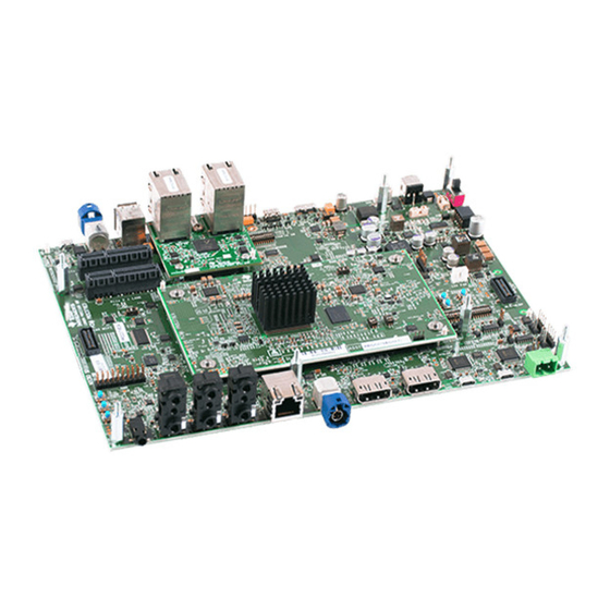
This sections provides additional details on the EVM design and processor connections. 3.1 Top Level Diagram Figure 3-1 shows the functional block diagram of the EVM Board. SPRUJ69 – DECEMBER 2022 Jacinto7 TDA4VE-Q1/TDA4VL-Q1/TDA4AL-Q1 Evaluation Module (EVM) Submit Document Feedback Copyright © 2022 Texas Instruments Incorporated... -
Page 18: Figure 3-1. Evm Functional Block Diagram
Circuit Details www.ti.com Figure 3-1. EVM Functional Block diagram Jacinto7 TDA4VE-Q1/TDA4VL-Q1/TDA4AL-Q1 Evaluation Module (EVM) SPRUJ69 – DECEMBER 2022 Submit Document Feedback Copyright © 2022 Texas Instruments Incorporated... -
Page 19: Interface Mapping
I2C0 Optional Texas Instruments, CDCI6214 SerDes Clock gen #2 I2C0 0x77,0x76 Texas Instruments, CDCI6214 Texas Instruments, CDCEL937- Peripheral Clock Gen I2C0 0x6D SPRUJ69 – DECEMBER 2022 Jacinto7 TDA4VE-Q1/TDA4VL-Q1/TDA4AL-Q1 Evaluation Module (EVM) Submit Document Feedback Copyright © 2022 Texas Instruments Incorporated... - Page 20 0x2C DS90UB926Q-Q1 Texas Instruments, PCM3168A- AUDIO IF Codec I2C3 0x44 Texas Instruments, I2C IO Expander I2C5 0x41 PCA9536DGKR Expansion, Camera I2C5 Add-On Jacinto7 TDA4VE-Q1/TDA4VL-Q1/TDA4AL-Q1 Evaluation Module (EVM) SPRUJ69 – DECEMBER 2022 Submit Document Feedback Copyright © 2022 Texas Instruments Incorporated...
-
Page 21: Gpio Mapping
‘1’ – SD Card IO Voltage is 3.3V (default) GPIO0_8 SD Card IO Voltage Selection Output Camera Expansion Board GPIO0_26 CSI2 Expansion Board Specific. Specific (Pin 18) SPRUJ69 – DECEMBER 2022 Jacinto7 TDA4VE-Q1/TDA4VL-Q1/TDA4AL-Q1 Evaluation Module (EVM) Submit Document Feedback Copyright © 2022 Texas Instruments Incorporated... - Page 22 Specific (Pin 20) (Reserved) Camera Expansion Board Camera Expansion #2 GPIO #4 Bi-Dir Specific (Pin 22) (Reserved) I2C0/TCA6416 Addr: 0x20 Function DIR/Level Remarks Jacinto7 TDA4VE-Q1/TDA4VL-Q1/TDA4AL-Q1 Evaluation Module (EVM) SPRUJ69 – DECEMBER 2022 Submit Document Feedback Copyright © 2022 Texas Instruments Incorporated...
- Page 23 0’ – External Clock is NOT enabled for PCIe1 External Clock enabled for PCIe1 Output ‘1’ – External Clock is enabled for PCIe1 (default) SPRUJ69 – DECEMBER 2022 Jacinto7 TDA4VE-Q1/TDA4VL-Q1/TDA4AL-Q1 Evaluation Module (EVM) Submit Document Feedback Copyright © 2022 Texas Instruments Incorporated...
- Page 24 Output supported) '0' - MCAN5 MCAN Interface mux selection Output '1' - Expansion/EQEP Expansion board specific (Not MDIO Mux selection Output supported) Jacinto7 TDA4VE-Q1/TDA4VL-Q1/TDA4AL-Q1 Evaluation Module (EVM) SPRUJ69 – DECEMBER 2022 Submit Document Feedback Copyright © 2022 Texas Instruments Incorporated...
- Page 25 ‘1’ – DisplayPort Power is enabled ‘0’ – DisplayPort Power is disabled (default) DisplayPort #1 Power Enable Output ‘1’ – DisplayPort Power is enabled SPRUJ69 – DECEMBER 2022 Jacinto7 TDA4VE-Q1/TDA4VL-Q1/TDA4AL-Q1 Evaluation Module (EVM) Submit Document Feedback Copyright © 2022 Texas Instruments Incorporated...
- Page 26 Peripherals at (VDD_WK_0V8 0x47 10m-ohm 0x47 3.3V 10m-ohm (VSYS_MCUIO _3V3) (VDD_CPU_AV (VSYS_IO_1V8 0x48 5m-ohm 0x48 10m-ohm (VDD_MCU_G (VSYS_IO_3V3 0x49 10m-ohm 0x49 10m-ohm PIORET_3V3) Jacinto7 TDA4VE-Q1/TDA4VL-Q1/TDA4AL-Q1 Evaluation Module (EVM) SPRUJ69 – DECEMBER 2022 Submit Document Feedback Copyright © 2022 Texas Instruments Incorporated...
- Page 27 BUILD_YR 002C / 2B (CHAR) year of production BOARDID 002E / 6B (CHAR) SERIAL_NBR 0034 / 4B (CHAR) xxxx incrementing board number SPRUJ69 – DECEMBER 2022 Jacinto7 TDA4VE-Q1/TDA4VL-Q1/TDA4AL-Q1 Evaluation Module (EVM) Submit Document Feedback Copyright © 2022 Texas Instruments Incorporated...
-
Page 28: Revision History
NOTE: Page numbers for previous revisions may differ from page numbers in the current version. DATE REVISION NOTES December 2022 Initial Release Jacinto7 TDA4VE-Q1/TDA4VL-Q1/TDA4AL-Q1 Evaluation Module (EVM) SPRUJ69 – DECEMBER 2022 Submit Document Feedback Copyright © 2022 Texas Instruments Incorporated... - Page 29 TI products. TI’s provision of these resources does not expand or otherwise alter TI’s applicable warranties or warranty disclaimers for TI products. TI objects to and rejects any additional or different terms you may have proposed. IMPORTANT NOTICE Mailing Address: Texas Instruments, Post Office Box 655303, Dallas, Texas 75265 Copyright © 2022, Texas Instruments Incorporated...
Need help?
Do you have a question about the Jacinto7 TDA4VE-Q1 and is the answer not in the manual?
Questions and answers