Table of Contents
Advertisement
Quick Links
Advertisement
Table of Contents

Related Manuals for Texas Instruments JAMR3


Summary of Contents for Texas Instruments JAMR3
- Page 1 JAMR3 User's Guide Literature Number: SPRUI52 February 2016...
-
Page 2: Table Of Contents
Portable Media and iPod ............iPod Authentication and HD Radio Conditional Access ........................ Debug Capability ..................Major Components and Connectors ......................Typical Characteristics ......................Reference Documents Table of Contents SPRUI52 – February 2016 Submit Documentation Feedback Copyright © 2016, Texas Instruments Incorporated... - Page 3 List of Figures ..................JAMR3 Application Board Top View ................JAMR3 Hardware Functional Block Diagram ................... Reset Structure Block Diagram ....................GPIO Usage Block Diagram ..................... Power Supply Block Diagram ..................Radio Functional Block Diagram ..................Audio Functional Block Diagram ..................
-
Page 4: Scope
• Audio Amplifier Interface • Interface to Jacinto 6 Processor Board In order to emulate an infotainment system, the JAMR3 board must be plugged into a required EVM CPU Board. All trademarks are the property of their respective owners. JAMR3 SPRUI52 –... -
Page 5: Overview
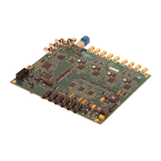
Figure 1 is an illustrative top view of the JAMR3 application board. This document only discusses the hardware for the JAMR3 application board. Details for the CPU board are not discussed in this document. Figure 1. JAMR3 Application Board Top View... - Page 6 – TVP5158 Video Decoder – 3 x AIC3106 Audio CODEC’s – 4 x AFE8310D RF2bits Tuners – 4 x AFE8316 DAB LNA’s Features and hardware functions not supported in JAMR3 application board are listed below: • Ethernet RJ45 (On Processor Board) •...
-
Page 7: Hardware
Hardware www.ti.com Hardware Application Board Hardware Architecture The JAMR3 application board block diagram is shown in Figure Radio Mini USB XR[0:1] Connector Connector Header TUNER #1 0x4B XR[2:3] TUNER #2 0x49 MSP430 XR[4:5] TUNER # 3 0x4A HDRadio XR[6:7] CA Header... -
Page 8: Processor Connector Exp_P1 Pin Assignment
IRQ2DSP_GP5[25] HDRadio CA FAULT_GP5[29] Audio Amplifier Audio Amplifier CLIP_OTW_GP5[30] Audio Amplifier Interface MUTE_EN_GP5[31] Audio Amplifier Ground Ground Ground Ground Ground Ground Ground Ground Ground Ground Unused JAMR3 SPRUI52 – February 2016 Submit Documentation Feedback Copyright © 2016, Texas Instruments Incorporated... -
Page 9: Processor Connector Exp_P2 Pin Assignment
Serial port CLK audio amp C_MCA6_AFSX Serial port FSX audio amp C_MCA6_AXR0 Audio serial port C_MCA6_AXR1 Audio serial port C_MCA6_AHCLKX Audio ref clock I2C1_SCL Tuners/LNA’s I2C1_SDA Tuners/LNA’s SPRUI52 – February 2016 JAMR3 Submit Documentation Feedback Copyright © 2016, Texas Instruments Incorporated... - Page 10 12 V DC from processor board DC_12V 12 V DC from processor board DC_12V 12 V DC from processor board DC_12V 12 V DC from processor board CPU 1.8V power supply from JAMR3 EXP_DC_1V8 board CPU 1.8V power supply from JAMR3 EXP_DC_1V8 board Power...
- Page 11 Hardware www.ti.com Table 2. Processor Connector EXP_P2 Pin Assignment (continued) Peripherals Signals Pin No Pin Count Usage/Comments Open SPRUI52 – February 2016 JAMR3 Submit Documentation Feedback Copyright © 2016, Texas Instruments Incorporated...
- Page 12 Hardware www.ti.com Table 2. Processor Connector EXP_P2 Pin Assignment (continued) Peripherals Signals Pin No Pin Count Usage/Comments Open JAMR3 SPRUI52 – February 2016 Submit Documentation Feedback Copyright © 2016, Texas Instruments Incorporated...
-
Page 13: Processor Connector Exp_P3 Pin Assignment
MMC data MMC3_DAT3 MMC data I2C2_SDA AIC3106’s, TVP5158, FPD-Link III I2C2_SCL AIC3106’s, TVP5158, FPD-Link III Ground Ground Ground Optional GND Optional Ground or Pull Down R183 Open SPRUI52 – February 2016 JAMR3 Submit Documentation Feedback Copyright © 2016, Texas Instruments Incorporated... -
Page 14: Reset Structure Block Diagram
SYS_RESETn, for the board which is qualified by the core and the I/O supplies during the power ramp cycle. The manual reset push button SW4 also generates the system reset for the JAMR3 system. When an external controller is connected, the system reset can be activated by the external controller. -
Page 15: Gpio Usage Block Diagram
1 x stereo input Battery Video SD-slot FPD-Link 2 x mono inputs Composit Functions with bold outline are for debug purpose Figure 4. GPIO Usage Block Diagram SPRUI52 – February 2016 JAMR3 Submit Documentation Feedback Copyright © 2016, Texas Instruments Incorporated... -
Page 16: Power Supply Block Diagram
Hardware www.ti.com There are seven GPIOs provided by the processor to the JAMR3 board. Table 5 summarizes the usage of the GPIOs. Table 5. GPIO Usage Summary JAMR3 Functions GPIO Ports I/O Type GPIO Usage Tuners GP6[20] RADIORST, reset radio tuner chips GP5[25] HD Radio conditional access control, interrupt to processor. -
Page 17: Quad-Tuner Radio
AM or FM. Examining pages 9 to 12 of the JAMR3 schematic shows what pads are available for this use. Connecting multiple tuners together should be done with caution and by someone that is skilled in RF engineering or the assistance of someone with RF engineering skills. - Page 18 2 GPIO signals on each DAB LNA are controlled from the processor via an I2C expander (U14, page 6 of the JAMR3 Schematic). Care must be taken when setting up the I2C expander, because MMC_WP, MMC_CD, and the video mux are also connected to this I2C expander. When changing LNA controls, care must be taken not to overwrite the state of the video mux (SEL_TVP_FPD) on the expander when the LNA states are changed.
-
Page 19: Audio Functions
Figure 6. Radio Functional Block Diagram In addition the RF input connectors, the JAMR3 board has a clock input connector, J1. The board can be modified to drive the tuner subsystem with an external reference clock instead of the crystal (X1 – see p. 9 of the schematic) attached to Tuner 1 from connector J1. -
Page 20: Audio Functional Block Diagram
A SamTec 8 pin SSW type connector (SSW-104-22-F-G-D [11]) is used for the 12 V supply. A 20-pin SFM connector (SFM-110-02-S-D-LC [12]) is utilized for the Audio Amplifier Digital Audio Connector. JAMR3 SPRUI52 – February 2016 Submit Documentation Feedback Copyright © 2016, Texas Instruments Incorporated... -
Page 21: Audio/Amp Interface Signals
SYS_RESET System reset signal from JAMR3 system The I2C#2 is the control bus that allows the processor to control and configure each codec that is an I2C slave, with the slave addresses being 0x18, 0x19 and 0x1A for AIC3106 unit #1, #2 and #3. -
Page 22: Audio Analog Signal Block Diagram
(stereo) OUT2 (CH3 OUT) Differential-to-single AIC3106’s (CH4 OUT) Outputs Differential-to-single (stereo) OUT3 (CH5 OUT) Differential-to-single ADC_OFFSET DAC_OFFSET 1.35V 1.65V Figure 8. Audio Analog Signal Block Diagram JAMR3 SPRUI52 – February 2016 Submit Documentation Feedback Copyright © 2016, Texas Instruments Incorporated... -
Page 23: Video Processing
TVP5158 or FPD-Link III outputs to the processor VDIN module. The mux is controlled by the SEL_TVP_FPD output of an I2C expander (U14, page 6 of the JAMR3 Schematic). When changing the state of the video mux, care must be taken not to change the states of the LNA controls that also emanate from the same I2C expander. -
Page 24: Portable Media And Ipod
I2C bus. FPD-Link III audio output is routed into the processor through McASP6. Portable Media and iPod A standard SD card socket is included on the JAMR3 board. SD cards (the socket may need to be placed on the PCB bottom side). - Page 25 Major Components and Connectors www.ti.com – 3.3 V Supply: U42, Texas Instruments, TPS54362-Q1 • Video: U10, Texas Instruments, TVP5158 • FPD-Link III Deserializer: U5, Texas Instruments, DS90UH926Q • USB to I2C Converter: U27, Texas Instruments, MSP430F5529IPN • Connectors – Radio – Tuner Antenna Connectors •...
-
Page 26: Typical Characteristics
Ver. 7, 7.1, 8,9,10 (2 channel audio) MPEG-4 AAC Linear PCM and MS ADPCM iPod Connection Via USB Port BACKUP CAMERA INPUTS Camera Input Connection NTSC or PAL Composite Video JAMR3 SPRUI52 – February 2016 Submit Documentation Feedback Copyright © 2016, Texas Instruments Incorporated... -
Page 27: Reference Documents
17. JAMR3 Tuner EVM Application Board Schematic Rev B (SPRR215) 18. JAMR3 Tuner EVM Application Board BOM Rev B (SPRR216) 19. JAMR3 Tuner EVM Application Board CPU Assembly Drawing Rev B (SPRR217) 20. JAMR3 Tuner EVM Application Board CPU PCB Drawing Rev B (SPRR218) SPRUI52 –... - Page 28 STANDARD TERMS AND CONDITIONS FOR EVALUATION MODULES Delivery: TI delivers TI evaluation boards, kits, or modules, including any accompanying demonstration software, components, or documentation (collectively, an “EVM” or “EVMs”) to the User (“User”) in accordance with the terms and conditions set forth herein. Acceptance of the EVM is expressly subject to the following terms and conditions.
- Page 29 FCC Interference Statement for Class B EVM devices NOTE: This equipment has been tested and found to comply with the limits for a Class B digital device, pursuant to part 15 of the FCC Rules. These limits are designed to provide reasonable protection against harmful interference in a residential installation.
- Page 30 【無線電波を送信する製品の開発キットをお使いになる際の注意事項】 開発キットの中には技術基準適合証明を受けて いないものがあります。 技術適合証明を受けていないもののご使用に際しては、電波法遵守のため、以下のいずれかの 措置を取っていただく必要がありますのでご注意ください。 1. 電波法施行規則第6条第1項第1号に基づく平成18年3月28日総務省告示第173号で定められた電波暗室等の試験設備でご使用 いただく。 2. 実験局の免許を取得後ご使用いただく。 3. 技術基準適合証明を取得後ご使用いただく。 なお、本製品は、上記の「ご使用にあたっての注意」を譲渡先、移転先に通知しない限り、譲渡、移転できないものとします。 上記を遵守頂けない場合は、電波法の罰則が適用される可能性があることをご留意ください。 日本テキサス・イ ンスツルメンツ株式会社 東京都新宿区西新宿6丁目24番1号 西新宿三井ビル 3.3.3 Notice for EVMs for Power Line Communication: Please see http://www.tij.co.jp/lsds/ti_ja/general/eStore/notice_02.page 電力線搬送波通信についての開発キットをお使いになる際の注意事項については、次のところをご覧くださ い。http://www.tij.co.jp/lsds/ti_ja/general/eStore/notice_02.page SPACER EVM Use Restrictions and Warnings: 4.1 EVMS ARE NOT FOR USE IN FUNCTIONAL SAFETY AND/OR SAFETY CRITICAL EVALUATIONS, INCLUDING BUT NOT LIMITED TO EVALUATIONS OF LIFE SUPPORT APPLICATIONS.
- Page 31 Notwithstanding the foregoing, any judgment may be enforced in any United States or foreign court, and TI may seek injunctive relief in any United States or foreign court. Mailing Address: Texas Instruments, Post Office Box 655303, Dallas, Texas 75265 Copyright © 2015, Texas Instruments Incorporated...
- Page 32 IMPORTANT NOTICE Texas Instruments Incorporated and its subsidiaries (TI) reserve the right to make corrections, enhancements, improvements and other changes to its semiconductor products and services per JESD46, latest issue, and to discontinue any product or service per JESD48, latest issue.
Need help?
Do you have a question about the JAMR3 and is the answer not in the manual?
Questions and answers