Sign In
Upload
Manuals
Brands
Texas Instruments Manuals
Motherboard
Jacinto7 J721E
Texas Instruments Jacinto7 J721E Manuals
Manuals and User Guides for Texas Instruments Jacinto7 J721E. We have
1
Texas Instruments Jacinto7 J721E manual available for free PDF download: User Manual
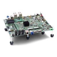
Texas Instruments Jacinto7 J721E User Manual (85 pages)
DRA829/TDA4VM Evaluation Module
Brand:
Texas Instruments
| Category:
Motherboard
| Size: 7 MB
Table of Contents
Table of Contents
1
Introduction
5
Key Features
5
Thermal Compliance
6
Thermal Caution
6
REACH Compliance
7
J721E EVM Board
7
J721E EVM Overview
7
System Architecture Interface
8
J721E EVM Board Identification
9
J721E EVM Board Identification (SOM, CPB, QP Ethernet)
9
J721E SOM Component Identification
10
Jacinto7 Common Processor Components Identification
11
Jacinto7 Common Processor Component Identification
11
Quad Ethernet Components Identification
12
Quad Ethernet Component Identification
12
EVM User Setup/Configuration
13
Power Requirements
13
Connector Used for Power Input
13
Recommended External Power Supply
13
Power on Switch and Power Leds
14
Power ON/OFF Switch
14
Power On/Fault Leds
15
Power LED Status
15
Power Status Leds
16
Power Leds
16
Power Test Points
17
EVM Reset/Interrupt Push Buttons
18
EVM Push Buttons
18
EVM DIP Switches
19
EVM Configuration DIP Switch
19
EVM Configuration Switch Function
20
EVM Configuration Switch Function
21
BOOT Switches Provided on the Processor Card
22
Wakup Boot Mode Switch (SW9)
22
Main Boot Mode Switch (SW8)
22
EVM UART/COM Port Mapping
23
UART Port Mapping
23
JTAG Emulation
24
JTAG Mux
24
JTAG 1:2 Mux Selection
24
TI 60 Pin Connector (J16) Pinout
25
Cti20 Pin Connector (J1-Refer PROC081E2 SCH) Pinout
26
TI14 Pin Connector (J2-Refer PROC081E2 SCH) Pinout
26
J721E EVM Hardware Architecture
27
J721E EVM Hardware Top Level Diagram
27
J721E EVM Functional Block Diagram
27
Quad Port Ethernet Expansion Functional Block Diagram
28
J721E EVM Interface Mapping
29
I2C Address Mapping
30
J721E EVM I2C Table
30
GPIO Mapping
31
J721E Soc - GPIO Mapping Table
31
Power Supply
32
J721E SOM Power Distribution Block Diagram
32
Power on Sequencing
33
Voltage Supervisor Circuit
34
LPDDR4 IO Voltage Selection Circuit
35
DDR I/O Voltage Selection
35
J721E Soc S2R Logic Flow
36
INA Devices I2C Slave Address
37
Reset
38
External Power Monitor Header Pinouts
38
EVM Reset Architecture
39
Clock
40
EVM Clock Architecture
40
J721E Soc Primary Clock
41
Processor's Secondary/Serdes Ref Clock
42
EVM Peripheral Ref Clock
42
Memory Interfaces
43
J721E Som LPDDR4
43
J721E Som OSPI and Hyper Flash
44
UFS Memory Block Diagram
45
Emmc Memory Block Diagram
46
Micro-SD Card Block Diagram
47
Board ID Memory Header Information
48
MCU Ethernet Interface
49
MCU Gigabit Ethernet Block
49
MCU Ethernet PHY Settings
50
4.10 QSGMII Ethernet Interface
51
Clock Source Selection
51
Quad-SGMII Board I2C
52
4.11 Pcie Interface
53
QSGMII Ethernet PHY Settings
53
Pcie Interface for SERDES0
54
Pcie SMBUS Block Diagram
54
Reference Clock Selection for Pcie Host Operation
55
Reference Clock Selection for Pcie Endpoint Operation
55
USB2.0 Header Connection
56
Resistors for Selecting Pcie Card Host or Device Operation
56
Pcie Interface for SERDES1
57
Resistors for Selecting Pcie Card Host or Device Operation
58
4.12 USB Interface
59
Reference Clock Selection for Pcie Host Operation
58
Reference Clock Selection for Pcie Endpoint Operation
58
Pcie Interface for SERDES2
59
USB3.1 Type C Interface
60
Type C Power Delivery Current Settings
60
USB Hub Reference Clock Circuit
61
USB Hub Settings Circuit
61
USB1 ID Setting for HUB
61
4.13 CAN Interface
62
MCU CAN0 Interface
62
CAN Wake Push Button
63
CAN Header Connections to Db9/Test Instrument
64
FPD Interface (Audio Deserializer)
65
FPD-Link UB926 ID Setting Circuit
65
FPD-Link UB926 Mode Selection Circuit
65
FPD Panel Interface (DSI Video Serializer)
66
FPD Audio Deserializer HSD Connector Pinout
66
DSI to FPD Serializer HSD Connector Pinout
66
4.16 Display Serial Interface (DSI) FPC
67
4.17 Audio Interface
67
FPD-Link UB981 Device Settings Circuit
66
MCASP/TRACE - 1:3 MUX: Truth Table
67
Config Table
67
Audio Port Interface Assignment
68
4.18 Display Port Interface
69
4.19 MLB Interface
69
Display Port Block Diagram
69
MLB Header Pinout
70
4.20 I3C Interface
71
4.21 ADC Interface
71
MLB Interface Connector
70
MCU I3C Header J33 Pinout
71
MAIN I3C Header J32 Pinout
71
4.22 RTC Interface
72
ADC Interface Connector
71
ADC Header J23 Pinout
72
4.23 Apple Authentication Header
73
RTC Block Diagram
72
APPLE AUTH Header J9 Pinout
73
Apple Authentication Block Diagram
73
4.24 EVM Expansion Connectors
74
APPLE AUTH Footprint U108 Pinout
74
Expansion Board Interface Connectors
74
EVM Expansion Connector J46 Pinout
75
EVM Expansion Connector J51 Pinout
77
4.25 ENET Expansion Connector
78
ENET Expansion Board Power Test Points
78
CDCI I2C Isolation Circuit
79
ENET Expansion Connector J10 Pinout
80
4.26 CSI Expansion Connector
82
Dual I/O Voltage Selection for CSI Expansion Interface
82
CSI Expansion Connector J52 Pinout
83
CSI Expansion Connector J48 Pinout
83
Advertisement
Advertisement
Related Products
Texas Instruments J721EXSOMXEVM
Texas Instruments J7EXPCXEVM
Texas Instruments J721EXCPXEVM
Texas Instruments TSW14J58 JESD204C
Texas Instruments J721E
Texas Instruments JAMR3
Texas Instruments J722SXH01
Texas Instruments J722SXH01EVM
Texas Instruments J742S2XH01EVM
Texas Instruments JESD204B
Texas Instruments Categories
Motherboard
Control Unit
Microcontrollers
Computer Hardware
Calculator
More Texas Instruments Manuals
Login
Sign In
OR
Sign in with Facebook
Sign in with Google
Upload manual
Upload from disk
Upload from URL