Advertisement
NXP Semiconductors
User's Guide
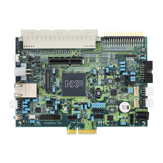
MPC5777C EVB User Guide
Prototype Board
by: NXP Semiconductors
1.
Introduction
This user guide details the setup and configuration
of the NXP MPC5777C Evaluation Board
(hereafter referred to as the EVB). The EVB is
intended to provide a mechanism for easy
customer evaluation of the MPC57xx family of
microprocessors, and to facilitate hardware and
software development.
At the time of writing this document, the
MPC57xx
family
powertrain and safety devices. For the latest
product information, please speak to your NXP
representative or consult the MPC57xx website at
www.nxp.com
The EVB is intended for bench or laboratory use
and has been designed using normal temperature
specified components (+70°C).
consists
of
the
55nm
Contents
1.
Introduction ..................................................................... 1
2.
EVB Features ................................................................. 2
Configuration - Motherboard ........................................ 3
3.
4.
5.
6.
Board Interface Connector ........................................... 41
7.
Default Jumper Summary Table ................................... 55
8.
List of Acronyms ........................................................... 58
Document Number:
MPC5777CEVBUG
Rev. 1, 03/2019
Advertisement

Related Manuals for NXP Semiconductors MPC5777C


Summary of Contents for NXP Semiconductors MPC5777C
-
Page 1: Table Of Contents
(hereafter referred to as the EVB). The EVB is Configuration — Motherboard ........3 intended to provide a mechanism for easy Configuration — MPC5777C-416DS Daughter card ..13 customer evaluation of the MPC57xx family of Configuration — MPC5777C-516DS Daughter card ..27 microprocessors, and to facilitate hardware and Board Interface Connector ........... -
Page 2: Evb Features
A number of compatible daughter cards are available for the motherboard across a number of devices. Table 1 gives an overview of daughter cards that can be used with MPC57xx motherboard (Part Number: MPC57XXXMB) and associated MPC5777C devices, package sizes and part numbers. Table 1: Daughter Card Overview Daughter card number... -
Page 3: Configuration - Motherboard
4 user switches and 4 user LEDs, freely connectable • Liberal scattering of GND test points (surface mount loops) placed throughout the EVB **Mother Board has FlexRAY connector, but this feature is not used on MPC5777C The daughter cards provide the following features: •... - Page 4 There is also a power supply option on the daughter card to use the daughter card in standalone Section 4.1.2, 4.1.3 “Daughter Card Standalone Power Input -External & mode. Please refer to Daughter Card Standalone Power Input –Power SBC” for details on the daughter card power input. MPC5777C EVB User Guide, Rev. 1 NXP Semiconductors...
- Page 5 Disconnecting J60 enables the 1.25 V switching regulator The regulators supply power to the daughter cards through the board connector. The individual selection and configuration of the MCU supplies are done on the daughter cards. MPC5777C EVB User Guide, Rev. 1 NXP Semiconductors...
- Page 6 The EVB has two NXP TJA1041T high speed CAN transceivers and two standard DB9 connectors to provide physical CAN interfaces for the MCU. The pinout of the DB9 connectors (J5/J6) is shown in Figure 5. Figure 5: CAN DB9 connector Pin out MPC5777C EVB User Guide, Rev. 1 NXP Semiconductors...
- Page 7 PHY U1 TX to MCU 1-2: MCAN1 TX 2-3: TTCAN TX PHY U1 RX to MCU — 1-2: MCAN1 RX 2-3: TTCAN RX PHY U1 signal out — 1: ERR 2: INH MPC5777C EVB User Guide, Rev. 1 NXP Semiconductors...
- Page 8 The EVB is fitted with a NXP MC33662LEF LIN transceiver (U50) and two different style connectors: A standard LIN Molex connector (J4) at the edge of the board and a standard 0.1 in. connector (P3). The pin-out of the Molex connector J4 is shown in Figure MPC5777C EVB User Guide, Rev. 1 NXP Semiconductors...
- Page 9 LIN transceiver power input to pin2. This allows the LIN transceiver to be powered directly from the EVB supply by simply linking pins 1 and 2 of connector P3 using a 0.1 in. jumper shunt. Figure 9: LIN 4pin header interface connector MPC5777C EVB User Guide, Rev. 1 NXP Semiconductors...
- Page 10 Power from all the three switching regulators is readily accessible along with GND through JP1 – JP16 next to the prototyping area. This area is ideal for the addition of any custom circuitry. MPC5777C EVB User Guide, Rev. 1 NXP Semiconductors...
- Page 11 Hook Ground reference Hook Ground reference Hook Ground reference Hook Ground reference Hook Ground reference Hook Ground reference Hook Ground reference GT10 Hook Ground reference GT11 Hook Ground reference 1.25V_SR 1.25V_SR reference MPC5777C EVB User Guide, Rev. 1 NXP Semiconductors...
- Page 12 Ground reference 5V_SR TP15 Hook 5V_SR reference 5V_LR TP14 Hook 5V_LR reference 3.3V_SR TP16 Hook 3.3V_SR reference 1.25V_SR TP17 Hook 1.25V_SR reference FRA-INH2 Unused FRA-INH1 Unused FRA-ERRN Unused FRA-RXEN Unused FRB-INH2 Unused MPC5777C EVB User Guide, Rev. 1 NXP Semiconductors...
-
Page 13: Configuration - Mpc5777C-416Ds Daughter Card
FEC 25MHz clock Configuration — MPC5777C-416DS Daughter card This section details the configuration of each of the MPC5777C-416DS daughter card’s functional blocks. The daughter card has been designed with ease of use in mind and has been segmented into functional... - Page 14 Board Interface Connector Figure 10: MPC5777C-416DS Daughter card — functional blocks MCU Power 4.1.1 Supply Routing and Jumpers The different MCU supplies are connected to the regulators on the Mother Board through the interface connector. Also daughter card has option to connect MCU supplies to either Mother Board supplies or onboard regulators.
- Page 15 Board Interface Connector Figure 11: Daughter card power distribution Available power supply modes of MPC577C are listed in Table 7 Table 7: Power modes of MPC5777C 1.2V Mode 3.3V Flash VDDPMC&V Configuration Regulator REGSEL VDDFLA Name Supply DDPWR controller Internal 3.3V Flash regulator with...
- Page 16 J9 & J10 J10, 1-2: Connect VRH_EQ* VRH_EQ CAUTION: For 1.25 V source selection, a single jumper must be installed on either J21 or J12, but not on both at a time. MPC5777C EVB User Guide, Rev. 1 NXP Semiconductors...
- Page 17 1-2: Select 3.3V* JTAG IO Level - VDD_HV_IO_JTAG 2-3: Select 5V J520 Connect LED for ETPUA0 1-2: Connect LED with Signal ETPUA0* J521 Connect LED for ETPUA1 1-2: Connect LED with Signal ETPUA1* MPC5777C EVB User Guide, Rev. 1 NXP Semiconductors...
- Page 18 • LIN Transceiver • Debug Mode Power Switch SW1 should be in ON position to use Daughter card in standalone mode which enables the use Power SBC supplies to MCU power domain. MPC5777C EVB User Guide, Rev. 1 NXP Semiconductors...
- Page 19 Power SBC has High Speed CAN Transceiver & LIN Transceiver. CAN bus from SBC is terminated with DB9 connector (J508) and LIN is terminated with 4-pin Molex connector (J503) in the Daughter Card. The connections of the J508 (CAN) from PowerSBC are detailed in Figure 13. MPC5777C EVB User Guide, Rev. 1 NXP Semiconductors...
- Page 20 8-9, 11-12: Select LIN from Mother Board* CAN/LIN Selection J506 SBC/ Mother Board 1-2, 4-5 : Select CAN from PowerSBC 7-8, 10-11: Select LIN from PowerSBC 1-3: Enable CANL Termination* J507 CAN Termination 2-4: Enable CANH Termination* MPC5777C EVB User Guide, Rev. 1 NXP Semiconductors...
- Page 21 In addition to the internal 16 MHz oscillator, the MCU can also be clocked by external oscillator (Y1). The clock circuitry for the 40 MHz crystal is shown in Figure 15. Figure 15: 40 MHz crystal circuit MPC5777C EVB User Guide, Rev. 1 NXP Semiconductors...
- Page 22 JTAG Power 2-3: Connect 5.0V to VDD_HV_IO_JTAG Figure 16: JTAG connector point Nexus Connector Table 14 Shows the pinout of the 50-pin SAMTEC connector for the MPC5777C (emulation device) Table 14: Trace Connector Pinout Pin No Function Pin No Function MSEO0_B 3.3V_SR...
- Page 23 The signals from the MCU’s Fast Ethernet Controller are terminated to Mother Board interface connector, J501. Further these signals are connected with Ethernet Physical Interface in the Mother Board. Also, in order to support Reduced Media-Independent Interface (RMII) mode, the Daughter MPC5777C EVB User Guide, Rev. 1 NXP Semiconductors...
- Page 24 • a clock. The clock is unidirectional and is defined to be an output on the Slave and an input on the Master node. The daughter card SIPI connector (J13) interface signal diagram is shown in Figure 19. MPC5777C EVB User Guide, Rev. 1 NXP Semiconductors...
- Page 25 Enhanced Modular IO Subsystem (eMIOS) • Enhanced Time Processing Unit (eTPU) • Deserial Serial Peripheral Interface (DSPI) 4.10 Test points — 416 Daughter Card MPC5777C-416DS Daughter card test points are listed and detailed in Table 17 MPC5777C EVB User Guide, Rev. 1 NXP Semiconductors...
- Page 26 TP27 SBC_5V GT1 to GT11 Hook Ground Reference 5.0V_SR 5.0V Switching Regulator Ground Reference 3.3V_SR 3.3V Switching Regulator 5.0V_SR 5.0V Switching Regulator 1.25V_SR 1.25V Switching Regulator Ground Reference 3.3V_SR 3.3V Switching Regulator MPC5777C EVB User Guide, Rev. 1 NXP Semiconductors...
-
Page 27: Configuration - Mpc5777C-516Ds Daughter Card
J5 (2-3) (5.0V_SR) to Analog Supply Rail. Configuration — MPC5777C-516DS Daughter card This section details the configuration of each of the MPC5777C-516DS daughter card’s functional blocks. The daughter card has been designed with ease of use in mind and has been segmented into functional blocks as shown in . - Page 28 Board Interface Connector Figure 20: MPC5777C-516DS Daughter card — functional blocks MCU Power 5.1.1 Supply Routing and Jumpers The different MCU supplies are connected to the regulators on the Mother Board through the interface connector. Also daughter card has option to connect MCU supplies to either Mother Board supplies or onboard regulators.
- Page 29 Fast I/O Pads supply selection - 1-2: Select 3.3V* VDDE2 2-3: Select 5V CAUTION: For 1.25 V source selection, a single jumper must be installed on either J513 or J13, but not on both at a time. MPC5777C EVB User Guide, Rev. 1 NXP Semiconductors...
- Page 30 2-3: Select 5 V J520 Connect LED for ETPUA0 1-2: Connect LED with Signal ETPUA0* J521 Connect LED for ETPUA1 1-2: Connect LED with Signal ETPUA1* 2-3: For 5 V VDD_HV_IO_MAIN_SEL 1-2: For 3.3 V MPC5777C EVB User Guide, Rev. 1 NXP Semiconductors...
- Page 31 • LIN Transceiver • Debug Mode Power Switch SW1 should be in ON position to use Daughter card in standalone mode which enables the use Power SBC supplies to MCU power domain. MPC5777C EVB User Guide, Rev. 1 NXP Semiconductors...
- Page 32 Power SBC has High Speed CAN Transceiver & LIN Transceiver. CAN bus from SBC is terminated with DB9 connector (J508) and LIN is terminated with 4-pin Molex connector (J503) in the Daughter Card. The connections of the J508 (CAN) from PowerSBC are detailed in Figure 22. MPC5777C EVB User Guide, Rev. 1 NXP Semiconductors...
- Page 33 8-9, 11-12: Select LIN from Mother Board* CAN/LIN Selection J506 SBC/ Mother Board 1-2, 4-5 : Select CAN from PowerSBC 7-8, 10-11: Select LIN from PowerSBC 1-3: Enable CANL Termination* J507 CAN Termination 2-4: Enable CANH Termination* MPC5777C EVB User Guide, Rev. 1 NXP Semiconductors...
- Page 34 In addition to the internal 16 MHz oscillator, the MCU can also be clocked by external oscillator (Y1). The clock circuitry for the 40 MHz crystal is shown in Figure Figure 24: 40 MHz crystal circuit MPC5777C EVB User Guide, Rev. 1 NXP Semiconductors...
- Page 35 Jumper Setting 1-2: Connect 3.3V to VDD_HV_IO_JTAG JTAG Power 2-3: Connect 5.0V to VDD_HV_IO_JTAG Nexus Connector Table Shows the pinout of the 50-pin SAMTEC connector for the MPC5777C (emulation device) Table 24: Trace Connector Pinout Pin No Function Pin No Function MSEO0_B 3.3V_SR...
- Page 36 The signals from the MCU’s Fast Ethernet Controller are terminated to Mother Board interface connector, J501. Further these signals are connected with Ethernet Physical Interface in the Mother Board. Also, in order to support Reduced Media-Independent Interface (RMII) mode, the Daughter MPC5777C EVB User Guide, Rev. 1 NXP Semiconductors...
- Page 37 External Bus Interface (EBI) is not available on 416 BGA. It is available only on the 516 BGA. The EBI is interfaced with Cypress’ 4Mbit SRAM on MPC5777C-516DS Daughter Card as shown J4 allows connection of SRAM’s chip select with MCU ship select D_CS0 or Figure 27 D_CS1.
- Page 38 • a clock. The clock is unidirectional and is defined to be an output on the Slave and an input on the Master node. The daughter card SIPI connector (J14) interface signal diagram is shown in Figure 28. MPC5777C EVB User Guide, Rev. 1 NXP Semiconductors...
- Page 39 Enhanced Modular IO Subsystem (eMIOS) • Enhanced Time Processing Unit (eTPU) • Deserial Serial Peripheral Interface (DSPI) 5.11 Test points — 516 Daughter Card MPC5777C-516DS Daughter card test points are listed and detailed in Table MPC5777C EVB User Guide, Rev. 1 NXP Semiconductors...
- Page 40 TP31 SBC_5V GT1 to GT11 Hook Ground Reference 5.0V_SR 5.0V Switching Regulator Ground Reference 3.3V_SR 3.3V Switching Regulator 5.0V_SR 5.0V Switching Regulator 1.25V_SR 1.25V Switching Regulator Ground Reference 3.3V_SR 3.3V Switching Regulator MPC5777C EVB User Guide, Rev. 1 NXP Semiconductors...
-
Page 41: Board Interface Connector
• Ground signals are not listed here. A solid ground connection is achieved through the middle bar of the interface connector. MPC5777C EVB User Guide, Rev. 1 NXP Semiconductors... - Page 42 CNTXB PA10 CNRXB PA11 PA12 PA13 TP26/TP22 PA14 CLK_50MHz_B PA15 5.0V_SR_MB 5.0V_SR 5.0V_SR_MB 5.0V_SR 5.0V_SR_MB 5.0V_SR 5.0V_SR_MB 5.0V_SR BOOTCFG0 PCSA3 PCSB4 WKPCFG PLLCFG1 BOOTCFG1 PLLCFG2 MB_CAN_RXD MB_CAN_TXD PCSA4 PC10 PC11 FEC_RDX0 PC12 MPC5777C EVB User Guide, Rev. 1 NXP Semiconductors...
- Page 43 3.3_SR_MB 3.3V_SR 3.3_SR_MB 3.3V_SR 3.3_SR_MB 3.3V_SR 3.3_SR_MB 3.3V_SR CNTXD MB_LIN_RXD MB_LIN_TXD PE10 PE11 FEC_TXD1 PE12 PE13 PE14 PE15 1.25V_SR_MB 1.25V_SR 1.25V_SR_MB 1.25V_SR 1.25V_SR_MB 1.25V_SR 1.25V_SR_MB 1.25V_SR CNRXC CNTXC PG10 PG11 PG12 PG13 MPC5777C EVB User Guide, Rev. 1 NXP Semiconductors...
- Page 44 EMIOS11 PI10 EMIOS12 PI11 EMIOS13 PI12 EMIOS14 PI13 EMIOS15 PI14 EMIOS16 PI15 EMIOS17 EMIOS18 EMIOS19 EMIOS20 EMISO21 EMIOS22 EMIOS23 EMIOS24 EMIOS25 EMIOS26 EMIOS27 PK10 EMIOS28 PK11 EMIOS29 PK12 EMIOS30 PK13 PK_14 PK14 MPC5777C EVB User Guide, Rev. 1 NXP Semiconductors...
- Page 45 PCSB0 PM10 PCSB3 PM11 EMIOS31 PM12 PCSA0 PM13 PLLCFG0 PM14 SINB PM15 RST-SW_B RST-SW VDD_HV_IO_FLEX VDD_HV_IO_FLEX VDD_HV_IO_FLEX SCKB PCSC0 SOUTB PCSC2 PCSC1 PCSC4 PCSC3 SCKC PCSC5 SOUTC SINC PO10 PO11 PO12 PO13 MPC5777C EVB User Guide, Rev. 1 NXP Semiconductors...
- Page 46 ANA15 PQ14 ANA16_SDB0 PQ15 5.0_SR_MB 5.0V_SR 5.0_SR_MB 5.0V_SR 5.0_SR_MB 5.0V_SR 5.0_SR_MB 5.0V_SR ANA17_SDB1 ANA18_SDB2 ANA19_SDB3 ANA20_SDC0 ANA21_SDC1 ANA22_SDC2 ANA23_SDC3 AN24 AN25 AN26 AN27 PS10 AN28 PS11 AN29 PS12 AN30 PS13 AN31 PS14 MPC5777C EVB User Guide, Rev. 1 NXP Semiconductors...
- Page 47 ANB8 PU15 VDD_HV_IO_MAIN VDD_HV_IO_MAIN VDD_HV_IO_MAIN VDD_HV_IO_MAIN VDD_HV_IO_MAIN VDD_HV_IO_MAIN VDD_HV_IO_MAIN VDD_HV_IO_MAIN ANB9 ANB10 ANB11 ANB12 ANB13 ANB14 ANB15 ANB16 ANB17 ANB18 ANB19 PW10 ANB20 PW11 ANB21 PW12 ANB22 PW13 ANB23 PW14 SENT2_A PW15 MPC5777C EVB User Guide, Rev. 1 NXP Semiconductors...
- Page 48 ETPUA11 PN10 ETPUA10 PN11 ETPUA13 PN12 ETPUA12 PN13 ETPUA15 PN14 ETPUA14 PN15 ETPUA17 ETPUA16 ETPUA19 ETPUA18 ETPUA21 ETPUA20 ETPUA23 ETPUA22 ETPUA25 ETPUA24 ETPUA27 PP10 ETPUA26 PP11 ETPUA29 PP12 ETPUA28 PP13 ETPUA31 PP14 MPC5777C EVB User Guide, Rev. 1 NXP Semiconductors...
- Page 49 ETPUB14 PR15 5.0V_SR_MB 5.0V_SR 5.0V_SR_MB 5.0V_SR 5.0V_SR_MB 5.0V_SR 5.0V_SR_MB 5.0V_SR ETPUB17 ETPUB16 ETPUB19 ETPUB18 ETPUB21 ETPUB20 ETPUB23 ETPUB22 ETPUB25 ETPUB24 ETPUB27 PT10 ETPUB26 PT11 ETPUB29 PT12 ETPUB28 PT13 ETPUB31 PT14 ETPUB30 PT15 MPC5777C EVB User Guide, Rev. 1 NXP Semiconductors...
- Page 50 ETPUC14 PV15 VDD_HV_IO_MAIN VDD_HV_IO_MAIN VDD_HV_IO_MAIN VDD_HV_IO_MAIN VDD_HV_IO_MAIN VDD_HV_IO_MAIN VDD_HV_IO_MAIN VDD_HV_IO_MAIN ETPUC17 ETPUC16 ETPUC19 ETPUC18 ETPUC21 ETPUC20 ETPUC23 ETPUC22 ETPUC25 ETPUC24 ETPUC27 PX10 ETPUC26 PX11 ETPUC29 PX12 ETPUC28 PX13 ETPUC31 PX14 ETPUC30 PX15 MPC5777C EVB User Guide, Rev. 1 NXP Semiconductors...
- Page 51 1.25V_SR_MB 1.25_SR 1.25V_SR_MB 1.25_SR 1.25V_SR_MB 1.25_SR 1.25V_SR_MB 1.25_SR PB10 PB11 PB12 PB13 PB14 PB15 5.0V_SR_MB 5.0V_SR 5.0V_SR_MB 5.0V_SR 5.0V_SR_MB 5.0V_SR 5.0V_SR_MB 5.0V_SR D_CS3 TP11 TP10/TP9 D_TA PD10 PD11 PD12 PD13 TXDC PD14 MPC5777C EVB User Guide, Rev. 1 NXP Semiconductors...
- Page 52 Port RXDC PD15 3.3V_SR_MB 3.3V_SR 3.3V_SR_MB 3.3V_SR 3.3V_SR_MB 3.3V_SR 3.3V_SR_MB 3.3V_SR PF10 PF11 PF12 TP8/TP10 PF13 PF14 PF15 1.25V_SR_MB 1.25V_SR 1.25V_SR_MB 1.25V_SR 1.25V_SR_MB 1.25V_SR 1.25V_SR_MB 1.25V_SR PH10 PH11 PH12 PH13 PH14 PH15 MPC5777C EVB User Guide, Rev. 1 NXP Semiconductors...
- Page 53 Evaluation Board mP Pin Name(516/416) Connector Pin # Connector Pin # Port 3.3V_SR_MB 3.3V_SR 3.3V_SR_MB 3.3V_SR 3.3V_SR_MB 3.3V_SR 3.3V_SR_MB 3.3V_SR TP9/TP8 PJ10 PJ11 PJ12 PJ13 PJ14 PJ15 PL10 PL11 PL12 PL13 PL14 PL15 MPC5777C EVB User Guide, Rev. 1 NXP Semiconductors...
- Page 54 Nexus TX0N PL15 Nexus TX0P PA14 SIPI_TXP Nexus EVTI0 SIPI_TXN Nexus EVTO0 SIPI_RXP Nexus EVTO1 — PF13 SIPI_RXN Nexus TX2N — Nexus CLKP Nexus TX2P — Nexus CLKN Nexus TX3N — Nexus TX3P MPC5777C EVB User Guide, Rev. 1 NXP Semiconductors...
-
Page 55: Default Jumper Summary Table
1-2: Ethernet signal: RXER_MDIXEN SCI-PWR 1-2: SCI PHY power-on — 1-2: Ethernet signal: RXDV_MIIMODE 1-2: PHY U4 TX to MCU 3-4: PHY U4 TXEN to MCU FR-A 5-6: PHY U4 RX to MCU MPC5777C EVB User Guide, Rev. 1 NXP Semiconductors... - Page 56 — Ethernet signal: RXD1_PHYAD1 — Ethernet signal: RXD2_PHYAD2 — Ethernet signal: RXD3_PHYAD3 — Ethernet signal: COL_PHYAD0 — Ethernet signal: TXEN — Ethernet signal: TXCLK — Ethernet signal: TXD0 — Ethernet signal: TXD1 MPC5777C EVB User Guide, Rev. 1 NXP Semiconductors...
- Page 57 DISABLE Disable 1.25V switching regulator Disable 3.3V switching regulator DISABLE DISABLE Disable 5.0V switching regulator — 1-2: PM0 to GND — 1-2: RST-SW — 1-2 : QZ1-X1 connect — 1-2: QZ1-X2 connect MPC5777C EVB User Guide, Rev. 1 NXP Semiconductors...
-
Page 58: List Of Acronyms
P12V 12 V EVB supply power domain Printed Circuit Board PORST Power-on reset Power RMII Reduced Media-Independent Interface Receive System Basis Chip To be defined Test Point Transmit Universal Serial Bus Ground MPC5777C EVB User Guide, Rev. 1 NXP Semiconductors... - Page 59 Information in this document is provided solely to enable system and software How to Reach Us: implementers to use NXP products. There are no express or implied copyright licenses Home Page: granted hereunder to design or fabricate any integrated circuits based on the nxp.com information in this document.
- Page 60 Mouser Electronics Authorized Distributor Click to View Pricing, Inventory, Delivery & Lifecycle Information: MPC5775BE-416DS MPC5777C-416DS MPC5777C-516DS...
Need help?
Do you have a question about the MPC5777C and is the answer not in the manual?
Questions and answers