Table of Contents
Advertisement
Advertisement
Table of Contents

Related Manuals for Strong SRT8500


Summary of Contents for Strong SRT8500
- Page 1 service manual DTT1609...
-
Page 2: Table Of Contents
CONTENTS 1 MAIN BOARD TROUBLE SHOOTING GUIDE 1.1 SHORT TEST 1.2 POWER 1.3 MAIN CLOCK 1.4 CVBS 1.5 RGB 1.6 AUDIO # ADDITIONAL TROUBLESOOTHING 2 SCHEMATIC.COMPONENT LAYOUT AND BOM OF POWER SUPPLY 2.1 SCHEMATIC OF POWER SUPPLY 2.2 COMPONENT LAYOUT OF POWER SUPPLY 3 SCHEMATIC.COMPONENT LAYOUT AND BOM OF MAIN BOARD 3.1 SCHEMATIC OF MAIN BOARD 3.2 COMPONENT LAYOUT OF MAIN BOARD... -
Page 3: Main Board Trouble Shooting Guide
Main Board Main Board Trouble Shooting Guide (DTT1609) Here are the procedures you can refer to whenever terrestrial receivers do not operate properly. You can check problems and repair the units on the basic level according to the following procedures... -
Page 4: Short Test
1. SHORT TEST ☞Before turning on AC power, check POSITIVE VOLTAGE and also check whether SHORT between GROUND's and PIN SHORT for TUNER are detected or not. 2. Checking POWER. +12V(SCART),+5V(ANTENNA_POWER,IR,VIDEO BUFFER,HDMI,USB), +3.3V(TUNER, FLASH, ☞ CPU),+2.5V(DEMOD),+1.5V(DDR3,CPU),+1.3V(CPU DEMOD) - Page 5 +12V +5V For HDMI +3V3 For Tuner...
- Page 6 +3V3 +3V3 For Cpu +1V3 For +1V5 For Cpu +1V5 For DDR3...
- Page 7 +2V5 For DEMOD +1V3 For DEMOD +5V For +5V For Video Buffer +5V For Audio...
- Page 8 3. Check MAIN CLOCK 24MHz and SYSTEM CLOCK (PLL) to operate normally after SYSTEM operates. For the first thing, check 24MHz from Y401 flows into [OSCI(PIN B18)] of MAIN ☞ If the 24MHz is unstable, Check Y401 is damaged or not. If you are firm belief of damage for the device, then replace the device.
-
Page 9: Main Clock
MAIN CLOCK DDR3 CLOCK 800Mhz... - Page 10 4. In case that MAIN CPU operates normally but there is no VIDEO display. In case of no OSD display. ▶ If OSD is not displayed, check first if VIDEO SIGNAL is detected from ☞ [R419(CVBS),R416(R),R417(G),R418(B)] of MAIN CPU. And then, check any part with no DATA after checking VIDEO SIGNAL from VIDEO ☞...
- Page 11 VIDEO SIGNAL If wave-form is not like this picture, check that wave-form output is normal from each terminal...
- Page 12 5. In case of no MPEG and no OSD at the same time. Check that 1Vp_p(0.7Vp_p for RGB) comes out normally from VIDEO PART(CVBS) of ☞ MAIN CPU. CVBS GREEN BLUE 7. In case of normal VIDEO SIGNAL flowing out but abnormal AUDIO SIGNAL. Check that ADAC_L(U201 PIN2),ADAC_R(U201 PIN9) signals have normal inputting and ☞...
-
Page 14: Additional Troublesoothing
# ADDITIONAL TROUBLESOOTHING 1) STAND-BY mode on Set. Ordinarily, STAND-BY mode results from SHORT on LNB. Check first if TR on LNB has stopped, and then in case that STAND-BY mode resulted from wrong software, down-load a proper software. POWER SWITCH There is a TR's as a switching role on the LNB bundle. - Page 15 2) Screen problem in color If you have Black-and-White screen. It mainly results from distorted 24MHz frequency. In case of no screen display or different color displayed, it also mainly results from the Y401 problem. Additionally, in case that the screen display works but is with one color only, for example blue, green, or red, it mainly results from software fault(possiblely detected only on RGB TV).
- Page 16 signal input Blue signal input Green signal input...
- Page 17 3) Weak TUNER signal Check first that the voltage is impressed to LNB. If there is nothing wrong in LNB Voltage, check if the voltage is impressed well into TUNER bundle and if data flow out properly. If every condition is satisfied, TUNER itself can be considered to be defective.
- Page 18 4) Screen ratio problem If a strange ratio in 4:3 and 16:9 is detected, the voltage of TV scart pin number 8 is below 9V. In case of around 7V, screen will be shown with 16:9 ratio. In case of over 10V, the ratio will be 4:3.
-
Page 20: Schematic.component Layout And Bom Of Power Supply
2 SCHEMATIC.COMPONENT LAYOUT AND BOM OF POWER SUPPLY 2.1 SCHEMATIC OF POWER SUPPLY... -
Page 21: Component Layout Of Power Supply
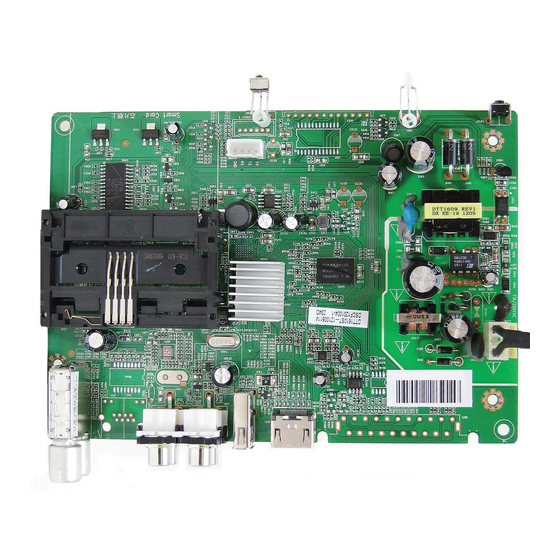
2.2 COMPONENT LAYOUT OF POWER SUPPLY 3 SCHEMATIC.COMPONENT LAYOUT AND BOM OF MAIN BOARD 3.1 SCHEMATIC OF MAIN BOARD... - Page 22 HISTORY OF MODIFICATIONS REV. CHECK.BY APP.BY DATE Version History BLOCK DIAGRAM V1.0: 2011-07-24 Created LOW IF T2 DEMOD TUNER I2C,AGC (MSB1230) CVBS Y/PB/PR Video buffer DDR3 (128MB) SCART Audio OP Serial FLASH (4MB) MSD5043-V60 SPDIF Nand FLASH HDMI1.3 (128MB) EEPROM (2KB) RJ45 POWER...
- Page 23 HISTORY OF MODIFICATIONS REV. CHECK.BY APP.BY DATE GPIO MAPPING: MODE_0 USAGE USAGE DETAIL NOTE PM_GPIO0 /FLASH_WP SFLASH PM_GPIO1 RGB/CVBS SCART PM_GPIO2 16:9/4:3 SCART PM_GPIO3 TV/AV SCART PD_CTRL PD_CTRL POWER CTRL PM_GPIO5 ANT_PWR_CTRL TUNER PM_GPIO6 ANT_OVERLOAD TUNER MUTE_CTRL AUDIO_MUTE PM_GPIO8 S_GPIO1 USB_OCD S_GPIO2 /USB_CTRL...
- Page 24 HISTORY OF MODIFICATIONS REV. CHECK.BY APP.BY DATE U401-A HW STRAP close MStar IC MSD5043-V60 VCC3_3V_PD RF_AGC HDMI_CEC HDMI_HPD R430 IF_AGC HSYNC_/_HDMI_HDP IM_Q DEMOD HDMI_CH2_P HDMI-TX2P R431 CI_OEZ IP_Q HDMI_CH2_M HDMI-TX2N CHIP_CONFIG[3] IM_I HDMI_CH1_P HDMI-TX1P R432 HDMI IP_I HDMI_CH1_M HDMI-TX1N R433 CI_WEZ HDMI_CH0_P HDMI-TX0P...
- Page 25 HISTORY OF MODIFICATIONS REV. CHECK.BY APP.BY DATE VDDC1V2 VDDC1V2 VDDC_1V2 M12 VDDC_1V2 N11 40mil VDDC_1V2 N12 VDDC_1V2 P11 VDDC_1V2 P12 C454 C455 C447 C448 C449 C450 C451 C452 C453 VDDC_1V2 R11 10uF 10uF VDDC_1V2 R12 0805 0805 VDDC_1V2 M10 AVDD12_HDMI DVDD12_DDR VCC3_3V_PD AVDD_DDR_DATA...
- Page 26 HISTORY OF MODIFICATIONS REV. CHECK.BY APP.BY DATE Serial NOR FLASH U403 1V5D M25PX64 F_NCA2 NC E2 F_NCE1 R459 F_NCA3 NC E3 F_NCE2 B_MADR13 B-MADR13 R460 F_NCA4 NC E4 F_NCE3 B_MADR9 B-MADR9 NC E5 F_NCE4 R461 B_BA0 M1-BA0 F_NCB1 R462 M1_BA2 M1-BA2 SPI_CLK [3,5]...
- Page 27 HISTORY OF MODIFICATIONS REV. CHECK.BY APP.BY DATE HDMI J601 TX2+ TX2SD R601 HDMI-TX2P R602 TX2- HDMI-TX2N USB Power R603 TX1+ HDMI-TX1P R604 HDMI-TX1N TX1SD TX1- 5V_USB R605 HDMI-TX0P TX0+ J501 R606 HDMI-TX0N TX0SD R607 R501 HDMI-TXCLKP USB1_DM R608 R502 TX0- HDMI-TXCLKN USB1_DP HD5V...
- Page 28 HISTORY OF MODIFICATIONS REV. CHECK.BY APP.BY DATE AUDIO OP 4:3/16:9 Control AV/TV 16:9/4:3 GPIO MODE (GPIOxx) (GPIOxx) R223 390K 16:9 (5V~8V) J801 C222 6.8P R225 330R (9.5V~12V) LINE_OUT_L LINE_OUT_R R/OUT (0V) 5VA_A C226 R227 UVP>1.15V 0.33uF R/IN R233 R234 LINE_OUT_L L/OUT 5VA_A R215...
- Page 29 HISTORY OF MODIFICATIONS REV. CHECK.BY APP.BY DATE Half NIM Tuner TUNER2 VA4M1EX2124 ANTENNA_POWER AVDD1.8V AVDD3V ANT_POWER B1(1.8V) B2(3.3V) R744 100R SDA_T R745 100R SCL_T XOUT VCC3_3V_PD AVDD3V C744 C745 IF_AGC L751 22uH IF1+ 0805 IF1- C752 CE751 470uf/10v IFAGC IP_Q IM_Q ANTENNA_POWER VCC5V_PD...
- Page 30 HISTORY OF MODIFICATIONS REV. CHECK.BY APP.BY DATE R676 300K EDVDD3_3V EDVDD3_3V EDVDD3_3V EAVDD3_3V VDDCR EDVDD3_3V R677 ETH_RST C663 R674 R675 1.5K R665 100R R678 ET_MDIO MDIO MDIOTX+ R679 R666 100R MDIOTX- ET_MDC R680 RXP 22 MDIORX+ R681 RXER/PHYAD0 RXER/PHYAD0 MDIORX- QFN24P ET_TXEN TXEN...
- Page 31 HISTORY OF MODIFICATIONS REV. CHECK.BY APP.BY DATE DC/DC 3.3V 5V Switch VCC5V VCC5V_PD VCC5V VCC3_3V_PD Front Panel Connector U151 3.3V@600mA L181 NC/FB120R PAM2312/SY8008 L152 L151 0805 Q181 FB120R 4.7uH/1A 0805 C152 C153 L121 101T R152 C155 C151 CE152 VCC5V 10uF DMP2225L 0805 10uF...
- Page 32 HISTORY OF MODIFICATIONS REV. CHECK.BY APP.BY DATE AC-DC RT901 10D-9 D912 D913 T901 C921 R928 CN902 LF902 IN4007 IN4007 22R 0805 102 0805 C913 R921 R922 472/1KV 200K 1206 200K 1206 L902 D911 D910 D917 1N5822 C910 C911 VCC5V 4.7uH/2A 3PIN 3.96MM 10uF/400V 22uf/400v...
- Page 37 深圳九洲公司 ShenzhenJiuzhouCo.,LtDR. BOMNo. DTT1609 Version Released 制作人名 Item Q'ty Location Remark L302 L303 L304 L305 L306 贴片磁珠GZ1005D601TF,600 ohm,200MA,1005 L171 L201 L251 L252 L301 L401 L462 L463 L464 L481 L561 L702 BG1608B101BF 100 ohm 100M 0603 L704 L705 L706 L707 L708 L710 L131 L141 L151 L703 L751 CBG201209U101T/BG2012B101TF, 100 ohm 300MA L142 L152...
- Page 38 C217 C219 C-CERAMIC, CHIP ; 2.2uF, +80-20%, 16V, Y5V, TP,2012 C135 C143 C153 C-CERAMIC, CHIP ;10UF, 10%, 6.3V, X5R, TP,2012, C107 C112 C115 C131 C141 C151 C415 C426 C454 C455 C456 C-CERAMIC, CHIP ; 10uF, +80-20%, 10V, Y5V, TP,2012 C463 C472 C474 C482 C501 C753 R171 R215 R217 R401 R405 R446 R447 R448 R449 R457 R458 R459 R460 R461 R462 R463 R464 R465 R466 R467 R468 R469 R470 R471 R472 R473 R474 R475 R476 R477 R478 R479 R480...
- Page 39 R142 R-CHIP ; 150K ohm, 1%, 1/16W, DA, TP, 1005 R529 R568 R-CHIP; 0 Ohm 5%, 1/10W, DA, TP, 1608 R920 R-CHIP; 470 Ohm 5%, 1/10W, DA, TP, 1608 R923 R925 R-CHIP , 1Kohm, 5%, 1/10W, DA, TP, 1608 R594 R595 R918 R-CHIP;...
- Page 40 U701 Digital DVB-T/T2 Demodulator:MSB1230 - LF,64-pin LQFP U201 Capless 2Vrms to 3Vrms Line Driver with Adjustable Gain:SGM8905 MSOP-10 U401 DVB-T/C HD STB System-on-Chip:MSD5043-I00,BGA-417 J601 HDMI 座: 51U019S-301N-A-B*//161A0012 ,19PIN,Pitch=0.5mm DTT1609MB 2011-12-20 167.5*(117.5*2)MM (双面板) Item Q'ty Location Remark L902 IND-MOLDED,4.7UH Ferrite DR2W6*8.3-4.7UH/4.7uH DR2W6*8 L132 IND-MOLDED,22uH Ferrite 3A DR2W9*12-220K-PVC/22uh DR2W9*12 CE171 CE172 CE402...
- Page 41 FOR D191 LED SUPPORT 12MM J501 USB-A-04,USB插座,侧弯90度 SW101 SWITCH PUSH 6X6X2DH5 H:1.5mm TUNER2 DVB-T2/T TUNER:FH-RT232A4 9+2PINS 立式 (FOR U401) Heat SINK(25*25*20 white )
- Page 42 # OTHER TROUBLESOOTHING 1, Testing the chip and the DEMOD's crystal frequency(Y401 Y701) with a frequency spectrograph, to make sure it's within ±20PPM(±480HZ); 2, If there is a heavy mosaic when your STB works, or even NO SIGNAL, please change the crystal in the TUNER;...
- Page 43 3, If the fuse blew out, please change the F902 and check the D910,D911,D912,D913,to see if they are burnout.
Need help?
Do you have a question about the SRT8500 and is the answer not in the manual?
Questions and answers