Table of Contents
Advertisement
Quick Links
Advertisement
Table of Contents

Related Manuals for Cypress CY7C68013


Summary of Contents for Cypress CY7C68013
- Page 1 68013 CY7C68013 CY7C68013 ® ™ EZ-USB USB Microcontroller High-Speed USB Peripheral Controller Cypress Semiconductor Corporation • 3901 North First Street • San Jose • CA 95134 • 408-943-2600 Document #: 38-08012 Rev. *A Revised January 15, 2002...
-
Page 2: Table Of Contents
3.15 Autopointer Access ........................17 3.16 I C-compatible Controller ......................17 4.0 PIN ASSIGNMENTS ........................18 4.1 CY7C68013 Pin Descriptions ...................... 23 5.0 REGISTER SUMMARY ........................30 6.0 ABSOLUTE MAXIMUM RATINGS ....................36 7.0 OPERATING CONDITIONS ......................36 8.0 DC CHARACTERISTICS ....................... 36 9.0 AC ELECTRICAL CHARACTERISTICS .................. - Page 3 Figure 4-2. CY7C68013 128-pin TQFP Pin Assignment..............19 Figure 4-3. CY7C68013 100-pin TQFP Pin Assignment..............20 Figure 4-4. CY7C68013 56-pin SSOP Pin Assignment ..............21 Figure 9-1. Program Memory Read Timing Diagram ................ 36 Figure 9-2. Data Memory Read Timing Diagram ................37 Figure 9-3.
- Page 4 CY7C68013 LIST OF TABLES Table 3-1. Default ID Values for FX2 ....................8 Table 3-2. INT2 USB Interrupts ......................9 Table 3-3. Individual FIFO/GPIF Interrupt Sources ................10 [1, 2] Table 3-4. Default Full-Speed Alternate Settings ................ 14 [1, 2] Table 3-5.
-
Page 5: Ez-Usb® Fx2™ Features
USB 2.0 integrated microcontroller. By integrating the USB 2.0 transceiver, SIE, enhanced 8051 microcontroller, and a programmable peripheral interface in a single chip, Cypress has created a very cost- effective solution that provides superior time-to-market advantages. The ingenious architecture of FX2 results in data transfer rates of 56 Mbytes per second, the maximum allowable USB 2.0 bandwidth, while still using a low-cost 8051 microcontroller in... -
Page 6: Applications
• MP3 players • Networking. The “Reference Designs” section of the cypress website provides additional tools for typical USB 2.0 applications. Each reference design comes complete with firmware source and object code, schematics, and documentation. Please visit http://www.cypress.com/usb for more information. -
Page 7: I 2 C-Compatible Bus
CY7C68013 3.2.1 8051 Clock Frequency FX2 has an on-chip oscillator circuit that uses an external 24-MHz (±100 ppm) crystal with the following characteristics: • Parallel resonant • Fundamental mode • 500 µW drive level • 27–33 pF (5% tolerance) load capacitors. -
Page 8: Usb Boot Methods
CY7C68013 SCON1 EXIF INT2CLR SBUF1 DPL0 MPAGE INT4CLR DPH0 DPL1 DPH1 PCON TCON SCON0 T2CON EICON TMOD SBUF0 AUTOPTRH1 EP2468STAT EP01STAT RCAP2L AUTOPTRL1 EP24FIFOFLGS GPIFTRIG RCAP2H reserved EP68FIFOFLGS AUTOPTRH2 GPIFSGLDATH CKCON AUTOPTRL2 GPIFSGLDATLX reserved AUTOPTRSETUP GPIFSGLDATLNOX USB Boot Methods During the power-up sequence, internal logic checks the I C-compatible port for the connection of an EEPROM whose first byte is either 0xC0 or 0xC2. -
Page 9: Table 3-2. Int2 Usb Interrupts
CY7C68013 3.7.2 USB-Interrupt Autovectors The main USB interrupt is shared by 27 interrupt sources. To save the code and processing time that normally would be required to identify the individual USB interrupt source, the FX2 provides a second level of interrupt vectoring, called Autovectoring. When a USB interrupt is asserted, the FX2 pushes the program counter onto its stack then jumps to address 0x0043, where it expects to find a “jump”... -
Page 10: Reset And Wakeup
CY7C68013 3.7.3 FIFO/GPIF Interrupt (INT4) Just as the USB Interrupt is shared among 27 individual USB-interrupt sources, the FIFO/GPIF interrupt is shared among 14 individual FIFO/GPIF sources. The FIFO/GPIF Interrupt, like the USB Interrupt, can employ autovectoring. Table 3-3 shows the priority and INT4VEC values for the 14 FIFO/GPIF interrupt sources Table 3-3. -
Page 11: Figure 3-1. Internal Code Memory, Ea = 0
CY7C68013 3.9.2 Internal Code Memory, EA = 0 This mode implements the internal eight-kbyte block of RAM (starting at 0) as combined code and data memory. When external RAM or ROM is added, the external read and write strobes are suppressed for memory spaces that exist inside the chip. This allows the user to connect a 64-kbyte memory without requiring address decodes to keep clear of internal memory spaces. -
Page 12: Figure 3-2. External Code Memory, Ea = 1
CY7C68013 3.9.3 External Code Memory, EA = 1 The bottom eight kbytes of program memory is external, and therefore the bottom eight kbytes of internal RAM is accessible only as data memory. Inside FX2 Outside FX2 FFFF 7.5 kbytes (OK to populate... -
Page 13: Register Addresses
CY7C68013 3.10 Register Addresses FFFF 4 kbytes EP2-EP8 buffers (8 × 512) F000 EFFF 2 kbytes RESERVED E800 E7FF 64 bytes EP1IN E7C0 E7BF 64 bytes EP1OUT E780 E77F 64 bytes EP0 IN/OUT E740 E73F 64 bytes RESERVED E700 E6FF... -
Page 14: Figure 3-3. Endpoint Configuration
CY7C68013 3.11.4 Endpoint Configurations (High-speed Mode) EP0 IN&OUT EP1 IN EP1 OUT 1024 1024 1024 1024 1024 1024 1024 1024 1024 1024 1024 Figure 3-3. Endpoint Configuration Endpoints 0 and 1 are the same for every configuration. Endpoint 0 is the only CONTROL endpoint, and endpoint 1 can be either BULK or INTERRUPT. -
Page 15: External Fifo Interface
GPIF The GPIF is a flexible 8- or 16-bit parallel interface driven by a user-programmable finite state machine. It allows the CY7C68013 to perform local bus mastering, and can implement a wide variety of protocols such as ATA interface, printer parallel port, and Utopia. -
Page 16: Usb Uploads And Downloads
(or multiple inputs) must be before proceeding. The GPIF vector can be programmed to advance a FIFO to the next data value, advance an address, etc. A sequence of the GPIF vectors make up a single waveform that will be executed to perform the desired data move between the CY7C68013 and the external design. 3.13.1 Six Control OUT Signals The 100- and 128-pin packages bring out all six Control Output pins (CTL0-CTL5). -
Page 17: Pin Assignments
CY7C68013 Table 3-6. Strap Boot EEPROM Address Lines to These Values Bytes Example EEPROM 24LC00 24LC01 24LC02 24LC32 24LC64 3.16.2 C-compatible Interface Boot Load Access At power-on reset the I C-compatible interface boot loader will load the VID/PID/DID/a configuration byte and up to 8 kbytes of program/data. -
Page 18: Figure 4-1. Signals
CY7C68013 Port GPIF Master Slave FIFO FD[15] FD[15] FD[14] FD[14] FD[13] FD[13] FD[12] FD[12] FD[11] FD[11] FD[10] FD[10] FD[9] FD[9] FD[8] FD[8] FD[7] FD[7] FD[6] FD[6] FD[5] FD[5] FD[4] FD[4] FD[3] FD[3] FD[2] FD[2] FD[1] FD[1] FD[0] FD[0] XTALIN SLRD... -
Page 19: Figure 4-2. Cy7C68013 128-Pin Tqfp Pin Assignment
PA2/*SLOE PA1/INT1# PA0/INT0# PC7/GPIFADR7 PC6/GPIFADR6 PC5/GPIFADR5 PC4/GPIFADR4 INT4 PC3/GPIFADR3 PC2/GPIFADR2 PC1/GPIFADR1 PC0/GPIFADR0 IFCLK CTL2/*FLAGC RESERVED CTL1/*FLAGB BKPT CTL0/*FLAGA CTL4 CTL3 Figure 4-2. CY7C68013 128-pin TQFP Pin Assignment * denotes programmable polarity Document #: 38-08012 Rev. *A Page 19 of 48... -
Page 20: Figure 4-3. Cy7C68013 100-Pin Tqfp Pin Assignment
100-pin TQFP DPLUS PC7/GPIFADR7 DMINUS PC6/GPIFADR6 PC5/GPIFADR5 PC4/GPIFADR4 PC3/GPIFADR3 INT4 PC2/GPIFADR2 PC1/GPIFADR1 PC0/GPIFADR0 CTL2/*FLAGC IFCLK CTL1/*FLAGB RESERVED CTL0/*FLAGA BKPT CTL4 CTL3 Figure 4-3. CY7C68013 100-pin TQFP Pin Assignment * denotes programmable polarity Document #: 38-08012 Rev. *A Page 20 of 48... -
Page 21: Figure 4-4. Cy7C68013 56-Pin Ssop Pin Assignment
PA4/FIFOADR0 PA3/*WU2 DPLUS PA2/*SLOE DMINUS PA1/INT1# PA0/INT0# CTL2/*FLAGC IFCLK CTL1/*FLAGB RESERVED CTL0/*FLAGA PB0/FD0 PB7/FD7 PB1/FD1 PB6/FD6 PB2/FD2 PB5/FD5 PB3/FD3 PB4/FD4 Figure 4-4. CY7C68013 56-pin SSOP Pin Assignment * denotes programmable polarity Document #: 38-08012 Rev. *A Page 21 of 48... -
Page 22: Cy7C68013 Pin Descriptions
CY7C68013 CY7C68013 Pin Descriptions Table 4-1. FX2 Pin Descriptions Name Type Default Description AVCC Power Analog V . This signal provides power to the analog section of the chip. AGND Power Analog Ground. Connect to ground with as short a path as possible. - Page 23 CY7C68013 Table 4-1. FX2 Pin Descriptions (continued) Name Type Default Description Input External Access. This pin determines where the 8051 fetches code between addresses 0x0000 and 0x1FFF. If EA = 0 the 8051 fetches this code from its internal RAM. IF EA = 1 the 8051 fetches this code from external memory.
- Page 24 CY7C68013 Table 4-1. FX2 Pin Descriptions (continued) Name Type Default Description PA7 or I/O/Z Multiplexed pin whose function is selected by the IFCONFIG[1:0] and FLAGD or (PA7) PORTACFG.7 bits. SLCS# PA7 is a bidirectional I/O port pin. FLAGD is a programmable slave-FIFO output status flag signal.
- Page 25 CY7C68013 Table 4-1. FX2 Pin Descriptions (continued) Name Type Default Description PC5 or I/O/Z Multiplexed pin whose function is selected by PORTCCFG.5 GPIFADR5 (PC5) PC5 is a bidirectional I/O port pin. GPIFADR5 is a GPIF address output pin. PC6 or I/O/Z Multiplexed pin whose function is selected by PORTCCFG.6...
- Page 26 CY7C68013 Table 4-1. FX2 Pin Descriptions (continued) Name Type Default Description PE3 or I/O/Z Multiplexed pin whose function is selected by the PORTECFG.3 bit. RXD0OUT (PE3) PE3 is a bidirectional I/O port pin. RXD0OUT is an active-HIGH signal from 8051 UART0. If RXD0OUT is selected and UART0 is in Mode 0, this pin provides the output data for UART0 only when it is in sync mode.
- Page 27 CY7C68013 Table 4-1. FX2 Pin Descriptions (continued) Name Type Default Description CTL3 Output CTL3 is a GPIF control output. CTL4 Output CTL4 is a GPIF control output. CTL5 Output CTL5 is a GPIF control output. IFCLK I/O/Z Interface Clock, used for synchronously clocking data into or out of the slave FIFOs.
- Page 28 CY7C68013 Table 4-1. FX2 Pin Descriptions (continued) Name Type Default Description Power . Connect to 3.3V power source. Power . Connect to 3.3V power source. Power . Connect to 3.3V power source. Power . Connect to 3.3V power source. Power .
-
Page 29: Register Summary
CY7C68013 Register Summary FX2 register bit definitions are described in the FX2 TRM in greater detail. Table 5-1. FX2 Register Summary Hex Size Name Description Default Access GPIF Waveform Memories E400 128 WAVEDATA GPIF Waveform Descriptor xxxxxxxx 0, 1, 2, 3 data... - Page 30 CY7C68013 Table 5-1. FX2 Register Summary (continued) Hex Size Name Description Default Access [ 6 ] E631 EP2FIFOPFL Endpoint 2 / slave FIFO Pro- IN:PKTS[1] IN:PKTS[0] PFC5 PFC4 PFC3 PFC2 PFC1 PFC0 00000000 grammable Flag L OUT:PFC7 OUT:PFC6 [ 6 ]...
- Page 31 CY7C68013 Table 5-1. FX2 Register Summary (continued) Hex Size Name Description Default Access E669 reserved INPUT / OUTPUT E670 PORTACFG I/O PORTA Alternate Config- FLAGD SLCS INT1 INT0 00000000 uration E671 PORTCCFG I/O PORTC Alternate Con- GPIFA7 GPIFA6 GPIFA5 GPIFA4...
- Page 32 CY7C68013 Table 5-1. FX2 Register Summary (continued) Hex Size Name Description Default Access EP2FIFOBCL Endpoint 2 slave FIFO total 00000000 byte count L EP4FIFOBCH Endpoint 4 slave FIFO total BC10 00000000 byte count H E6AE EP4FIFOBCL Endpoint 4 slave FIFO total...
- Page 33 CY7C68013 Table 5-1. FX2 Register Summary (continued) Hex Size Name Description Default Access reserved reserved E6E2 EP6GPIFFLGSEL Endpoint 6 GPIF Flag select 00000000 [ 6 ] E6E3 EP6GPIFPFSTOP Endpoint 6 GPIF stop trans- FIFO6FLAG 00000000 action on prog. flag [ 6 ]...
- Page 34 CY7C68013 Table 5-1. FX2 Register Summary (continued) Hex Size Name Description Default Access [ 7 ] AUTOPTRH1 Autopointer 1 Address H 00000000 [ 7 ] AUTOPTRL1 Autopointer 1 Address L 00000000 reserved [ 7 ] AUTOPTRH2 Autopointer 2 Address H...
-
Page 35: Absolute Maximum Ratings
CY7C68013 Absolute Maximum Ratings Storage Temperature ............................ –65°C to +150°C Ambient Temperature with Power Supplied ......................0°C to +70°C Supply Voltage to Ground Potential ........................–0.5V to +4.0V DC Input Voltage to Any Input Pin ..........................5.25V DC Voltage Applied to Outputs in High Z State ..................–0.5V to V + 0.5V... -
Page 36: Ac Electrical Characteristics
CY7C68013 AC Electrical Characteristics USB Transceiver USB 2.0-compliant in full- and high-speed modes. Program Memory Read CLKOUT A[15..0] STBH STBL PSEN# [10] ACC1 D[7..0] data in SOEL SCSL Figure 9-1. Program Memory Read Timing Diagram Table 9-1. Program Memory Read Parameters... -
Page 37: Data Memory Read
CY7C68013 Data Memory Read Stretch = 0 CLKOUT A[15..0] STBH STBL SCSL SOEL [11] ACC1 D[7..0] data in Stretch = 1 CLKOUT A[15..0] [11] ACC1 D[7..0] data in Figure 9-2. Data Memory Read Timing Diagram Note: 11. t and t... -
Page 38: Data Memory Write
CY7C68013 Data Memory Write CLKOUT STBL STBH A[15..0] SCSL OFF1 data out D[7..0] Stretch = 1 CLKOUT A[15..0] OFF1 D[7..0] data out Figure 9-3. Data Memory Write Timing Diagram Table 9-3. Data Memory Write Parameters Parameter Description Min. Max. Unit... -
Page 39: Gpif Synchronous Signals
CY7C68013 GPIF Synchronous Signals IFCLK IFCLK GPIFADR[8:0] DATA(input) valid XCTL DATA(output) [12] Figure 9-4. GPIF Synchronous Signals Timing Diagram [13, 14] Table 9-4. GPIF Synchronous Signals Parameters with Internally Sourced IFCLK Parameter Description Min. Max. Unit IFCLK Period 20.83 IFCLK... -
Page 40: Slave Fifo Synchronous Read
CY7C68013 Slave FIFO Synchronous Read IFCLK IFCLK SLRD XFLG FLAGS DATA OEon OEoff SLOE [12] Figure 9-5. Slave FIFO Synchronous Read Timing Diagram [14] Table 9-6. Slave FIFO Synchronous Read Parameters with Internally Sourced IFCLK Parameter Description Min. Max. Unit IFCLK Period 20.83... -
Page 41: Slave Fifo Asynchronous Read
CY7C68013 Slave FIFO Asynchronous Read RDpwh SLRD RDpwl XFLG FLAGS DATA OEon OEoff SLOE [12] Figure 9-6. Slave FIFO Asynchronous Read Timing Diagram [15] Table 9-8. Slave FIFO Asynchronous Read Parameters Parameter Description Min. Max. Unit SLRD Pulse Width LOW... -
Page 42: Slave Fifo Asynchronous Write
CY7C68013 [14] Table 9-10. Slave FIFO Synchronous Write Parameters with Externally Sourced IFCLK Parameter Description Min. Max. Unit IFCLK Period 20.83 IFCLK SLWR to Clock Set-up Time 12.1 Clock to SLWR Hold Time FIFO Data to Clock Set-up Time Clock to FIFO Data Hold Time Clock to FLAGS Output Propagation Time 13.5... -
Page 43: Slave Fifo Asynchronous Packet End Strobe
CY7C68013 [14] Table 9-13. Slave FIFO Synchronous Packet End Strobe Parameters with Externally Sourced IFCLK Parameter Description Min. Max. Unit IFCLK Period 20.83 IFCLK PKTEND to Clock Set-up Time Clock to PKTEND Hold Time Clock to FLAGS Output Propagation Delay 13.5... -
Page 44: Slave Fifo Synchronous Address
CY7C68013 Table 9-16. Slave FIFO Address to Flags/Data Parameters Parameter Description Min. Max. Unit FIFOADR[1:0] to FLAGS Output Propagation Delay 10.7 XFLG FIFOADR[1:0] to FIFODATA Output Propagation Delay 14.3 9.14 Slave FIFO Synchronous Address IFCLK SLCS/FIFOADR [1:0] Figure 9-13. Slave FIFO Synchronous Address Timing Diagram [14] Table 9-17. -
Page 45: Package Diagrams
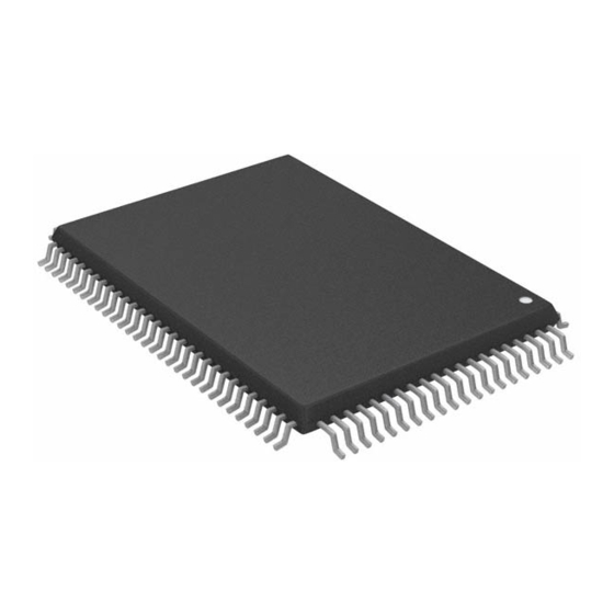
CY7C68013 11.0 Package Diagrams The FX2 is available in three packages: • 56-pin SSOP • 100-pin TQFP • 128-pin TQFP. 51-85062-C Figure 11-1. 56-lead Shrunk Small Outline Package O56 Document #: 38-08012 Rev. *A Page 45 of 48... -
Page 46: Figure 11-2. 100-Pin Thin Plastic Quad Flatpack (14 X 20 X 1.4 Mm) A101
CY7C68013 51-85050-A Figure 11-2. 100-Pin Thin Plastic Quad Flatpack (14 x 20 x 1.4 mm) A101 Document #: 38-08012 Rev. *A Page 46 of 48... -
Page 47: Figure 11-3. 128-Lead Thin Plastic Quad Flatpack (14 X 20 X 1.4 Mm) A128
Cypress Semiconductor product. Nor does it convey or imply any license under patent or other rights. Cypress Semiconductor does not authorize its products for use as critical components in life-support systems where a malfunction or failure may reasonably be expected to result in significant injury to the user. The inclusion of Cypress... - Page 48 CY7C68013 Document Title: CY7C68013 EZ USB FX2 USB Microcontroller, High Speed USB Peripheral Controller Document Number: 38-08012 Issue Orig. of REV. ECN NO. Date Change Description of Change 111753 11/15/01 Change from Spec number: 38-00929 to 38-08012 111802 02/20/02 Update functional changes between revision D part and revision E part Changed timing data from simulation data to revision E characterization data Document #: 38-08012 Rev.
Need help?
Do you have a question about the CY7C68013 and is the answer not in the manual?
Questions and answers