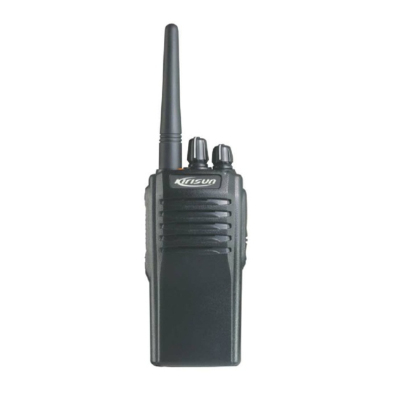
Kirisun PT4208 Service Manual
Professional fm handheld transceiver
Hide thumbs
Also See for PT4208:
- Service manual (53 pages) ,
- Instruction manual (22 pages) ,
- Instruction manual (22 pages)
Table of Contents
Advertisement
Quick Links
Dangerous!
Do not connect the AC power or DC power over
8.6V with any connector or terminal of the radio.
Otherwise it will cause fire, electric shock or
damage to the radio.
Warning!
Do not reverse power connection.
It may cause harm to the radio if signal input on
the antenna connector is bigger than 20 dBm
(100mW).
Do not turn on the power before the antenna or
load connection is completed.
If the antenna has been damaged, do not use the
radio. Damaged antenna may cause lightly burning
on skin.
Though the radio is waterproof, it's better to
avoid putting it in rain or snow, or any other liquid
to ensure its life and performance.
Statement!
Kirisun Electronics (Shenzhen) Co., Ltd owns
the copyright of KSP4208 software.
Unauthorized Duplication of KSP4208 software
is strictly prohibited.
Kirisun Electronics (Shenzhen) Co., Ltd owns
the copyright of the MCU software.
Kirisun Electronics (Shenzhen) Co., Ltd owns
the copyright of the radio outward/structure/circuit
design.
Kirisun Electronics (Shenzhen) Co., Ltd owns
the copyright of this service manual. Unauthorized
publication is prohibited.
Kirisun Electronics (Shenzhen) Co., Ltd owns
the trademarks "KIRISUN", "
Chapter 1 Overview..............................................................................1
Chapter 2 Radio Overview.......................................................................1
Chapter 3 Circuit Introduction...................................................................2
Chapter 4 Mode Introduction....................................................................8
Chapter 5 Maintenance, Assembly and Disassembly.......................................10
Chapter 6 Overall Debugging..................................................................12
Chapter 7 Major Specifications................................................................15
Chapter 8 Trouble Shootings and Solutions .................................................15
Chapter 9 KBC-70C Charger..................................................................16
Appendix 1 Abbreviations......................................................................17
Appendix 2 Electronic components list.......................................................18
Appendix 3 Damageable components list.....................................................23
Appendix 4 Framework components list......................................................25
Appendix 5 Accessories.........................................................................26
Figure 1 PT4208 Schematic Circuit Diagram (420-470MHz).............................27
Figure 2 PT4208 Main Board Schematic Circuit Diagram (420-470MHz)..............28
Figure 3 PT4208 Top Main Board Position Mark Diagram (420-470MHz).............29
Figure 4 PT4208 Bottom Main Board Position Mark Diagram (420-470MHz).........30
Figure 5 PT4208 Top Main Board Numerical Value Diagram (420-470MHz)..........31
Figure 6 PT4208 Bottom Main Board Numerical Value Diagram (420-470MHz)......32
Figure 7 PT4208 Top Main Board Circuit Connection Diagram (420-470MHz).......33
Figure 8 PT4208 Bottom Main Board Circuit Connection Diagram (420-470MHz)...34
Figure 9 PT4208 Main Board Schematic Circuit Diagram (136-174MHz)..............35
Figure 10 PT4208 Top Main Board Position Mark Diagram (136-174MHz)............36
Figure 11 PT4208 Bottom Main Board Position Mark Diagram (136-174MHz).......37
Figure 12 PT4208 Top Main Board Numerical Value Diagram (136-174MHz).........38
Figure 13 PT4208 Bottom Main Board Numerical Value Diagram (136-174MHz)....39
Figure 14 PT4208 Top Main Board Circuit Connection Diagram (136-174MHz)......40
Figure 15 PT4208 Bottom Main Board Circuit Connection Diagram (136-174MHz).41
Figure 16 KBC-70C Schematic Circuit Diagram............................................42
Figure 17 KBC-70C Top Main Board Numerical Value Diagram.........................43
Figure 18 KBC-70C Top Main Board Position Mark Diagram............................44
Figure 19 KBC-70C Bottom Main Board Numerical Value Diagram.....................45
Figure 20 KBC-70C Bottom Main Board Position Mark Diagram........................46
Figure 21 KBC-70C Circuit Connection Diagram..........................................47
", "科立讯".
PT4208 Service Manual
Contents
Advertisement
Table of Contents

Related Manuals for Kirisun PT4208


Summary of Contents for Kirisun PT4208
-
Page 1: Table Of Contents
Damaged antenna may cause lightly burning Figure 2 PT4208 Main Board Schematic Circuit Diagram (420-470MHz)…………..28 on skin. Figure 3 PT4208 Top Main Board Position Mark Diagram (420-470MHz)………….29 Though the radio is waterproof, it's better to Figure 4 PT4208 Bottom Main Board Position Mark Diagram (420-470MHz)……...30 avoid putting it in rain or snow, or any other liquid Figure 5 PT4208 Top Main Board Numerical Value Diagram (420-470MHz)……….31... -
Page 2: Chapter 1 Overview
PT4208-02 Triode 2SC5108(Y) 104-SC5108-001 PT4208 portable radios, and is for the engineers and qualified technicians that have been trained by our company. 1.3 Service In this manual you can find all the information of product All the Kirisun products are subject to the service service. -
Page 3: Chapter 3 Circuit Introduction
PT4208 Service Manual Channel Selector Knob Front End of Receiver Rotate the knob to select channels 1-16. Signals from the antenna are filtered by BPF which Power/Volume Control Knob consists of C37, C227, L8, L15, C70, C126, D30, C218, L9,... - Page 4 PT4208 Service Manual drive the speaker after collecting the receiving audio signals, voice prompt signals, alert tone signals and warning tone signals. The warning tone has no volume limitation. When AFCO is in high level, Q35 is on, IC8 begins to work and the speaker sounds.
- Page 5 Figure 3.8 Schematic Diagram for Frequency Synthesizer Prompt” key. The speaker will voice the current channel number under The PT4208 adopts PLL frequency synthesizer. standby state if the Voice Prompt Function is set and the Frequency synthesizer consists of reference oscillator, “Voice Prompt”...
- Page 6 MCU controls the operation of every unit to realize all The radio has 39 groups of standard CTCSS frequency functions of the PT4208. for your selection, refer to Table 3.1. Communication with external PC...
- Page 7 PT4208 Service Manual The distribution of each pin goes as table 3.3. 74.4 103.5 146.2 210.7 Table 3.3 Definition of CPU Base Pin: 77.0 107.2 151.4 218.1 No. Port name Pin Name Function 79.7 110.9 156.7 225.7 1 TOPKEY Programmable Top Key Detection 82.5...
- Page 8 PT4208 Service Manual DTC144EE 5C Switch RSSI I(A/D7) Signal Strength Detection BUSY I(A/D6) Busy Signal Input KTA1298 5T Switch MANDO I(A/D5) Rewind Switch Detection KTA1298 Voltage Regulation Output Current Stretching BATT I(A/D4) Battery Voltage Detection KTA1298 5R Switch Connect Pull-down Resistor with VSS...
-
Page 9: Chapter 4 Mode Introduction
PT4208 Service Manual Install KSP4208 on the computer. Table 3.8 Schematic diagram for semiconductor devices As shown in the figure below, connect the radio to the packaging serial port of the computer with the special programming cable (KSPL-09). 2SC5108 2SC3356... - Page 10 PT4208 Service Manual frequency. (stepping frequency: 2.5KHz / 5KHz / (4) Level-9 broadband of squelch level opens five frequency 6.25KHz) points Channel receiving signaling transmitting (5) Level-9 broadband of squelch level closes five frequency signaling points None (6) Level-9 narrowband of squelch level opens five CTCSS (60~260Hz @ 0.1Hz step)
-
Page 11: Chapter 5 Maintenance, Assembly And Disassembly
PT4208 Service Manual then click on “E.P” for downloading. Turn off the power to quit after the communication is successful. Just repeat steps 1-5 if you want to program another radio. Wired Clone Mode The radio will not exit automatically after entering wired clone mode if the wired clone function is set. - Page 12 PT4208 Service Manual properly; to remove the belt clip, insert your fingernail or a 2. Unsolder the antenna endpoint by electric iron, and then tool into the slot on the upper part of the belt clip and lift the remove the main board;...
-
Page 13: Chapter 6 Overall Debugging
PT4208 Service Manual Speaker/microphone Chapter 6 Overall Debugging 6.2 Debugging Items Some detection and adjustment shall be made to the 6.1 Equipment and software for debugging Equipment and software listed in table 6.1 are necessary radio’s technical data after changing the components during for maintenance and testing of the product. - Page 14 PT4208 Service Manual PT4208(3) 420.125MHz 445.125MHz 469.975MHz Double-click to enter “QT(670) frequency offset” in 6.3.2 PLL frequency calibration “Radio Performance Adjustment” Mode click Double-click to enter “6250HZ Frequency Stability”/ “Broadband” adjust five frequency points “2500HZ Frequency Stability” in “Radio Performance including ”Lowest”, “Low”, “Mid”, “High”...
- Page 15 PT4208 Service Manual “Radio Performance Adjustment” Mode, and adjust by the Adjustment” Mode for automatic detection of the software, same method except the open level of the RF signal changed and then click “Save” for exit after no or little variation in to 123dBm and the close level to 125dBm.
-
Page 16: Chapter 7 Major Specifications
PT4208 Service Manual CH : Transmitting Center Modulation Adjust Frequency Point ±200Hz Frequency Frequency ±4.5kHz AG:1kHz/220mV Offset deviator/Integrated Tester Check CH : Transmitting Center Modulation Frequency Frequency Point Sensitivity Offset AG:1kHz/22mV 2.2kHz~3.6kHz Frequency CTCSS Computer Adjust CTCSS:67Hz deviator/Integrated ±50Hz Test Mode ±0.75kHz... -
Page 17: Chapter 9 Kbc-70C Charger
PT4208 Service Manual charging turns to rapid charging. When the battery voltage No receiving A. The antenna is not in good contact. Please fasten signal the antenna head. reaches 9.6V±0.2V, the battery will be deemed as full and the B. The high-frequency amplifying tube Q20 is charging will be stopped. -
Page 18: Appendix 1 Abbreviations
PT4208 Service Manual Appendix 1 Abbreviations 9.5 LED Status Table: Charger status LED Status Charging Power Battery AMP: Amplify, amplifier Indicator LED (green) Temperature, ANT: Antenna (red) abnormality indicator APC: Automatic Power Control (yellow) BPF: Band Pass Filter Standby/battery CTCSS: Continuous Tone Control Squelch System... -
Page 19: Appendix 2 Electronic Components List
PT4208 Service Manual Appendix 2 Electronic components list No. Material Serial No. Component Name/Specification Unit Quantity 101-04208U-R04 PT4208PCB, FR-4, 1.2mm, PT4208U-081224, ROHS pcs 102-0R8C2A-R01 MCU / R8C/2A, R5F212A8SNFP, PLQP-64, ROHS IC10 102-9140NR-R01 Reset IC / PST9140NR, ROHS IC11 102-A31136-R01 IF(MF) modulation IC / TA31136FN, SSOP, ROHS... - Page 20 PT4208 Service Manual 108-450C24-R02 Chip phase frequency detector/ JTBM450CX24, ROHS 108-CF450G-R02 Chip porcelain filter/ LTWC450G, 450kHz±5kHz, ROHS 108-XF4995-R01 Chip IF filter / 49.95MHz±7.5KHz,U-5*2,ROHS pair XF1, XF2 109-040000-R01 Chip resistor / 0402,0R±5%,ROHS C67, C166, C250, R7, R24, R141, R182, R183, R217, R241, R260, R261, R278 109-040100-R01 Chip resistor / 0402,10R±5%,ROHS...
- Page 21 PT4208 Service Manual 104 109-040913-R01 Chip resistor / 0402,91K±5%,ROHS R213 105 109-060000-R01 Chip resistor / 0603,0R±5%,ROHS L16, L23, L34, L62, R23 106 109-060100-R01 Chip resistor / 0603,10R±5%,ROHS 107 109-060101-R01 Chip resistor / 0603,100R±5%,ROHS R74, R88 108 109-060154-R02 Chip resistor / 0603,150K±1%,ROHS...
- Page 22 PT4208 Service Manual 149 112-0435R0-R01 Chip capacitor / 0402,5P±0.25P,50V,C0G,ROHS C87, C118, C122, C145, C228 150 112-043681-R01 Chip capacitor / 0402,680P±10%,16V,X7R,ROHS C57, C258, C260 151 112-043683-R01 Chip capacitor / 0402, 0.068uF±10%, 16V, X7R, C242, C243, C247, C259 ROHS 152 112-043820-R01 Chip capacitor / 0402,82P±5%,50V,C0G,ROHS...
- Page 23 PT4208 Service Manual ROHS 193 114-06G181-R01 Chip inductor / LGHK1608R18J-T, 180nH±5%, 0603, L27, L50 ROHS 194 114-06G221-R02 Chip inductor / LGHK1608R22J-T, 220nH±5%, 0603, L49, L52 ROHS 195 114-06G270-R01 Chip inductor / MLG1608B27NJ, 27nH±5%, 0603, L12, L32, L33 ROHS 196 114-06G332-R01 Chip inductor / MLF1608A3R3K, 3.3uH±5%, 0603,...
-
Page 24: Appendix 3 Damageable Components List
PT4208 Service Manual Appendix 3:Damageable components list 17 18 23 24 25 26 32 33... - Page 25 PT4208 Service Manual Front Cabinet ASM. Part No. Description Part No. Description 201-004208-R01 Front Cabinet 204-003208-R02 Dust-proof Net for Speaker 201-004208-R09 Light guider 121-100000-R20 Speaker 201-004208-R08 Earphone cover 202-004208-R02 Rubber Key PTT 301-25080J-R01 Screw M2.5*8.0 201-004208-R04 Key PTT 204-004208-R02 Dust-proof Net for MIC...
-
Page 26: Appendix 4 Framework Components List
PT4208 Service Manual Appendix 4: Framework components list PART NUMBER DESCRIPTION NUMBER 121-100000-R20 SPEAKER 201-004208-R01A FRONT CABINET 201-004208-R02A COPING 201-004208-R03A SLIDE CROSSBAR 201-004208-R04A KEY PTT 201-004208-R05A POGO PIN SOCKET 201-004208-R06A VR KNOB 201-004208-R07A ENCODER KNOB 201-004208-R08A EARPHONE COVER 201-004208-R09A LIGHT GUIDER... -
Page 27: Appendix 5 Accessories
PT4208 Service Manual Appendix 5 Accessories Name Model Specification Accessories Battery KB-70B 7.4V 1700mAh Li-ion battery Hanging loop 8AJD-20K Earphone KME-014 KME-015 Charger KBC-70A 7 Hour Standard Charger DC OUT 12V 500mA Adaptor KTC-XX Antenna KA stubby antenna... - Page 28 PT4208 Service Manual Figure 1 PT4208 Schematic Circuit Diagram...
- Page 29 PT4208 Service Manual Figure 2 PT4208 Main Board Schematic Circuit Diagram (420-470MHz) 2T IN 150K...
- Page 30 PT4208 Service Manual Figure 3 PT4208 Top Main Board Position Mark Diagram (420-470MHz)
- Page 31 PT4208 Service Manual Figure 4 PT4208 Bottom Main Board Position Mark Diagram (420-470MHz)
- Page 32 PT4208 Service Manual Figure 5 PT4208 Top Main Board Numerical Value Diagram (420-470MHz)
- Page 33 PT4208 Service Manual Figure 6 PT4208 Bottom Main Board Numerical Value Diagram (420-470MHz)
- Page 34 PT4208 Service Manual igure 7 PT4208 Top Main Board Circuit Connection Diagram (420-470MHz)
- Page 35 PT4208 Service Manual Figure 8 PT4208 Bottom Main Board Circuit Connection Diagram (420-470MHz)
- Page 36 PT4208 Service Manual Figure 9 PT4208 Main Board Schematic Circuit Diagram (136-174MHz) 2T IN 33nH BLM11A221S...
- Page 37 PT4208 Service Manual Figure 10 PT4208 Top Main Board Position Mark Diagram (136-174MHz)
- Page 38 PT4208 Service Manual Figure 11 PT4208 Bottom Main Board Position Mark Diagram (136-174MHz)
- Page 39 PT4208 Service Manual Figure 12 PT4208 Top Main Board Numerical Value Diagram (136-174MHz)
- Page 40 PT4208 Service Manual Figure 13 PT4208 Bottom Main Board Numerical Value Diagram (136-174MHz)
- Page 41 PT4208 Service Manual Figure 14 PT4208 Top Main Board Circuit Connection Diagram (136-174MHz)
- Page 42 PT4208 Service Manual Figure 15 PT4208 Bottom Main Board Circuit Connection Diagram (136-174MHz)
- Page 43 PT4208 Service Manual Figure 16 KBC-70C Schematic Circuit Diagram...
- Page 44 PT4208 Service Manual Figure 17 KBC-70C Top Main Board Numerical Value Diagram...
- Page 45 PT4208 Service Manual Figure 18 KBC-70C Top Main Board Position Mark Diagram...
- Page 46 PT4208 Service Manual Figure 19 KBC-70C Bottom Main Board Numerical Value Diagram...
- Page 47 PT4208 Service Manual Figure 20 KBC-70C Bottom Main Board Position Mark Diagram...
- Page 48 PT4208 Service Manual Figure 21 KBC-70C Circuit Connection Diagram...
Need help?
Do you have a question about the PT4208 and is the answer not in the manual?
Questions and answers