Table of Contents
Advertisement
Quick Links
HI‐8428‐R Eight Sensor Array with
Ground/Open or Supply/Open
QSG‐8428‐R Rev. A
and SPI interface.
Evaluation Board
Quick Start Guide
October, 2014
HOLT INTEGRATED CIRCUITS
1
Tel:
Fax:
Email: sales@holtic.com
23351 Madero,
Mission Viejo, CA
92691. USA.
+ 1 949 859 8800
+ 1 949 859 9643
Web:
www.holtic.com
Oct 2014
Advertisement
Table of Contents

Related Manuals for HOLT HI-8428-R


Summary of Contents for HOLT HI-8428-R
- Page 1 23351 Madero, Mission Viejo, CA 92691. USA. Tel: + 1 949 859 8800 Fax: + 1 949 859 9643 Email: sales@holtic.com Web: www.holtic.com HI‐8428‐R Eight Sensor Array with Ground/Open or Supply/Open and SPI interface. Evaluation Board Quick Start Guide October, 2014 QSG‐8428‐R Rev. A HOLT INTEGRATED CIRCUITS Oct 2014 1 ...
-
Page 2: Kit Contents
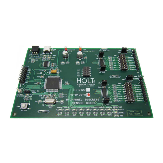
INTRODUCTION This board demonstrates the features of the HI‐8428‐R eight input discrete sensor IC. The HI‐8428‐R is powered from 3.3V ±5% VLOGIC and 12 to 16.5V VDD supply voltages. The device is configured and sensor data read by the SPI serial bus, sensor input thresholds are fixed at Airbus specification levels. The EVM (Evaluation Module) contains a 16 bit, Freescale MC9S12XDT512 MCU, this is used to interface to a terminal emulator and control the HI‐8428‐R. The Holt CD, included with the evaluation kit, contains example source code, providing an easy path for the customer to develop their own control software. A Serial UART output from the MCU provides debug and data messages to be sent to a PC using any terminal emulation program such as Tera Term. The HI‐8428‐R Evaluation Board (shown in the picture below), two HI‐8428‐R devices are mounted on the board so the customer can evaluate SPI daisy chain operation. A bank of LEDs monitors the outputs on either bank of eight sensors. This guide summarizes how to set up and get running quickly. Additional support material is provided on CD‐ROM. KIT CONTENTS This User Guide. HI‐8428‐R Evaluation Board. QSG‐8428‐R Rev. A HOLT INTEGRATED CIRCUITS Oct 2014 2 ... -
Page 3: Demonstration Set-Up
CD with HI‐8428‐R Users Documentation. USB to Mini USB Serial Cable. Demonstration Set‐up SUPPLY VLOGIC SUPPLY HI-8428-R DIP SW From Sensors SENSOR TRIGGER Sensor Inputs MC9S12XD 16 Bit MCU SENSOR LEDs (10) SUPPLY RESET BUTTON HI-8428-R DIP SW DIP SW From Sensors 4MHz Sensor Inputs QSG‐8428‐R Rev. A ... - Page 4 Default Jumper Settings JUMPER POSITION DESCRIPTION J1 ON VLOGIC Link for supply current to U1 (disconnect to measure HI‐8428‐R VLOGIC supply current ) J2 ON VDD Link for supply current to U1 (disconnect to measure HI‐8428‐R VDD supply current ) J13 ON VLOGIC Link for supply current to U2 (disconnect to measure HI‐8428‐R VLOGIC supply current ) J12 ON VDD Link for supply current to U2 (disconnect to measure HI‐8428‐R VDD supply current ) J3 3 U1 Sensor Switch ‘On’ Level Left = GND/Open Right = Supply/Open J6 3 U2 Sensor Switch ‘On’ Level Left = GND/Open Right = Supply/Open n J11 OFF In ON position ‐ holds the Freescale MCU in reset, use this when using an external SPI controller. QSG‐8428‐R Rev. A HOLT INTEGRATED CIRCUITS Oct 2014 4 ...
-
Page 5: Default Switch Settings
Default Switch Settings SW1 POSITION DESCRIPTION SW1, 1‐8 All ON Sensor inputs for U1, Sensors 1‐8, use in combination with J3 SW2, 1‐8 All ON Sensor inputs for U2, Sensors 1‐8, use in combination with J6 SW3, PE2 ON OFF = Boots up in GND/Open mode. LEDs monitor sensors SW3, PE3 ON OFF = Boots up in Supply/Open LEDs monitor sensors SW3, PE4 ON OFF = Boots up with LED counter running SW3, PE5 ON No Function SW4, Reset OFF Press down to reset MCU and reboot software QSG‐8428‐R Rev. A HOLT INTEGRATED CIRCUITS Oct 2014 5 ... - Page 6 GND Ground connection J8 USB Connect to PC to send SPI commands from terminal emulator J9 Debug Header Used for downloading MCU firmware J10 External SPI SPI interface for U1/U2 (Insert jumper J11 when using this) J11 Debug Header Used for downloading MCU firmware LED Functions REF NAME DESCRIPTION LED 1‐8 SENSE 1‐8 LED lights when sensor output is ‘high’, when using the software LED monitor feature. LED 9 BANK1 LED lights when sensors from U1 are being monitored, when using the software LED monitor feature. LED 10 BANK2 LED lights when sensors from U2 are being monitored, when using the software LED monitor feature. LED 11 3V3 LED lights when VLOGIC power is present. LED 12 VDD LED lights when VDD power is present. QSG‐8428‐R Rev. A HOLT INTEGRATED CIRCUITS Oct 2014 6 ...
- Page 7 Initial Board Set up 1. Make sure the board jumpers and switch positions match the default settings listed earlier. Connect a +3.3V power supply to VLOGIC (RED) and 0V to GND terminals. Connect a +12V to +16.5V power supply to VDD (RED) and 0V to GND terminal. The VLOGIC and VDD terminals also supply other components, to measure only the HI‐8428‐R supply currents; remove the jumper for the device for (VDD or VLOGIC) and connect an ammeter across the two terminals; an accurate current measurement can now be made. 2. On power up the LED bank, SENSE[8:1] will light for 1 sec, the software revision is then displayed on the same LEDs, SENSE[8:5] being the most significant digit and SENSE[4:1] being the least significant digit. Boot Up Options 1. Normally control of the HI‐8428‐R devices is through the on board MCU, and interfacing with a terminal emulator. However there are three boot up options selectable that do not need the terminal emulator, these are selected using SW3, see switch table on page 5. 2. The PE2 option sets GND/Open sensor mode for U1 and then monitors the sensor outputs on the Sense 1‐8 LEDs, an illuminated LED means that sensor is Open (High). 3. The PE3 option sets Supply/Open sensor mode for U1 and then monitors the sensors outputs on the Sense 1‐8 LEDs, an illuminated LED means that sensor is at Supply level (High). 4. The PE4 option starts the LED Count Test mode. 5. Options are changed by altering SW3 and hitting the Reset button. 6. When PE2, PE3, PE4 are all ON, then the normal software mode is selected, see next section. QSG‐8428‐R Rev. A HOLT INTEGRATED CIRCUITS Oct 2014 7 ...
-
Page 8: Software Control
Accept the default install destination and click Next. o At the Select Components screen, unselect all options except Additional Plugin = TTXResizeMenu and click Next. o Select the installed language, then click Next. o Accept the default Start Menu folder, then click Next. o Select any desired shortcuts, then click Next. o At the Ready to Install screen, click Install. Run the installed Tera Term program. At the New Connection screen, select (x)Serial and choose the selected COM port, find the correct COM port using Device Manager. 4. Click Setup then Serial Port to open the serial port setup window. Choose the COM port for the mini‐USB connection and then select the following settings: Baud Rate: 115200, Data: 8 bits, Parity: none, Stop: 1 bit, Flow Control: none 5. The evaluation software is pre‐programmed into the MCU at the Holt Applications Support Center. Ensure all SW3 switches are ‘ON’, press the ‘RESET MCU’ button on the board, the software displays a message on the monitor, similar to the screenshot shown below. QSG‐8428‐R Rev. A HOLT INTEGRATED CIRCUITS Oct 2014 8 ... - Page 9 6. Note: If under any circumstances, this software locks up, use the ‘RESET’ key to recover. 7. Press key ‘t’ to perform an LED test. The Sensor1‐8 LEDs and screen should go through a binary count. To set a test data configuration; press key ‘w’ to write 9 configuration bits, enter 1 then 55, as shown in the screen below: QSG‐8428‐R Rev. A HOLT INTEGRATED CIRCUITS Oct 2014 9 ...
- Page 10 8. Press key ‘c’ to read configuration. The values you programmed (test bit 1, config = 0x55) should be displayed as shown in the screen below: 9. When the test bit is set to ‘1’, test data can be placed into the data buffer through the SPI bus, this is a test feature which tests a large portion of the device, but not the comparator and threshold setting circuits. Press key ‘r’ to read data, only the test data should now be read, as shown below: 10. To configure all U1 sensors as GND/Open press key ‘w’ and set test bit to 0, then enter FF. Press ‘c’ to read registers back to the screen and verify that the configuration reads; 0xFF All 8 sensors are now set to detect the GND/Open states. The short cut keys ‘G’ and ‘S’ can also be used the set all sensors to GND/Open and Supply/Open respectively. QSG‐8428‐R Rev. A HOLT INTEGRATED CIRCUITS Oct 2014 10 ...
- Page 11 11. A quick test of the inputs can made using DIP switch SW1, press key ‘G’ to set GND/Open mode, then key ‘l’ and ‘A’. With the jumper SENSOR_BANK_U1 in position 1, set all switches to ON, this sets all inputs to GND level. Now open switch SW1/1, SENSE1 LED should light. Carry on opening the rest of the switches, each corresponding LED should now light. 12. The same test can be done for Supply/Open, set jumper SENSOR_BANK_U1 IN position 3, apply a voltage of 15V to the test point next to J3. Set all switches to OFF, this sets all inputs to Open level. Now close switch SW1/1, SENSE1 LED should light. Carry on closing the rest of the SW1 switches, each corresponding LED should now light. Testing Sense Thresholds 1. In GND/Open mode, VGTHL is 4.5V min and VGTHH is 10.5V max. This can be tested by connecting a voltage source to the Sensor input pin on connectors J4 and J7. Make sure all SW1 DIP switches are in the OFF position. Connect a variable voltage source (initially set to 0V) to J4 pin 1, this tests Sensor 1 of U1. Use the short cut ‘G’ key to program all U1 sensors to GND/Open, press the ‘l’ key and then select ‘0’ for sensor 1, the screen should scroll as shown below, this continually monitors the U1 sensor bank. 2. The screen above is monitoring U1 sensor 1, 0xFE means sensors 2 to 7 bits are at a ‘1’, in GND/Open, and this means Opens are detected (≥10.5V). Because sensor 1 is held at 0V the last bit reads ‘0’ or a Closed state (≤4.5V). Now increase the voltage source up to 9V, increase the voltage slowly, at 10.5V, LED1 on the board should be lit, the screen should now read 0xFF instead of 0xFE. Now decrease the voltage, LED1 should go off before 4.5V is reached. 3. Press any key then press key ‘S’ to set all sensors to Supply/Open mode. Press the ‘l’ key and then select ‘0’ for sensor 1, the screen should scroll as before below but displaying 0x00, LED1‐8 should be off. Again from 0V, slowly increase voltage until LED1 is lit, this voltage should be ≤12V, now decrease the voltage, LED1 should go off before 6V is reached. QSG‐8428‐R Rev. A HOLT INTEGRATED CIRCUITS Oct 2014 11 ...
- Page 12 4. An individual sensor can also be monitored from the hardware trigger output, by connecting to the Sense Trigger test point. This output can be used to measure high and low thresholds by inputting a ramp voltage to the sensor and then monitoring this on an oscilloscope, the test point is used to trigger the oscilloscope of the SPI mother board, when the sensor changes state; so does the level on sensor trigger. Daisy Chained SPI Mode 1. Two HI‐8428‐R devices are provided on the evaluation board, this allows the ‘daisy chained’ feature to be evaluated. U1 and U2 are linked together through the SPI connections; the SO pin of U1 is linked to the SI pin of U2. The software has commands that program and read both devices using this feature. 2. Press key ‘d’ write 1, AA, 1, 55, press key ‘e’, the screen below should be seen. The configuration register of both devices has been set and read back through the daisy chain link. 3. Configure the board with jumpers SENSE BANK_U1 and SENSE BANK_U2 is in the ‘1’ position, press key ‘d’ and program 0, FF, 0, FF, all sensors are now programmed to GND/Open. Set all SW1, 2 switches to ‘ON’. 4. Press key ‘m’, the screen should scroll through, showing the sensor data 0x00 0x00 for each device, set SW1 to 0x55 and SW2 to 0xAA positions and observe the corresponding change on the screen. See example screen below. 5. The ‘k’ command can be used to read just the U2 sensors and monitor these on the SENSE1‐8 LEDs, in the same way the ‘l’ command is used for U1. Press key ‘k’ and then ‘A’ the LEDs should read ‘10101010’ and the BANK2 LED should be lit. QSG‐8428‐R Rev. A HOLT INTEGRATED CIRCUITS Oct 2014 12 ...
-
Page 13: Connecting External Sensors
U1 U2 1 Sensor 1 Sensor 1 2 Sensor 2 Sensor 2 3 Sensor 3 Sensor 3 4 Sensor 4 Sensor 4 5 Sensor 5 Sensor 5 6 Sensor 6 Sensor 6 7 Sensor 7 Sensor 7 8 Sensor 8 Sensor 8 9 GND GND Connection pins for external sensors Lightning Tests The board comes fitted with a 3kΩ resistor on each sensor input; these resistors are not designed to survive a lightning test. If lightning tests are to be performed, please use a board designed for this and with the recommended resistor, contact Holt Support for guidance on this. QSG‐8428‐R Rev. A HOLT INTEGRATED CIRCUITS Oct 2014 13 ... - Page 14 SPI Connector (J10) Pin Label Description Number 2 SO1 SPI Serial Output of U1 4 SEL Select Input of U1 and U2 6 nCS SPI Chip Select for U1 and U2 8 SO SPI Serial Output from U2 10 SI SPI Serial Data Input to U1 12 SCK SPI Serial Clock Input 14 VDD 12 to 16.5V supply 16 3V3 3.3V supply Odd Nos Supply Ground (0V) GND J11 connection pins, for external SPI QSG‐8428‐R Rev. A HOLT INTEGRATED CIRCUITS Oct 2014 14 ...
- Page 15 D o c u m e n t N u m b e r R e v 47pF CASE <Doc> <Rev Code> D a t e : S h e e t Thursday , September 18, 2014 QSG‐8428‐R Rev. A HOLT INTEGRATED CIRCUITS Oct 2014 15 ...
- Page 16 490-5988-1-ND Murata BLM21PG331SN1D Ferrite 220 Ohm @100 MHz 0805 490-1054-1-ND Murata BLM21PG221SN1D Conn Header .100 SGL STR 2Pos Holt On Reset, U1-Logic, U1_VDD, S1012E-02-ND Sullins PEC02SAAN U2_Logic, U2_VDD Conn Header .100 SGL STR 3Pos S1012E-03-ND Sullins PEC03SAAN J3,J6 Conn Header .100 SGL STR 9Pos...
- Page 17 Keystone 5012 Test Point, Orange Insulator, 0.062" 5013K-ND Keystone 5013 Test Point, White Insulator, 0.062" 5012K-ND Keystone 5012 Sense Trigger HI-8428-R 16-SOIC HI-8428-R HI-8428-R SOIC16 U1,U2 IC USB SERIAL FULL UART 20SSOP 768-1129-1-ND FTD FT231XS-R IC, MC9S12XDT512CAA 80 QFP 16-Bit MCU,...
-
Page 18: Revision History
REVISION HISTORY Revision Date Description of Change QSG-8428-R, Rev. 9-12-14 QSG-8428-R, Rev. A 10-1-14 New board (SW1, SW2 location moved on schematic) QSG‐8428‐R Rev. A HOLT INTEGRATED CIRCUITS Oct 2014 18 ...
Need help?
Do you have a question about the HI-8428-R and is the answer not in the manual?
Questions and answers