Table of Contents
Advertisement
Quick Links
HI‐3110 ARINC 825 CAN Bus Controller
Evaluation Board Users Manual
INTRODUCTION
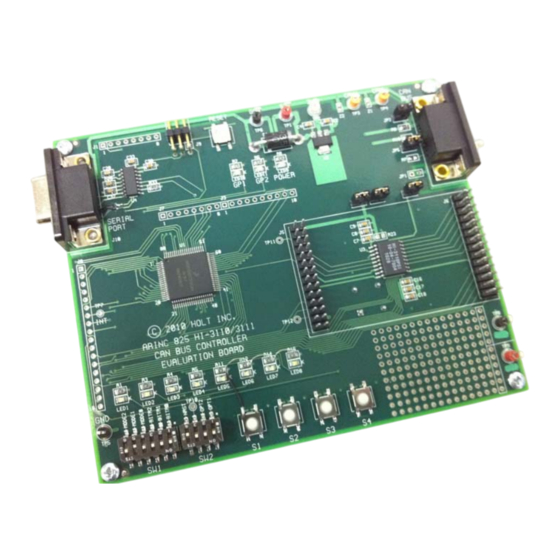
The Holt HI‐3110 ARINC 825 CAN BUS Controller Evaluation Board can be used to evaluate some
of the features of the HI‐3110 CAN Controller with integrated transceiver IC. A Freescale
MC9S12XDT512 microcontroller with 512K flash and 20K RAM communicates with the HI‐3110
through the SPI interface. The board includes switches and LEDs to help navigate the operating
modes and confirm data and status information. A Serial UART port is provided to allow debug
and data messages to be sent to a PC using any terminal program such as Hyper‐terminal.
9/2/2010
Advertisement
Table of Contents

Related Manuals for HOLT HI-3110


Summary of Contents for HOLT HI-3110
- Page 1 HI‐3110 ARINC 825 CAN Bus Controller Evaluation Board Users Manual 9/2/2010 INTRODUCTION The Holt HI‐3110 ARINC 825 CAN BUS Controller Evaluation Board can be used to evaluate some of the features of the HI‐3110 CAN Controller with integrated transceiver IC. A Freescale MC9S12XDT512 microcontroller with 512K flash and 20K RAM communicates with the HI‐3110 through the SPI interface. The board includes switches and LEDs to help navigate the operating modes and confirm data and status information. A Serial UART port is provided to allow debug and data messages to be sent to a PC using any terminal program such as Hyper‐terminal. ...
-
Page 2: Kit Contents
KIT CONTENTS This Users Manual. HI‐3110 Evaluation Board and Schematic HI‐3110 Data Sheet RS‐232 Serial Cable Software version 6 Demonstration Features Transmit Modes for Standard and Extended Frames Receive Modes, polled and interrupt driven Monitor Mode LoopBack Mode Sleep Mode with wake‐up from Button press or CAN data Selectable Bit Rates from 83.3KBPS ‐ 1MBPS Print out the CAN buffers (64) on the serial console Print out the status registers on the serial console Print out the Transmit History FIFOs on the serial console Print out the Error Status registers on the serial console Configuring the INT, STAT and GP1 and GP2 outputs SPI clock frequency selectable from 625KHz – 10MHz. ... -
Page 3: Demonstration Setup
Demonstration Setup The board requires a +5V (0.5A) power supply applied to TP1 and Gnd to TP6. There are two ways to connect the CANL and CANH signals to the CAN Bus. The CANL and CANH Bus signals are available on the two test points on the top right side of the board or from the DB9 connector. Power On Reset For normal operation ensure SW2 – 4 (MRST) is in the open position otherwise the MCU will be held in the reset state. The purpose of this MRST dip switch is to allow easy interfacing of an external MCU to the HI‐3110 such that the SPI signals from the Freescale MCU will be forced into high impedance so as not to conflict with an external MCU. For normal operation keep this switch open and use the RESET button to reset the MCU during testing. ... - Page 4 CAN BUS Bit Rate selection The Bit Rate can be selected by configuring the 3 dip switches in SW1. The program fetches the switch positions once after a power up. S3 S2 S1 Bit Rate 0 0 0 1 MBPS 0 0 1 500 KBPS 0 1 0 250 KBPS 0 1 1 125 KBPS 1 0 0 83.3 KBPS Mode Selection Mode2 Mode1 Mode0 Mode ...
-
Page 5: Board Jumpers
The serial port is optional and provides access to additional status and data information: Software Revision Current Mode CAN Frame data CAN History FIFO data Status Registers data Sleep Mode status Serial Commands Menu A simple menu of commands is provided for resetting the HI‐3110, reading and displaying the HI‐3110 status registers, and a demo how to pass input strings to the program. There are provisions for additional user code to be implemented so custom commands can be developed and easily integrated. UART Serial Port Setup: 115200 Baud, 8 bits, No Parity, No handshaking. At power on reset (POR) the revision of the program will be displayed on the LEDs for two seconds in binary format where LED1 is the LSB. After two seconds they will be turned off then LED7 will flash every second as the main MCU “live” operating indicator. A message will also be sent to the Serial Port . For Receive mode it will be shown as: Holt HI 3110 Demonstration Software Revision: 05 Receive Mode polled Board Jumpers JP1 ‐ CAN BUS connector shield JP2 ‐ CANH 60 ohm termination ‐ Remove this in Monitor mode. JP3 ‐ VDD jumper to U3 VLOGIC. Can be used to measure ICC. JP4 ‐ SPLIT termination voltage filter. JP5 ‐ CANL 60 ohm termination – Remove this in Monitor mode. JP7 ‐ VDD jumper to U3 VDD. Can be used to measure ICC. Users Guide Mode‐0: Board Test ... - Page 6 Mode‐1: Transmit Mode Standard Frames This transmits a standard CAN frame with an incrementing 32‐bit value in the first 4 bytes of the data –field, the last four bytes will be 00. After RESET press the Button‐1 to start the transmissions. A portion of the data field will be copied to the LED1‐LED4’s. They can be seen counting in this mode. Press Button‐1 to stop transmitting and print out the status registers on the serial console. Press Button‐2 to pause the transmission. Press Button‐2 again to transmit one frame again. Press Button‐3 to print out the Transmit History FIFO contents on the serial console. Press Button‐4 to resume transmissions. OPT1 switch= open, Inserts a 400us delay before each transmission. Mode‐2 Receive Mode using Polling method Receive mode is customized to the Transmit mode because it expects the incrementing 32‐bit value in the data‐field to compare with the predicted value starting from count zero. LED1‐4 will reflect the lower nibble of byte3 of the data‐field. OPT1 switch =open, The program will compare the 32‐bit counter value in the data‐field and turn on the RED LED8 and halt if it does not match the expected value. To exit from the halt condition press close the OTP1 switch or press the RESET button. CAN Error Detection While receiving frames if there are any errors detected in the HI‐3110 registers, TEC, REC or ERR, they will be automatically logged on the Serial Port. For example if ERR has a 01 value it would be shown as: ERR: 01. The other two errors will be shown similarly. Button‐1 – Stop receiving CAN messages and print the last 64 CAN frames and the status registers on the serial console. Press Button‐4 to resume receiving CAN Messages. Button‐3 – Put the HI‐3110 into Sleep Mode. Press Button‐4 or send CAN messages in Sleep mode to terminate and re‐enter Normal mode. A message on the serial console will indicate the Sleep Mode and the source to the wake‐up event. Holt HI 3110 Demonstration Software Revision: 06 Receive Mode polling...
- Page 7 SLEEP Mode Entered Detected Wake-up from Button-4 ---> Entering Normal Mode. SLEEP Mode Entered Detected Wake-up from Monitor Mode ---> Entering Normal Mode. REC: 01 ERR: 08 The last line shows a BUS error that was caused when the HI‐3110 was in Sleep Mode and woke up due to a CAN message coming in. The program automatically switches from Sleep Mode to Monitor Mode and the program monitors this status and then reprograms the HI‐3110 for Normal mode before receiving CAN messages again. Mode‐3 Monitor Mode Monitor mode is a simple version similar to Receive mode but just captures the CAN data without providing an acknowledge bit on the Bus. Press Button‐1 to stop receiving CAN messages and print the last 64 CAN frames and the HI‐ 3110 status registers on the serial console. Press Button‐4 to resume reception of CAN Messages. ...
- Page 8 Button‐1 – Stop receiving CAN messages and prints the last 64 CAN frames and the HI‐3110 status registers on the serial console. Press Button‐4 to resume receiving CAN Messages. Mode‐5 Transmit Extended Frames This is the same as Transmit Mode‐1 but with Extended Frame format. Mode‐6 Receiver Interrupt Mode This is very similar to normal Receive mode‐2 but without Sleep Mode. The main purpose is to demonstrate how to use interrupts to received the CAN Bus data in the background. Press Button‐1 to stop receiving CAN messages and print the last 64 CAN frames and the HI‐ 3110 status registers on the serial console. Press Button‐4 to resume reception of CAN messages. Mode‐7 Serial Commands Menu After a power on reset, a simple text menu will be displayed on the serial console: ************** HOLT HI‐3110 Serial Console Commands ************* Input String Demo 0 Reset 1 Status Register Read 2 Filter Incrementing 3 Enter Selection:2 Enter “1” to generate a hardware reset to the HI‐3110. Enter “2” for the status register read and display: CTR0 =80 CTR1 =00 BTR0 =00 BTR1 =00 TEC =00 REC =00 MESSTAT =00 ...
-
Page 9: Software Description
ERR =00 INTF =00 INTE =82 STATFE =00 GPINE =00 TIMERUB =0D TIMERLB =66 Enter “3” to run a test program to increment filter data. This is currently not used anywhere. Software Description The software project is built with Freescale’s Codewarrior version 5.9.0 using the free version which is limited to 32K code size. The current code size is approximately 10.5K. The main functions are in main.c and the lower level HI‐3110 drivers are in the 3110Driver.c file. Project Files Source Files main.c Main code 3110Driver.C SPI low‐level drivers for the HI‐3110 Peripherals.c GPIO, PLL frequency setup and SPI configuration BoardTest.c Board Test functions Uart.c Low‐level UART drivers datapage.c ... - Page 10 MCU Clock and SPI Frequency The Freescale MC9S12XDT512 (MCU) uses a 4MHz crystal for operation and the built‐in PLL is used to multiply this by 20 to achieve an 80MHz system clock. This system clock is divided by two for a 40MHz Bus Clock which is used internally for the MCU peripherals. The PLL is programmed to multiply by 20 by this line: SYNR = 9; // 80Mhz PLL system clock The SPI frequency is set by this line of code: SPI0BR = SPI_5MHZ; // SPI CLK = 5MHz (see “peripherals.c” for other rates) Timer Interrupt and timings A 100us Timer0 interrupt supports basic timings. A number of predefined constants are provided to allow some common delays passed into the Delay100us() function: #define K_1MS 10 #define K_10MS 100 #define K_100MS 1000 #define K_1SEC 10000 Usage: Delay100us(K_1SEC); // delay for one second A one second interrupt handler in the TIMER_ISR is provided. Any code placed here will automatically get executed every second. if (!count100us) { // 1 second scheduler count100us = K_1SEC; if(ON==g_ledFlashBool) // Flash the LED8 if enabled LED8 ^= TOGGLE; // Alive 1 second blink } HI‐3110 Interrupts ...
- Page 11 There are several functions to read in a single byte from the 3110 SPI port, write a command to the 3110 SPI port and a few others which read or write a command plus a multiple number of bytes. For example the function below is the basic function to write out a command plus one byte of data to the 3110 SPI port. // Write SPI Command with a Value to HI-3110 void W_CommandValue (uint8 cmd, uint8 value){ uint8 dummy; SPI0CR1 = SPI0CR1 & ~SPI0CR1_SSOE_MASK; // disable auto /SS output, reset /SS Output SPI0CR2 = SPI0CR2 & ~SPI0CR2_MODFEN_MASK; // disable auto /SS output, reset SPI0 Mode SPI0_nSS = 0;...
- Page 12 SPI0CR2 = SPI0CR2 | SPI0CR2_MODFEN_MASK; // enable auto /SS output, set SPI0 Mode Fault This function is used to transmit a command byte followed by a multiple number of data bytes contained into the array passed by the pointer. In this case it’s used to load the SPI Write Transmit FIFO command byte 0x12 and the frame data bytes. void TransmitStandardFrame(uint8 *TXBuffer) uint8 static ByteCount,dummy; SPI0CR1 = SPI0CR1 & ~SPI0CR1_SSOE_MASK; // disable auto /SS output, reset /SS Output SPI0CR2 = SPI0CR2 &...
-
Page 13: Transmit Mode
GPI and GP2 The HI‐3110 general purpose output pins can be configured to output status information described in the GPINE register. The program configures these differently depending on the mode and the LED10 and LED11 will turn on when these are at a logic low. LEDs LED1‐LED8 The group of eight LEDs (LED1‐LED8) are supported by a function in the program since LED1‐ LED4 are low true logic whereas LED5‐LED8 are high true logic. Usage: LED_CTL(LED_1,OFF); // turns off LED1 Usage: LED_CTL(LED_1,ON); // turns on LED1 TRANSMIT MODE Select transmit mode from the SW1 dip switches and Press Button‐1 after a POR to start transmitting frames. The transmit function configures the HI‐3110 for normal mode at the CAN Bus rate according to the Bit Rate dip switches. A frame is composed of a predefined header “T8Header[]” and eight bytes for the data‐field. For Mode‐ 5, Extended Frame Format a different header is used “T8HeaderExt”. The program concatenates a 32‐bit incrementing counter “BigCounter.Word32” to the header data and loads this into a transmit buffer “TXBuffer” before loading the FIFO with the frame before each transmission. For debugging purposes there is a special function “getRegStatus()” which will read out the status registers and load them into an array “DebugArray[]” for viewing if Button‐1 is pressed. The transmit function writes to the FIFO’s until it is filled then waits until the FIFO becomes not full before loading the next frame by reading the TXFULL status bit in the status register. RECEIVE MODE Select receive mode from the SW1 dip switches and the program will go directly into this mode after a power on reset. The receive mode reads in a frame by first examining the receive FIFO empty bit in the status register. Received frames are compared with the expected 32‐bit ... - Page 14 frames of data captured in the array and the set of status registers on the Serial Port. An asterisk will be placed at the beginning of the frame of the last message received as shown below: CAN: 00 BF 9D 47 20 00 00 08 00 00 4C 53 00 00 00 02 CAN: 00 C0 16 47 20 00 00 08 00 00 4C 54 00 00 00 02 CAN: 00 C0 8F 47 20 00 00 08 00 00 4C 55 00 00 00 02 CAN: 00 C1 08 47 20 00 00 08 00 00 4C 56 00 00 00 02 CAN: 00 C1 81 47 20 00 00 08 00 00 4C 57 00 00 00 02 CAN: 00 C1 FA 47 20 00 00 08 00 00 4C 58 00 00 00 02...
- Page 15 {W_FILTER7, 0x47,0x00, 0x00, 0x00, 0x00,0x00}, // Filter 7 }; // CAN Bus acceptance masks unsigned const char Masks[8][7] ={ // Mask data {W_MASK0, 0xFF,0x00, 0x00, 0x00, 0x00,0x00}, // Mask 0 {W_MASK1, 0xFF,0x00, 0x00, 0x00, 0x00,0x00}, {W_MASK2, 0xFF,0x00, 0x00, 0x00, 0x00,0x00}, {W_MASK3, 0x00,0x00, 0x00, 0x00, 0x00,0x00}, // Accept everything with filter 3 {W_MASK4, 0xFF,0x00, 0x00, 0x00, 0x00,0x00}, {W_MASK5, 0xFF,0x00, 0x00, 0x00, 0x00,0x00}, {W_MASK6, 0xFF,0x00, 0x00, 0x00, 0x00,0x00}, {W_MASK7, 0xFF,0x00, 0x00, 0x00, 0x00,0x00}, // Mask 7 }; This example code is setup to filter on ID28‐ID20 = 0x47. The transmitter already transmits this value so by default the messages will be received. All other messages other than 0x47 will be except by filter‐3 . Refer to the datasheet page 38 and example code for the bit assignments of the other 5 bytes in these arrays. Freescale MC9S12XDT512xxx Development Tools The Freescale microcontroller data sheet and other documentation can be found at this link: http://www.freescale.com/webapp/sps/site/prod_summary.jsp?code=S12XD&tid=16bhp A Free 32K limited version of the Code Warrior IDE from Freescale is available: http://www.freescale.com/webapp/sps/site/prod_summary.jsp?code=CW‐HCS12X&fsrch=1 The US Multilink debugger cable used for this project is: http://www.freescale.com/webapp/sps/site/prod_summary.jsp?code=USBMULTILINKBDM&par entCode=S12XD&fpsp=1 ...
Need help?
Do you have a question about the HI-3110 and is the answer not in the manual?
Questions and answers