Neoway N58 Hardware User's Manual
Industrial 4g module
Hide thumbs
Also See for N58:
- Hardware user's manual (88 pages) ,
- Hardware user's manual (87 pages) ,
- Hardware user's manual (45 pages)
Table of Contents
Advertisement
Advertisement
Table of Contents

Related Manuals for Neoway N58


Summary of Contents for Neoway N58
- Page 1 Hardware User Guide Issue 1.0 Date 2019-12-16...
- Page 2 THIS GUIDE PROVIDES INSTRUCTIONS FOR CUSTOMERS TO DESIGN THEIR APPLICATIONS. PLEASE FOLLOW THE RULES AND PARAMETERS IN THIS GUIDE TO DESIGN AND COMMISSION. NEOWAY WILL NOT TAKE ANY RESPONSIBILITY OF BODILY HURT OR ASSET LOSS CAUSED BY IMPROPER OPERATIONS. THE INFORMATION IN THIS DOCUMENT IS SUBJECT TO CHANGE WITHOUT NOTICE DUE TO PRODUCT VERSION UPDATE OR OTHER REASONS.
-
Page 3: Table Of Contents
Scope ..............................vii Audience ............................vii Change History ..........................vii Conventions ............................vii Related Documents .......................... viii 1 About N58 ....................9 1.1 Product Overview ......................... 9 1.2 Block Diagram ..........................10 1.3 Basic Features ..........................11 2 Module Pins ..................... 13 2.1 Pad Layout .......................... - Page 4 6.2 Label ............................62 6.3 Packing ............................62 6.3.1 Reel ........................... 62 6.3.2 Moisture ..........................64 7 Mounting N58 Onto Application PCB ............65 7.1 Bottom Dimensions ........................65 7.2 Application Foot Print ......................... 66 7.3 Stencil ............................66 7.4 Solder Paste ..........................66 7.5 SMT Furnace Temperature Curve ....................
- Page 5 Table of Figures Table of Figures Figure 1-1 Block Diagram ........................ 10 Figure 2-1 N58 pin definition ......................13 Figure 3-1 Recommended design 1 ....................22 Figure 3-2 Recommended design 2 ....................22 Figure 3-3 Recommended design 3 ....................23 Figure 3-4 Reference design of startup controlled by button ............
- Page 6 Figure 6-2 N58 label ......................... 62 Figure 7-1 Bottom dimensions of N58 (Unit: mm) ................65 Figure 7-2 Recommended footprint of N58 application PCB (Unit: mm) ......... 66 Figure 7-3 SMT furnace temperature curve ..................67 Copyright © Neoway Technology Co., Ltd...
- Page 7 Table 4-4 N58 ESD protection ......................57 Table 5-1 Operating Bands of N58 ....................58 Table 5-2 RF transmit power and RX sensitivity of N58..............59 Table 5-3 GNSS Feature ........................59 Table 5-4 WLAN/BT TX power and RX sensitivity ................60...
-
Page 8: About This Document
About This Document Scope This document is applicable to N58 series. It defines the features, indicators, and test standards of the N58 module and provides a reference for the hardware design of each interface. Audience This document is intended for system engineers (SEs), development engineers, and test engineers. -
Page 9: Related Documents
N58 Hardware User Guide About This Document Related Documents Neoway_N58_Datasheet Neoway_N58_Product_Specifications Neoway_N58_AT_Command_Mannual Neoway_N58_EVK_User_Guide Copyright © Neoway Technology Co., Ltd viii... -
Page 10: About N58
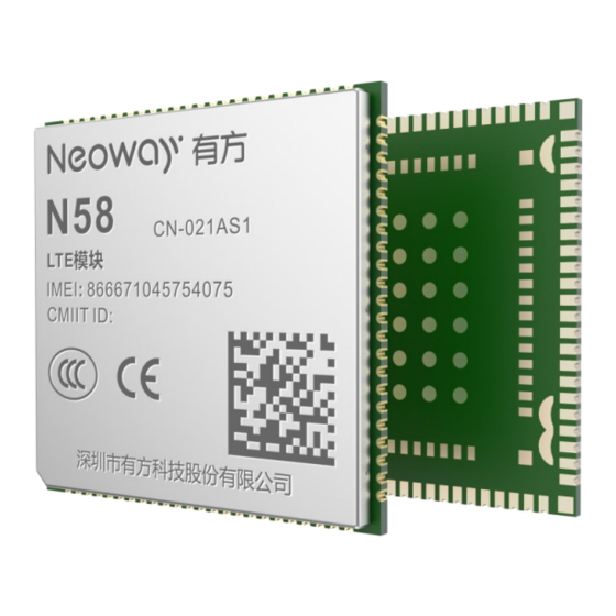
Chapter 1 About N58 1 About N58 N58 is an industrial 4G module that is developed on Spectrum chipset. Its dimensions are 30 x 28 mm x 2.6 mm. This high-performance data transmission module supports GSM, FDD LTE, TDD LTE (Cat 1) network modes, provides various hardware interfaces, supports audio and video functions and BT connectivity, and optionally supports GNSS. -
Page 11: Block Diagram
N58 Hardware User Guide Chapter 1 About N58 1.2 Block Diagram N58 consists of the following functionality units: Baseband ⚫ 26MHz crystal oscillator ⚫ Power management unit ⚫ RF section ⚫ Digital interfaces (USIM, I2C, ADC, UART, USB, SDIO) ⚫... -
Page 12: Basic Features
One 12-bit ADC interface, detectable voltage ranging from 0.1 to 1.7V. One SDIO interface, used for SD card One 1PPS interface One I2C interface, host mode only 3GPP Release 13 AT commands Neoway extended commands PDU, TXT Copyright © Neoway Technology Co., Ltd... - Page 13 N58 Hardware User Guide Chapter 1 About N58 Data PPP, RNDIS, ECM Protocol TCP, UDP, MQTT, FTP/FTPS, HTTP/HTTP(S), SSL, TLS Certification approval CCC, SRRC, RoSH, CE * indicates functions that will be supported in the future. Copyright © Neoway Technology Co., Ltd...
-
Page 14: Module Pins
N58 Hardware User Guide Chapter 2 Module Pins 2 Module Pins There are 192 pins on N58 and their pads are introduced in LGA + LCC package. 2.1 Pad Layout Figure 2-1 shows the pad layout of N58. Figure 2-1 N58 pin definition... -
Page 15: Pin Description
27, 28, 29 =4.2V Supply at most 2A current supply input Used only for level shifting 1.8V power =1.8V norm VDD_1P8 and IO power supply. output =50 mA Leave this pin floating if it Copyright © Neoway Technology Co., Ltd... - Page 16 UART2_TX Data transmitting P3 commissioning. Leave this pin floating if it is not used. Used data transmission and module UART2_RX Data receiving commissioning. Leave this pin floating if it is not Copyright © Neoway Technology Co., Ltd...
- Page 17 USIM1_VCC through a 10 kΩ pull-up resistor. USIM1 clock USIM2_CLK output USIM2_RESET USIM1 reset USIM2_DET USIM1 detect USB interface 3.4V Route DM and DP signals Charging voltage USB_VBUS 5.2V, TYP: differential mode, check control impedance of 90Ω Copyright © Neoway Technology Co., Ltd...
- Page 18 SPI chip select LCD_SPI_CLK SPI clock Data LCD_SPI_SDC command signal LCD_SPI_SIO Data input/output P3 LCD_SPI_SEL Select signal 1.8V DC power VDD_LCD Max current: 200mA supply RGB LED input LED_K0 minus LED_K1 RGB LED input Copyright © Neoway Technology Co., Ltd...
- Page 19 Leave this pin floating if it SDC2_DATA_1 SDIO data bit 1 is not used. Leave this pin floating if it SDC_DET SDC detect is not used. VDD_SDCPULL 1.8V power Max current: 150mA Copyright © Neoway Technology Co., Ltd...
- Page 20 Leave this pin floating if it GNSS_LNA_EN enable is not used. power It can be connected to a supply, 1.5V to - cell battery VRTC_GPS 3.6V, typical supercapacitor value 3.0V provides a power source Copyright © Neoway Technology Co., Ltd...
- Page 21 Leave this pin floating if it is not used. 9, 10, 107 -111, 116 -120, 124 - Leave this pin floating if it RESERVED Reserved 127, 144, 145, 148 is not used. -154 Copyright © Neoway Technology Co., Ltd...
-
Page 22: Application Interfaces
The power supply design covers two parts: schematic design and PCB layout. Schematic Design N58 supports a power supply of 3.4V to 4.2V (3.8 V typically, supplied by battery) Figure 3-1 shows the schematic design recommended. Copyright © Neoway Technology Co., Ltd. All rights reserved. -
Page 23: Figure 3-1 Recommended Design 1
Figure 3-2 Recommended design 2 VIN (3.8V) VBAT 10 μF 0.1 μF 470 μF 33 pF 100pF 10 μF 0.1 μF Ω 100 k PWR_EN Ω Ω 10 k Copyright © Neoway Technology Co., Ltd. All rights reserved. -
Page 24: Figure 3-3 Recommended Design 3
Its voltage rating should be larger than 1.5 times the voltage across the power supply. Place a bypass capacitor of low-ESR close to the module to filter out high-frequency jamming ⚫ from the power supply. Copyright © Neoway Technology Co., Ltd. All rights reserved. -
Page 25: Vdd_1P8
2A. Ensure low resistance of power supply trace in design to avoid voltage drop. Never use a diode to make the drop voltage between a higher input and module power. Otherwise, Neoway will not provide a warranty for product issues caused by this. In this situation, the diode will obviously decrease the module performances, or result in unexpected restarts, due to the forward voltage of the diode will vary greatly in different temperature and current. -
Page 26: Figure 3-4 Reference Design Of Startup Controlled By Button
Figure 3-6 Reference design of automatic start once powered up PWRKEY_N kΩ N58 module Startup Process After powering on the VBAT pin, input a negative pulse for longer than 50 ms at PWRKEY_N to start Copyright © Neoway Technology Co., Ltd. All rights reserved. -
Page 27: Figure 3-7 Startup Process
PWRKEY_N is used to hardware power off the module. When the module is working, inputting negative pulses for more than 2 seconds to PWRKEY_N can trigger the power-off state of the module. Figure 3-10 shows the hardware shutdown timing. Copyright © Neoway Technology Co., Ltd. All rights reserved. -
Page 28: Reset_N
If you use a 1.8V/2.8V/3.0V IO system, it is recommended to add a triode to separate it. Refer to the following designs. To reset the module through a high level, refer to Figure 3-5. Figure 3-9 Reset controlled by button 1 kΩ RESET_N N58 module Copyright © Neoway Technology Co., Ltd. All rights reserved. -
Page 29: Psm_Wakeup
Figure 3-10 Reset circuit with triode separating RESET_N VCC_XPX N58 module VDD_1P8 In a circuit shown in Figure 3-10, VDD_EXT=1.8V/2.8V/3.0V, R2=4.7KΩ. The following figure shows the reset process of N58. Figure 3-11 N58 reset process VBAT RESET_N 50ms Active Inactive 3.2.3 PSM_WAKEUP... -
Page 30: Usb
Leave this pin floating if it is not used. USB can be used to download firmware for N58 and establish data communication for commissioning. The module can be used as a USB Device. It is an option for customers. The recommended USB circuit is shown in Figure 3-12. -
Page 31: Uart
N58 provides pins to configure three UART interfaces, two of which support hardware flow control. The UART interfaces support 2 Mbps at most. The level at the interfaces is 1.8V. Figure 3-13 shows the reference design of the UART interface. -
Page 32: Figure 3-13 Uart Connection
EN is the enable pin, which works at a voltage of greater than VL-0.2V. In the above circuit, the ⚫ EN pin is connected to VDD_1P8 and the level shifter is always working. Copyright © Neoway Technology Co., Ltd. All rights reserved. -
Page 33: Usim
USIM1 clock output USIM1_RESET 38 USIM1 reset USIM1_DET USIM1 detect USIM2_VCC USIM1 power output Compatible with 1.8 V/3 V UIM card USIM2_DATA DIO USIM data IO It should be connected to USIM1_VCC Copyright © Neoway Technology Co., Ltd. All rights reserved. -
Page 34: Figure 3-16 Reference Design Of Usim Card Interface
USIM1 reset USIM2_DET USIM1 detect N58 provides pins to configure two USIM card interfaces and supports dual-SIM single standby. The two interfaces are automatically compatible with 1.8V/3V USIM cards. See Figure 3-16. Figure 3-16 Reference design of USIM card interface 20Ω... -
Page 35: Sdio
SDC2 is a dual-voltage SD 3.0 interface, which supports a clock frequency of up to 25MHz. It is compatible with DS only. Figure 3-17 shows the reference design of the SDIO interface. Copyright © Neoway Technology Co., Ltd. All rights reserved. -
Page 36: Figure 3-17 Sdio Connection
Spacing between DATA traces should be larger than 2 times trace width. ⚫ Control the impedance for each SDIO trace to 50Ω. ⚫ The following figures and table shows the timing and parameters of SDR modes. Copyright © Neoway Technology Co., Ltd. All rights reserved. -
Page 37: Spi
SPI_CLK Clock signal SPI_MISO Master input SPI_MOSI Master output SPI_CS_N Chip select The SPI interface supports 1.8 V and only master mode. The following figures show the SPI connection and timing. Copyright © Neoway Technology Co., Ltd. All rights reserved. -
Page 38: I2C
Clock high time t(cl) Clock low time t(mov) Output valid time -5.0 t(mis) Input set-up time t(mih) Input hold time 3.3.6 I2C Signal Function Remarks I2C_SDA I2C data I2C_SCL I2C clock Copyright © Neoway Technology Co., Ltd. All rights reserved. -
Page 39: Audio Interface
2.2kΩ 2.2kΩ I2C_SCL I2C_SDA DATA Figure 3-22 I2C timing 3.4 Audio Interface N58 provides a few of audio input/output interfaces to meet your demands for the audio function. 3.4.1 Analog Audio Input Interfaces Signal Function MIC1_P MIC input plus MIC1_N MIC input minus N58 supports one MIC input. -
Page 40: Figure 3-23 Reference Design 1 Of Differential Mic Input
MICP and MICN traces should comply with the differential rules. ⚫ On the PCB, connect the ground of capacitors and the ground of the audio component to the ⚫ main ground. Keep them 3x widths away from other signal traces. Copyright © Neoway Technology Co., Ltd. All rights reserved. -
Page 41: Analog Audio Output Interfaces
The audio signal traces should be wide enough on the PCB to bear large current when audios ⚫ are output at the highest volume. Isolate the traces from digital signals and clocks as well as Copyright © Neoway Technology Co., Ltd. All rights reserved. -
Page 42: Lcd And Cam Interfaces
139 PI MIPI RGB LED input minus LED_K1 140 PI RGB LED input minus LED_K2 141 PI RGB LED input minus Figure 3-25 Reference design of LCD interface Schematic Guidelines: TBD Copyright © Neoway Technology Co., Ltd. All rights reserved. -
Page 43: Camera
The module provides one ADC channel, and the input voltage ranges from 0.1 V to 1.7 V. The ADC interface supports the highest precision of 12 bit and it can be used for temperature detection and other checks. For details, see Neoway_N58_AT_Command Manual. Copyright © Neoway Technology Co., Ltd. All rights reserved. -
Page 44: Dtr
Enter sleep mode at high level Exits from sleep mode at low level Pull DTR low Whether the module Processing current is in idle state services Enter sleep mode and disable all interfaces Copyright © Neoway Technology Co., Ltd. All rights reserved. -
Page 45: Figure 3-30 Incoming Call Service Process
Figure 3-31 Outgoing call service process Sleep mode Initiate an outgoing service MCU pulls SLEEP pin high Enable UART and process outgoing service Complete service Wait till service is processing? processed MCU pulls SLEEP pin Copyright © Neoway Technology Co., Ltd. All rights reserved. -
Page 46: Netlight
Do not use NET_LIGHT to drive the LED indicator directly since it outputs a high level of 1.8V. It is recommended to drive the LED indicator by controlling a triode. Figure 3-33 Driving LED with a triode module 470Ω 4.7 kΩ NETLIGHT 10 kΩ Copyright © Neoway Technology Co., Ltd. All rights reserved. -
Page 47: Ring
Add an ESD component to protect USB_BOOT in a circuit. The following figure shows the reference design of this pin. Copyright © Neoway Technology Co., Ltd. All rights reserved. -
Page 48: Vrtc_Gps And Vrtc
Otherwise, the GPS is cold started every time. Figure 3-37 shows the reference design of the VRTC power supply. Copyright © Neoway Technology Co., Ltd. All rights reserved. -
Page 49: Gpio
Leave this pin floating if it is not used. GPIO_3 GPIO with interrupt Leave this pin floating if it is not used. N58 provides 3 GPIO pins, all of which support interrupt. Copyright © Neoway Technology Co., Ltd. All rights reserved. -
Page 50: Gnss Enable Interface
Leave this pin floating if it is not used. Control the enable of external GPS_LAN. 3.6.9 Keypad interfaces N58 supports the matrix keyboard (4x3). Key pressing and releasing can be detected. It can detect the composition of any two keys. Signal... -
Page 51: Rf Interface
BT antenna 3.7.1 ANT Interface ANT BT and GNSS antenna of N58 require a characteristic impedance of 50 Ω. You should control the impedance of the traces between the pins and antenna to ensure the RF performance. An impedance matching circuit, such as the L network, split capacitor network, and pi network is mandatory in between. -
Page 52: Figure 3-41 Pi Network
PCB under the RF solder pad. Figure 3-42 Recommended RF PCB design Note the distance between ANT and ANT_GNSS in case of EMI jamming to each other. ⚫ Copyright © Neoway Technology Co., Ltd. All rights reserved. -
Page 53: Ant_Gnss Interface
Reference design of active GNSS antenna After the antenna receives GNSS satellite signals, the LNA amplifies the signals first and then transmits them to the ANT_GNSS of N58 through feeder and PCB traces. Figure 3-44 shows a reference design of the active GNSS antenna. -
Page 54: Ant_Bt Interface
Otherwise, these two parts will jam each other, lowing the RF performance. 3.7.3 ANT_BT Interface The 94th pin of the N58 module is shared by WLAN and Bluetooth. It has a characteristic impedance of 50Ω. For the design and requirements of the WLAN antenna and Bluetooth antenna, see 3.7.1. -
Page 55: Figure 3-45 Specifications Of Mm9329-2700Ra1
PCB after the design phase is completed. They are used only for 2.4G Wi-Fi or Bluetooth because they cannot cover wide frequencies. The following figure shows the layout of the 2.4G ceramic chip antenna. SLDA52-2R540G-S1TF is used as an example. Copyright © Neoway Technology Co., Ltd. All rights reserved. -
Page 56: Figure 3-47 Antenna Layout
5 Space between the antenna and ground area. Figure 3-48 shows the layout of this area. Figure 3-48 Layout around the antenna For more details, refer to the antenna manuals and other documents. Copyright © Neoway Technology Co., Ltd. All rights reserved. -
Page 57: Electric Feature And Reliability
Chapter 4 Electric Feature and Reliability 4 Electric Feature and Reliability This chapter describes the electric features and reliability of N58, including the current and voltage of each power pin, operating and storage temperature ranges, and ESD protection features. 4.1 Electric Features... -
Page 58: Temperature Features
Table 4-4 N58 ESD protection Testing Point Contact Discharge Air Discharge VBAT ± 8KV ± 15KV ± 8KV ± 15KV ± 8KV ± 15KV Cover ± 8KV ± 15KV Others ± 2KV ± 4KV Copyright © Neoway Technology Co., Ltd. All rights reserved. -
Page 59: Rf Features
N58 Hardware User Guide Chapter 5 RF Features 5 RF Features N58 supports network modes including GSM, FDD LTE, TDD LTE (Cat 1), supports wireless connectivities of WLAN and BT, and optionally supports GNSS. This chapter describes the RF features of N58. -
Page 60: Tx Power And Rx Sensitivity
N58 Hardware User Guide Chapter 5 RF Features 5.2 TX Power and RX Sensitivity Table 5-2 RF transmit power and RX sensitivity of N58 Band TX Power RX Sensitivity ≤-108dBm GSM850 33 dBm+2/-2dBm ≤-108dBm EGSM900 33dBm+2/-2dB ≤-108dBm DCS1800 30dBm+2/-2dB ≤-108dBm... -
Page 61: Wlan/Bt Features
Table 5-4 WLAN/BT TX power and RX sensitivity Receiving Operating Bands Rate Transmit power Sensitivity 802.11b (2.4G) 1/2/5.5/11Mbps 6/9/12/18/24/36Mbps 802.11g (2.4G) 48/54Mbps MCS0~MCS4 802.11n (2.4G, 20MHz) MCS5~MCS7 GFSK π/4-DQPSK Bluetooth 8-DPSK Copyright © Neoway Technology Co., Ltd. All rights reserved. -
Page 62: Mechanical Features
N58 Hardware User Guide Chapter 6 Mechanical Features 6 Mechanical Features This chapter describes the mechanical features of N58. 6.1 Dimensions Figure 6-1 N58 dimensions (Unit: mm) Copyright © Neoway Technology Co., Ltd. All rights reserved. -
Page 63: Label
The material and surface finishing must comply with RoHS directives. ⚫ 6.3 Packing N58 modules are packed in sealed bags on delivery to guarantee a long shelf life. Follow the same package of the modules again in case of opened for any reason. 6.3.1 Reel N58 in mass production is delivered in the following packaging. - Page 64 N58 Hardware User Guide Chapter 6 Mechanical Features Tape dimensions Copyright © Neoway Technology Co., Ltd. All rights reserved.
-
Page 65: Moisture
Chapter 6 Mechanical Features Reel dimensions 6.3.2 Moisture N58 is a level 3 moisture-sensitive electronic elements, in compliance with IPC/JEDEC J-STD-020 standard. If the module is exposed to air for more than 48 hours at conditions not worse than 30°C/60% RH, bake it at a temperature higher than 90 degrees for more than 12 hours before SMT. -
Page 66: Mounting N58 Onto Application Pcb
N58 Hardware User Guide Chapter 7 Mounting N58 Onto Application PCB 7 Mounting N58 Onto Application PCB This chapter describes the package of N58, the recommended footprint of the application PCB, and SMT specifications. 7.1 Bottom Dimensions Figure 7-1 Bottom dimensions of N58 (Unit: mm) -
Page 67: Application Foot Print
N58 Hardware User Guide Chapter 7 Mounting N58 Onto Application PCB 7.2 Application Foot Print Figure 7-2 Recommended footprint of N58 application PCB (Unit: mm) 7.3 Stencil The recommended stencil thickness is at least 0.12 mm to 0.15 mm. 7.4 Solder Paste The quality of the solder joint depends on the solder paste volume and the PCB flatness. -
Page 68: Smt Furnace Temperature Curve
Neoway will not provide a warranty for heat-responsive element abnormalities caused by improper temperature control. For information about cautions in N58 storage and mounting, refer to Neoway Module Reflow Manufacturing Recommendations. When manually desoldering the module, use heat guns with great opening, adjust the temperature to 245 degrees (depending on the type of the solder paste), and heat the module till the solder paste is melt. -
Page 69: Safety Recommendations
⚫ with other electronic equipment. Please follow the requirements below in application design: Do not disassemble the module without permission from Neoway. Otherwise, we are entitled to ⚫ refuse to provide further warranty. Please design your application correctly by referring to the HW design guide document and our ⚫... -
Page 70: Conformity And Compliance
Follow the regulations of the countries when storing, applying, and discarding it. REACH This product complies with the halide-free requirements for PCB regulated in the EN61249-2-21 standard and JCPA-ES-01 2003. Copyright © Neoway Technology Co., Ltd. All rights reserved. -
Page 71: Bom
N58 Hardware User Guide B BOM Copyright © Neoway Technology Co., Ltd. All rights reserved. -
Page 72: Abbreviation
Clear to Send Direct Current Digital Cellular System Digital Input Digital Input/Output Downlink Digital Output DPSK Differential Phase Shift Keying DQPSK Differential Quadrature Phase Shift Keying Discontinuous Reception Data Terminal Ready Copyright © Neoway Technology Co., Ltd. All rights reserved. - Page 73 Liquid Crystal Display Light Emitting Diode Land Grid Array Long Term Evolution Microcontroller Unit MIPI Mobile Industry Processor Interface Printed Circuit Board Personal Communications Service Pulse Width Modulation QVGA Quarter Video Graphics Array Copyright © Neoway Technology Co., Ltd. All rights reserved.
- Page 74 Time Division Duplex UART Universal asynchronous receiver-transmitter Uplink Universal Serial Bus USIM Universal Subscriber Identity Module VBAT Battery Voltage VSWR Voltage Standing Wave Ratio Wi-Fi Wireless Fidelity WLAN Wireless Local Area Networks Copyright © Neoway Technology Co., Ltd. All rights reserved.
Need help?
Do you have a question about the N58 and is the answer not in the manual?
Questions and answers