Neoway N58 Hardware User's Manual
Hide thumbs
Also See for N58:
- Hardware user's manual (87 pages) ,
- Hardware user's manual (45 pages) ,
- Hardware user's manual (74 pages)
Table of Contents
Advertisement
Quick Links
Advertisement
Table of Contents

Related Manuals for Neoway N58


Summary of Contents for Neoway N58
- Page 1 Hardware User Guide LTE Cat.1 Module Issue 2.8 Date 2023-03-16...
- Page 2 THIS GUIDE PROVIDES INSTRUCTIONS FOR CUSTOMERS TO DESIGN THEIR APPLICATIONS. PLEASE FOLLOW THE RULES AND PARAMETERS IN THIS GUIDE TO DESIGN AND COMMISSION. NEOWAY WILL NOT TAKE ANY RESPONSIBILITY OF BODILY HURT OR ASSET LOSS CAUSED BY IMPROPER OPERATIONS. THE INFORMATION IN THIS DOCUMENT IS SUBJECT TO CHANGE WITHOUT NOTICE DUE TO PRODUCT VERSION UPDATE OR OTHER REASONS.
-
Page 3: Table Of Contents
5.4.2 Analog Audio Output Interfaces ..................54 5.5 Video Interfaces ......................... 57 5.5.1 LCD ........................... 57 5.5.2 Camera ..........................57 5.6 Other Functional Interfaces ......................58 5.6.1 ADC ........................... 58 5.6.2 NET_LIGHT ........................58 Copyright © Neoway Technology Co., Ltd. All rights reserved. - Page 4 8.2 Labeling ............................79 8.3 Packaging ........................... 79 8.3.1 Reel ........................... 80 8.3.2 Moisture Sensitivity Level ....................81 9 Mounting N58 onto Application Board ............. 82 9.1 N58 PCB Package ........................82 9.2 Application PCB Package ......................83 9.3 Stencil ............................84 9.4 Solder Paste ..........................
- Page 5 Figures Figures Figure 2-1 Block diagram ......................... 15 Figure 4-1 Pad layout of N58 (top view) ..................19 Figure 5-1 Voltage drop of the power supply................... 30 Figure 5-2 Recommended power supply design 1 ................30 Figure 5-3 Recommended power supply design 2 ................31 Figure 5-4 Recommended power supply design 3 ................
- Page 6 Figure 8-1 Top and side view dimensions (unit: mm) ............... 78 Figure 8-2 N58 labels ........................79 Figure 9-1 Bottom view of N58 PCB package (unit: mm) ..............82 Figure 9-2 Recommended footprint of the N58 application PCB (unit: mm)........83 Figure 9-3 Oven temperature profile ....................
- Page 7 Table 7-2 RF transmit power ......................75 Table 7-3 RX sensitivity ........................75 Table 7-4 GNSS technical parameters ..................... 76 Table 7-5 WLAN/ BT TX power and RX sensitivity ................77 Copyright © Neoway Technology Co., Ltd. All rights reserved.
-
Page 8: About This Document
About This Document Scope This document is applicable to the N58 series. It describes N58 information and functional interface characteristics, and provides a reference design for each functional interface. The reference design in this document is for reference only, and user applications must be designed according to actual scenarios and conditions. - Page 9 2021-09 Added chapter 3 "Refference Standards" to describe Wu Yongqiang ⚫ the reference standards of the N58 module design. Added the VCC_GNSS_BIAS pin description of the ⚫ N58 module with the GNSS function. Updated the N58 module startup, shutdown, and ⚫...
-
Page 10: Conventions
Updated the reference design of the USIM interface ⚫ in section 5.3.3 “USIM”. Conventions Symbol Description Indicates danger or warning. This information must be followed. Otherwise, a catastrophic module or user device failure or bodily injury may occur. Copyright © Neoway Technology Co., Ltd. All rights reserved. -
Page 11: Related Documents
If these points are not followed, the module or user device may fail. Indicates instructions or tips. This symbol provides advices or suggestions that may be useful when using the module. Related Documents Neoway_N58_Datasheet Neoway_N58_Product_Specifications Neoway_N58_AT_Commands_Mannual Neoway_N58_EVK_User_Guide Copyright © Neoway Technology Co., Ltd. All rights reserved. -
Page 12: Safety Recommendations
Please avoid touching the pins of the module directly in case of damages caused by ESD. ⚫ Do not insert or remove (U)SIM card or mobile device memory card if the product is not in ⚫ power-off mode. Copyright © Neoway Technology Co., Ltd. All rights reserved. -
Page 13: About N58
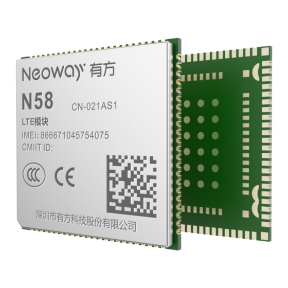
Chapter 2 About N58 2 About N58 N58 is a 4G industrial-grade module developed based on UNISOC UIS8910DM platform, with external dimensions of (30.00± 0.10) mm × (28.00± 0.10) mm × (2.50± 0.15) mm. The module provides connectivity on GSM, FDD-LTE (Cat 1) and TDD-LTE (Cat 1) networks. It provides various hardware... -
Page 14: Block Diagram
FDD-LTE: B1, B3, B5, B8 CA-F1 India Cat 1 TDD-LTE: B40, B41 Supported Supported GSM/GPRS: 900/1800 MHz 2.2 Block Diagram N58 series modules include the following functional units: Baseband chip ⚫ 26 MHz crystal ⚫ Power management ⚫ RF functional ⚫... -
Page 15: Basic Features
Operating: -30° C to +75° C Temperature ranges Extended: -40° C to +85° C Storage: -40° C to +90° C Operating voltage (DC) VBAT: 3.4 V to 4.2 V, typical value: 3.8 V Copyright © Neoway Technology Co., Ltd. All rights reserved. - Page 16 : means the current drawn by the module when there are on-going data services. In this mode, only the current value in LTE system is exemplified. For other current values in other network modes, please refer to the current test report. Copyright © Neoway Technology Co., Ltd. All rights reserved.
- Page 17 One I2C interface, for master mode only. 3GPP Release 13 AT command Neoway extended AT commands PDU, TXT Data PPP, RNDIS, ECM Protocol TCP, UDP, MQTT, FTP, HTTP/HTTPS, SSL, TLS Certification approval CCC, SRRC, RoHS, CE, CTA Copyright © Neoway Technology Co., Ltd. All rights reserved.
-
Page 18: Refference Standards
3GPP TS 27.007 V13.0.0 AT command set for User Equipment (UE) ⚫ 3GPP TS 27.005 V13.0.0 Use of Data Terminal Equipment – Data Circuit terminating Equipment ⚫ (DTE - DCE) interface for Short Message Service (SMS) and Cell Broadcast Service (CBS) Copyright © Shenzhen Neoway Technology Co., Ltd. -
Page 19: Pin Definitions
Chapter 4 Pin Definitions 4 Pin Definitions N58 series modules are equipped with 192 pads, which are introduced in LGA (100 pins) + LCC (92 pins) package. Available functional interfaces include: Power supply, USB, USIM, UART, ADC, I2C, SDIO, etc. -
Page 20: Pin Description
=0V - 0.1V DD_P1 DD_P1 =0.7V DD_P3 DD_P3 P3: 1.8 V =0V - 0.3V DD_P3 GPIO : 1.7 V - 1.9 V (typical value: 1.8 V) =0.8V DD_P3 DD_P3 DD_P3 =0V - 0.2V DD_P3 Copyright © Shenzhen Neoway Technology Co., Ltd. -
Page 21: Table 4-2 Pin Description
Software version (Standard): For data transmission. UART1_RXD UART data input Software version (Open): For data transmission. UART1_CTS UART clear to send Note: UART1_CTS (pin #71) can be used to capture CP log. UART1_RTS UART ready to send Copyright © Shenzhen Neoway Technology Co., Ltd. - Page 22 USIM2 interface USIM2_VCC USIM2 power output This pin is pulled up to USIM2_VCC via a 4.7 kΩ USIM2 data input and USIM2_DATA output resistor. USIM2_CLK USIM2 clock output USIM2_RESET USIM2 reset Copyright © Shenzhen Neoway Technology Co., Ltd.
- Page 23 Leave this pin open if unused. LCD_SPI_CLK SPI clock signal 1.8 V/3.0 V Leave this pin open if unused. Data or command control LCD_SPI_SDC 1.8 V/3.0 V Leave this pin open if unused. signal Copyright © Shenzhen Neoway Technology Co., Ltd.
- Page 24 Leave this pin open if unused. Camera analog power This analog power is disabled by default. If AVDD_CAM 1.6 V - 3.2 V supply enabled, the default output is 1.8 V / 100 mA. Copyright © Shenzhen Neoway Technology Co., Ltd.
- Page 25 Leave this pin open if unused. output of master device Chip selection signal of SPI_CS_N Leave this pin open if unused. slave device GPIO interface GPIO_0 GPIO Leave this pin open if unused. Copyright © Shenzhen Neoway Technology Co., Ltd.
- Page 26 2.8 V - 3.2 V, typical VRTC RTC power supply backup power supply for RTC. value 3.0 V Leave this pin open if unused. Incoming call & SMS RING Leave this pin open if unused. indicator control Copyright © Shenzhen Neoway Technology Co., Ltd.
- Page 27 Chapter 4 Pin Definitions NET_LIGHT Network indication control Leave this pin open if unused. Timing precision is less than 30 ns. 1PPS GNSS timing output This function is only for the N58 module with GNSS. Keypad interface KEYOUT3 Key output KEYOUT2 Key output...
- Page 28 N58 module versions with GNSS: ⚫ The pins #9 and #10 of the module are RESERVED pins and leave these pins open if unused. Pin #89 is a 1PPS pin. See section 5.6.9 “1PPS” for details. Copyright © Shenzhen Neoway Technology Co., Ltd.
-
Page 29: Application Interfaces
Chapter 5 Application Interfaces 5 Application Interfaces N58 provides interfaces for control, communications, peripherals, audio, display, RF and other functions to meet the requirements of different product application scenarios. This chapter describes how to design each interface and provides reference designs and guidelines. -
Page 30: Figure 5-1 Voltage Drop Of The Power Supply
Note that, if there is an instantaneous high current, the above characteristics will lead to unstable operating voltage of the module, and even damage the module. The power supply design of the N58 module depends on the input voltage of power supply. There are three power input types: 3.4 V - 4.2 V power input (typical value: 3.8 V, provided by a battery) -
Page 31: Figure 5-3 Recommended Power Supply Design 2
(220 μF or 100 μF) or an aluminum electrolytic capacitor (470 μF or 1000 μF) at C3 to improve the instantaneous large freewheeling current of the power supply, and its withstand voltage value should be larger than 2 times the power supply voltage. Copyright © Shenzhen Neoway Technology Co., Ltd. -
Page 32: Figure 5-4 Recommended Power Supply Design 3
Keep low ESR bypass capacitors (C3, C5, C6, C7) as close to the module as possible to filter ⚫ out high-frequency interference in the power supply. The design recommendations for the 5.5 V - 24 V power input are as follows: Copyright © Shenzhen Neoway Technology Co., Ltd. -
Page 33: Figure 5-5 Recommended Power Supply Design 4
PCB traces. Place bypass capacitors as close as possible to the power supply interface of the module to filter ⚫ out high-frequency noise signals in the power supply. Copyright © Shenzhen Neoway Technology Co., Ltd. -
Page 34: Vdd_1P8
Leave this pin open if unused. 5.2.1 RESET_N N58 can be reset with the RESET_N pin. When the module is in power-on mode, inputting a negative pulse for more than 50 ms to RESET_N can reset the module. The RESET_N pin is pulled up through a 20 kΩ... -
Page 35: Figure 5-6 Reference Design Of Push-Button Reset
Figure 5-7 Reference reset circuit in which a triode is used for isolation VBAT 20kΩ RESET_N _ ON USER 4.7kΩ N58 Module 47kΩ N58 module reset process is shown in the following figure. Copyright © Shenzhen Neoway Technology Co., Ltd. -
Page 36: Pwrkey_N
Active UART 5.2.2 PWRKEY_N Turning on the N58 module can be done in three different ways, which can be selected according to specific application scenarios. If necessary, please contact Neoway for confirmation. N58 allows startup by the following methods: Figure 5-9 shows the reference design of push-button startup ⚫... -
Page 37: Figure 5-10 Reference Design Of Mcu-Control Startup
470 Ω resistor is recommended) since there is already an internal 1 kΩ series resistor. Otherwise, the module cannot be switched on since the PWRKEY_N is at a high level all the time. Copyright © Shenzhen Neoway Technology Co., Ltd. -
Page 38: Figure 5-12 Power-On Process
When the module is in power-on mode, to turn off the module, the PWRKEY_N pin must be asserted low for greater than 2s and then released. The following figure shows the hardware shutdown process: Copyright © Shenzhen Neoway Technology Co., Ltd. -
Page 39: Sleep
N58 Hardware User Guide Chapter 5 Application Interfaces Figure 5-13 Hardware shutdown process of N58 VBAT T>2s PWRKEY_N Active Inactive UART module shut down software command. Please refer Neoway_N58_AT_Commands_Manual for details. 5.2.3 SLEEP The SLEEP pin is used to control sleep mode of the module and needs to be used together with the AT command. -
Page 40: Figure 5-14 Process Of Entering Into Sleep Mode
Enable UART and process outgoing service process services Complete service Wait till services Complete service Wait till service is procesing? are processed processing? processed MCU pulls SLEEP pin to MCU pulls SLEEP pin Copyright © Shenzhen Neoway Technology Co., Ltd. -
Page 41: Figure 5-16 Process Of Waking Up The Module
Enter/exit sleep mode (send "AT+ENPWRSAVE=2" command to the serial interface of the module to enable sleep and wake-up function of the module.) Enter into sleep mode: keep USER_CTR low ⚫ Exit from sleep mode: keep USER_CTR high ⚫ Copyright © Shenzhen Neoway Technology Co., Ltd. -
Page 42: Peripheral Interfaces
N58 Module 5.3 Peripheral Interfaces N58 provides a variety of peripheral interfaces. In all reference designs in this section, the I/O direction indicated by the module peripheral interface pin name is based on the module, while the peripheral pin naming is based on the peripheral component itself. -
Page 43: Figure 5-18 Recommended Design Of The Usb Interface
USB ID pin Leave this pin open if unused. N58 can implement program download, data communications, and debugging through the USB interface. Only slave mode is supported for USB of the module, which can be used as required. The recommended USB connection circuit is shown in Figure 5-18. -
Page 44: Uart
For module debugging only. UART3_TXD UART data output N58 provides three UART interfaces, two of which support hardware flow control. They support 1.8 V level and baud rates up to 921600 bps. The following figure shows recommended design of the interface. -
Page 45: Figure 5-20 Recommended Voltage-Level Translation Circuit 1
If the UART baud rate is not greater than 115200 bps, it is recommended to design the voltage- level translation solution by referring to the recommended voltage-level translation circuit 2 as shown in Figure 5-21. Copyright © Shenzhen Neoway Technology Co., Ltd. -
Page 46: Figure 5-21 Recommended Voltage-Level Translation Circuit 2
It is recommended to reserve the acceleration capacitor, which can adjust the delay of the − voltage-level translation circuit in some cases. Single-triode voltage-level translation circuit ⚫ For the CTS/RTS pin, it is recommended to design the voltage-level translation solution by referring to Figure 5-22. Copyright © Shenzhen Neoway Technology Co., Ltd. -
Page 47: Usim
Function description Remarks Both 1.8 V and 3 V SIM types are supported: activation and deactivation USIM1_VCC USIM1 power output with an automatic voltage switch from 1.8 V to 3 V is implemented. Copyright © Shenzhen Neoway Technology Co., Ltd. -
Page 48: Figure 5-23 Reference Design Of The Usim Interface (Normally Close Connector)
USIM2_DET USIM2 detection N58 provides two USIM card interfaces, which support dual-SIM single-standby, and the card 1 takes precedence by default. Both 1.8 V and 3.0 V SIM types are supported: activation and deactivation with an automatic voltage switch from 1.8 V to 3.0 V is implemented. The reference schematic diagram of the USIM card interface is shown in Figure 5-23 and Figure 5-24. -
Page 49: Figure 5-24 Reference Design Of Usim Card Interface (Normally Open Connector)
⚫ capacitance value should be not more than 10 pF. They can be unmounted by default. N58 supports USIM card detection, and USIM_DET is a 1.8 V interrupt pin. The USIM detection ⚫ circuit works by checking the level of the voltage across the USIM_DET pin before and after a USIM card is inserted. -
Page 50: Sdio
SDC_DATA_0 SD card SDIO bus data 0 - SDC_DATA_1 SD card SDIO bus data 1 - SDC_DET SD card insertion detect VDD_SDCPULL SD card SDIO bus pull- It shall not supply power to Copyright © Shenzhen Neoway Technology Co., Ltd. -
Page 51: Figure 5-26 Reference Design Of The Sdio Interface
SDC_DET pin after an SD card is installed in the card connector. According to the structure of the card connector, the effective voltage level of insertion detection can be set as high level or low level by software. PCB Design Guidelines Copyright © Shenzhen Neoway Technology Co., Ltd. -
Page 52: Spi
MISO SPI_MISO SPI_MOSI MOSI SPI_CS_N SPI_CLK N58 Module Device (Master) (Slave) 5.3.6 I2C Function Signal Pin SN Remarks description This pin is pulled up to VDD_1P8 via a 1.8 kΩ I2C_SDA I2C data Copyright © Shenzhen Neoway Technology Co., Ltd. -
Page 53: Audio Interfaces
I2C_SCL I2C clock resistor. N58 provides one 1.8 V I2C interface, supporting only master mode and speed rates up to 3.4 Mbps. Figure 5-28 shows the reference design of the I2C interface. Figure 5-28 Reference design of I2C interface VDD_1P8 1.8kΩ... -
Page 54: Analog Audio Output Interfaces
⚫ 5.4.2 Analog Audio Output Interfaces Signal Pin SN Function description Remarks SPK_P Speaker output + Only differential output is supported, with internal Class AB or Class D power SPK_N Speaker output - Copyright © Shenzhen Neoway Technology Co., Ltd. -
Page 55: Figure 5-30 Reference Design Of Audio Interface With Internal Power Amplifier
Class D: 800 mW @ 4.2 V, with a 8 Ω load. N58 can be designed with internal power amplifier or external power amplifier, and the recommended reference designs are as follows: Reference Design of Audio interface with Internal Power Amplifier... -
Page 56: Figure 5-31 Reference Design Of Audio Interface With External Power Amplifier
Isolate the traces from digital signals and clocks as well as other analog signal traces. No signal trace crossing is allowed. Provide enough ground vias and ground reference plane for protection. Copyright © Shenzhen Neoway Technology Co., Ltd. -
Page 57: Video Interfaces
Chapter 5 Application Interfaces 5.5 Video Interfaces 5.5.1 LCD N58 provides an LCD-dedicated SPI interface, supporting frame rates up to QVGA @ 30fps for LCD display. The following shows the LCD interface pin description. Table 5-1 LCD interface description Signal... -
Page 58: Other Functional Interfaces
Network indication control NET_LIGHT is the indication pin of module network status. It can output PWM waveforms with different duty cycles according to different operating states during module operation, and drive LED indicators Copyright © Shenzhen Neoway Technology Co., Ltd. -
Page 59: Ring
RING pin outputs high-level pulses with a pulse width of 600 ms in a period of 5 seconds. After the call is answered, the pin restores to low level, as shown in the following figure. Copyright © Shenzhen Neoway Technology Co., Ltd. -
Page 60: Usb_Boot
USB_BOOT Emergency download pin N58 provides a USB_BOOT pin, which is used to enter the emergency download mode. After the USB_BOOT pin is pulled up to VDD_1P8 before the module is powered up, the module can enter the emergency download mode when it is powered on. This method is used as an emergency solution for product startup failure or malfunction. -
Page 61: Vbackup And Vrtc
RTC. It can supply power in a short time after the VBAT is disconnected to keep the RTC working. The power supply voltage ranges from 2.8 V to 3.2 V and the typical voltage is 3.0 V. The following shows the reference design of the VRTC power supply. Copyright © Shenzhen Neoway Technology Co., Ltd. -
Page 62: Gpio
N58 provides three GPIO interfaces, all with the interrupt function. 5.6.7 GNSS_LNA_EN Signal Pin SN Function description Remarks GNSS_LNA_EN GNSS LNA enabling Leave this pin open if unused. N58 provides an enabling control pin for an external GNSS low-noise amplifier. Copyright © Shenzhen Neoway Technology Co., Ltd. -
Page 63: Keypad
N58 Hardware User Guide Chapter 5 Application Interfaces 5.6.8 Keypad N58 supports a 4x3 matrix keypad. The following shows the pin definitions. Signal Pin SN Function description Remarks KEYOUT3 Key output Leave this pin open if unused. KEYOUT2 Key output Leave this pin open if unused. -
Page 64: 1Pps
1PPS output waveform is shown in Figure 5-38. Figure 5-38 Schematic diagram of 1PPS output waveform For the N58 module versions without GNSS, the 1PPS pin can be used as ADC pin. The detectable voltage range is 0.1 V - VBAT with a 12-bit ADC precision. -
Page 65: Figure 5-39 L-Type Rf Matching Schematics
Figure 5-41 π-type RF matching schematics ANT_MAIN N58 Module Schematic Design Guidelines Element components in the above figures are capacitors, inductors, and 0 Ω resistors. Place ⚫ these RLC components as close to the antenna interface as possible. Copyright © Shenzhen Neoway Technology Co., Ltd. -
Page 66: Ant_Gnss Interface
5.7.2 ANT_GNSS Interface GNSS Impedance Control ANT_GNSS (pin #92) is the GNSS RF interface of the module, which requires a characteristic impedance of 50 Ω. The following shows the GNSS structure inside the module. Copyright © Shenzhen Neoway Technology Co., Ltd. -
Page 67: Figure 5-43 Gnss Rf Structure
(Low Noise Amplifier) inside the active antenna and then sent to the ANT_GNSS pin of the module through the feeder and PCB traces. The following figure shows the reference design of the active GNSS antenna. Copyright © Shenzhen Neoway Technology Co., Ltd. -
Page 68: Figure 5-44 Reference Design Of Active Gnss Antenna
Reference design of passive GNSS antenna After the GNSS antenna receives the GNSS satellite signal, it is transmitted to the ANT_GNSS pin of the N58 module through the PCB traces. The following figure shows a reference design of the passive GNSS antenna. -
Page 69: Ant_Bt Interface
The following methods are commonly used to assemble antennas: Reference design for external antennas (GSC RF connector) ⚫ MM9329-2700RA1 from Murata is recommended. The following figure shows its encapsulation specifications. Copyright © Shenzhen Neoway Technology Co., Ltd. -
Page 70: Figure 5-46 Murata Rf Connector Encapsulation Specifications
Therefore, this connection method is recommended only for 2.4 GHz Wi-Fi or BT/ BLE antennas. The following figure shows the layout of the 2.4 GHz ceramic chip antenna. SLDA52-2R540G-S1TF is used as an example. Copyright © Shenzhen Neoway Technology Co., Ltd. -
Page 71: Figure 5-48 Antenna Layout
Figure 5-49 shows the "No Dround Area" between the antenna and ground that is marked as "5" in Figure 5-48. Figure 5-49 Clearance area (No Ground Area) around the antenna on the PCB board For more details, please refer to the antenna manual and instruction documentation. Copyright © Shenzhen Neoway Technology Co., Ltd. -
Page 72: Electrical Characteristics And Reliability
TDD-LTE: B34, B38, B39, B40, B41 < 3 mA < 16 mA < 340 mA GSM900/850 < 3 mA < 15 mA < 170 mA GSM1800/1900 < 3 mA < 15 mA < 170 mA Copyright © Shenzhen Neoway Technology Co., Ltd. -
Page 73: Temperature Characteristics
± 8 kV ± 15 kV ± 8 kV ± 15 kV Shielding cover ± 8 kV ± 15 kV The above test data are obtained from the test using a N58_Mini_EVB of Neoway. Copyright © Shenzhen Neoway Technology Co., Ltd. -
Page 74: Rf Characteristics
N58 Hardware User Guide Chapter 7 RF Characteristics 7 RF Characteristics N58 provides data connectivity on GSM, FDD-LTE (Cat 1), TDD-LTE (Cat 1) networks. It supports Wi- Fi positioning, BT/BLE wireless connection, and optional GNSS. This chapter introduces the RF characteristics of N58. -
Page 75: Tx Power And Rx Sensitivity
Table 7-3 RX sensitivity Frequency band RX sensitivity ≤ -108 dBm GSM850 ≤ -108 dBm EGSM900 ≤ -108 dBm DCS1800 ≤ -108 dBm PCS1900 ≤ -97 dBm FDD-LTE B1 FDD-LTE B2 < -97 dBm Copyright © Shenzhen Neoway Technology Co., Ltd. -
Page 76: Gnss Technical Parameters
Tracking sensitivity -160 dBm Acquisition sensitivity -154 dBm Positioning accuracy (open space) < 3 m (CEP50) ≤ 1s Hot start (open space) Cold start (open space) < 33s Update frequency < 10 Hz Copyright © Shenzhen Neoway Technology Co., Ltd. -
Page 77: Wlan/Bt Characteristics
Transmitting rate Transmitting power Receiving sensitivity 802.11b (2.4G) 1/2/5.5/11 Mbps -88 dBm 3.2 dBm -88 dBm 2HD5 1 dBm -88 dBm Bluetooth 3DH5 1 dBm -80 dBm BLE/1 Mbps 2 dBm -94 dBm Copyright © Shenzhen Neoway Technology Co., Ltd. -
Page 78: Mechanical Characteristics
N58 Hardware User Guide Chapter 8 Mechanical Characteristics 8 Mechanical Characteristics This chapter introduces mechanical characteristics of N58. 8.1 Dimensions Figure 8-1 Top and side view dimensions (unit: mm) Copyright © Shenzhen Neoway Technology Co., Ltd. -
Page 79: Labeling
N58 module labels are laser-engraved and can withstand high temperatures of up to 260°C. There are two types of the N58 labels: the label with CMIIT ID is applicable to China, and the label without CMIIT ID is applicable to countries or regions outside China. -
Page 80: Reel
N58 Hardware User Guide Chapter 8 Mechanical Characteristics processing methods to ensure the dryness of the product and prolong its service life. 8.3.1 Reel Neoway modules are delivered as reeled tapes as shown below: N58 module Tape Dimensions ITEM 44.0 28.7... -
Page 81: Moisture Sensitivity Level
The baking conditions depend on the moisture degree. It is recommended to bake the module at temperatures higher than 120 degrees for more than 12 hours. Do not bake Neoway modules while contained in a tape and rolled up in reels. For baking, place modules individually onto the oven tray. -
Page 82: Mounting N58 Onto Application Board
N58 Hardware User Guide Chapter 9 Mounting N58 onto Application Board 9 Mounting N58 onto Application Board This chapter describes the package of N58, the recommended footprint of the application PCB, and SMT specifications. 9.1 N58 PCB Package Figure 9-1 Bottom view of N58 PCB package (unit: mm) -
Page 83: Application Pcb Package
9.2 Application PCB Package N58 is equipped with 192 pads which are introduced in 100-pin LCC + 92-pin LGA package. Only GND via-holes and copper pouring are allowed in the shaded area " ” of the PCB package to ensure ⚫... -
Page 84: Stencil
45 seconds and the peak temperature does not exceed 240°C. 9.5 Oven Temperature Profile Neoway will not provide warranties for temperature-sensitive element abnormalities caused by improper temperature control. Thin or long PCB might bend during SMT. So, use loading tools during the SMT and reflow soldering process to avoid poor solder joint caused by PCB bending. -
Page 85: Figure 9-3 Oven Temperature Profile
N58 Hardware User Guide Chapter 9 Mounting N58 onto Application Board Figure 9-3 Oven temperature profile Technical parameters: Ramp up rate: 1 to 4°C/sec ⚫ Ramp down rate: -3 to -1°C/sec ⚫ Soaking zone: 150 - 180°C, Time: 60 - 100s ⚫... -
Page 86: Abbreviations
Digital Output DPSK Differential Phase Shift Keying DQPSK Differential Quadrature Phase Shift Keying Discontinuous Reception Data Terminal Ready Ethernet Control Model eDRX Extended DRX EGSM Enhanced GSM Electronic Static Discharge Equivalent Series Resistance Copyright © Shenzhen Neoway Technology Co., Ltd. - Page 87 Microcontroller Unit Microphone Printed Circuit Board Personal Communications Service Pulse Width Modulation QVGA Quarter Video Graphics Array Random Access Memory Radio Frequency Read-only Memory Real Time Clock Secure Digital SDIO Secure Digital Input Output Copyright © Shenzhen Neoway Technology Co., Ltd.
- Page 88 Universal Serial Bus USIM Universal Subscriber Identity Module VBAT Battery Voltage VSWR Voltage Standing Wave Ratio Wi-Fi Wireless Fidelity WCDMA Wide-band Code Division Multiple Access Wireless Coexistence Interface WLAN Wireless Local Area Network Copyright © Shenzhen Neoway Technology Co., Ltd.
Need help?
Do you have a question about the N58 and is the answer not in the manual?
Questions and answers