Neoway N58 Hardware User's Manual
Hide thumbs
Also See for N58:
- Hardware user's manual (88 pages) ,
- Hardware user's manual (74 pages) ,
- Hardware user's manual (45 pages)
Table of Contents
Advertisement
Quick Links
Advertisement
Table of Contents

Related Manuals for Neoway N58


Summary of Contents for Neoway N58
- Page 1 Hardware User Guide Issue 2.5 Date 2021-10-29...
- Page 2 THIS GUIDE PROVIDES INSTRUCTIONS FOR CUSTOMERS TO DESIGN THEIR APPLICATIONS. PLEASE FOLLOW THE RULES AND PARAMETERS IN THIS GUIDE TO DESIGN AND COMMISSION. NEOWAY WILL NOT TAKE ANY RESPONSIBILITY OF BODILY HURT OR ASSET LOSS CAUSED BY IMPROPER OPERATIONS. THE INFORMATION IN THIS DOCUMENT IS SUBJECT TO CHANGE WITHOUT NOTICE DUE TO PRODUCT VERSION UPDATE OR OTHER REASONS.
-
Page 3: Table Of Contents
5.4.2 Analog Audio Output Interfaces ..................53 5.5 Video Interfaces ......................... 55 5.5.1 LCD ........................... 55 5.5.2 Camera ..........................56 5.6 Other Interfaces ......................... 56 5.6.1 ADC ........................... 56 5.6.2 NET_LIGHT ........................56 Copyright © Neoway Technology Co., Ltd. All rights reserved. - Page 4 9.1 Module PCB Package ........................ 81 9.2 Application PCB Package ......................82 9.3 Stencil ............................82 9.4 Solder Paste ..........................83 9.5 SMT Furnace Temperature Curve ....................83 Abbreviations ..................85 Copyright © Neoway Technology Co., Ltd. All rights reserved.
- Page 5 Figures Figures Figure 2-1 Block diagram ......................... 14 Figure 4-1 Pin layout of the N58 module (top view) ................. 18 Figure 5-1 Voltage drop of the power supply ................... 29 Figure 5-2 Recommended design 1 ....................29 Figure 5-3 Recommended design 2 ....................30 Figure 5-4 Recommended design 3 ....................
- Page 6 Figure 8-2 N58 label examples ......................78 Figure 9-1 Bottom view of the N58 module PCB package (unit: mm) ..........81 Figure 9-2 Top view of the recommended N58 application PCB package (unit: mm) ..... 82 Figure 9-3 SMT furnace temperature curve ..................83...
- Page 7 Table 5-2 Description of camera function pins ................. 56 Table 6-1 Electrical characteristics of the N58 module ..............71 Table 6-2 Current consumption of the N58 module (typical) ............71 Table 6-3 ESD protection characteristics ..................72 Table 7-1 Operating bands of the N58 module ................73 Table 7-2 RF TX power of the N58 module ..................
-
Page 8: About This Document
About This Document Scope This document is applicable to the N58 series. It describes N58 information and functional interface characteristics, and provides a reference design for each functional interface. The reference design in this document is for reference only, and user applications must be designed according to actual scenarios and conditions. - Page 9 2021-09 Added chapter 3 "Reference Standards" to describe Wu Yongqiang the reference standards of the N58 module design. Added the VCC_GNSS_BIAS pin description of the N58 module with the GNSS function. Updated the N58 module startup, shutdown, and ...
-
Page 10: Conventions
If these points are not followed, the module or user device may fail. Indicates instructions or tips. This symbol provides advices or suggestions that may be useful when using the module. Copyright © Neoway Technology Co., Ltd. All rights reserved. -
Page 11: Related Documents
N58 Hardware User Guide About This Document Related Documents Neoway_N58_Datasheet Neoway_N58_Product_Specifications Neoway_N58_AT_Command_Mannual Neoway_N58_EVK_User_Guide Copyright © Neoway Technology Co., Ltd. All rights reserved. -
Page 12: Safety Recommendations
Follow the requirements below during the application design and use of this product: Do not disassemble this product without permission from Neoway. Otherwise, we are entitled to refuse to provide further warranty. Design your application correctly based on the hardware user guide. Connect this product to a stable power supply and route traces following fire safety standards. -
Page 13: About N58
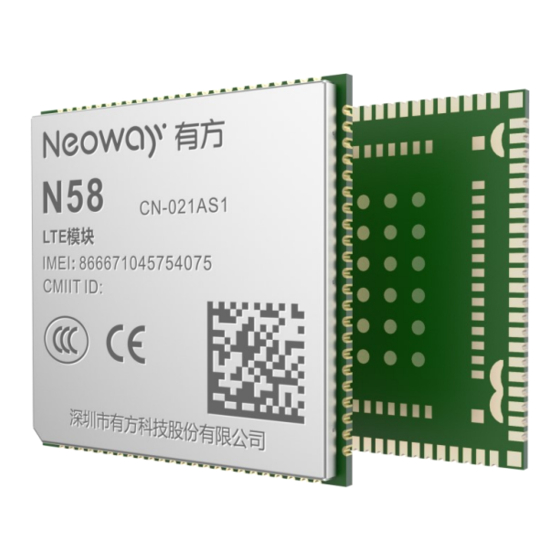
Chapter 2 About N58 2 About N58 N58 is an industrial LTE module that is developed based on the UNISOC UIS8910DM platform. Its dimensions are (30.00± 0.15) mm × (28.00± 0.15) mm × (2.60± 0.20) mm. This module supports GSM, FDD-LTE (Cat 1), and TDD-LTE (Cat 1) network modes. -
Page 14: Block Diagram
ANT_GNSS GNSS RF front-end VBAT PWRKEY_N RESET Power manager RF transceiver MIC, SPK Baseband 26 MHz crystal NOR flash (64 Mb) + PSRAM (128 Mb) Digital interface KEYP USIM SDIO UART Copyright © Neoway Technology Co., Ltd. All rights reserved. -
Page 15: Basic Features
Matrix keyboard interfaces with 3 rows and 4 columns. One 12-bit ADC interface, voltage detection range: 0.1 V to VBAT. One SDIO interface, used for an SD card. One 1PPS interface. Copyright © Neoway Technology Co., Ltd. All rights reserved. - Page 16 In operating mode , only an example of the current in LTE mode is provided. For details about the current in non- LTE modes, see the N58 current test report. Copyright © Neoway Technology Co., Ltd. All rights reserved.
-
Page 17: Reference Standards
N58 Hardware User Guide Chapter 3 Reference Standards 3 Reference Standards The N58 module design references the following standards: 3GPP TS 36.521-1 V13.0.0 User Equipment (UE) conformance specification; Radio transmission and reception; Part 1: Conformance Testing 3GPP TS 21.111 V13.0.0 USIM and IC card requirements ... -
Page 18: Module Pins
Chapter 4 Module Pins 4 Module Pins The N58 module has 192 pins and uses the LGA (100 pins)+LCC (92 pins) package. It supports the functional interfaces, including the power, USB, USIM, UART, ADC, I2C, and SDIO interfaces. 4.1 Pin Layout Figure 4-1 shows the pin layout of the N58 module. -
Page 19: Pin Description
= 4.2 V current to VBAT. module Used only for level 1.8 V power = 1.8 V norm VDD_1P8 shifting. Leave this pin output = 50 mA floating if it is not used. Copyright © Neoway Technology Co., Ltd. All rights reserved. - Page 20 CP-side UART1_RTS the user to logs of the module. send data UART2 interface Data Software (standard) UART2_TXD sending version: These pins Data used UART2_RXD receiving command communications. UART2_CTS User Copyright © Neoway Technology Co., Ltd. All rights reserved.
- Page 21 Connect this pin to USIM2 data USIM2_VCC by using USIM2_DATA kΩ pull-up input/output resistor. USIM2 clock USIM2_CLK output USIM2_RESET USIM2 reset USIM2 If the hot plug function USIM2_DET detection is not used, refer to Copyright © Neoway Technology Co., Ltd. All rights reserved.
- Page 22 Leave this pin floating LCD_SPI_CLK 1.8 V/3.0 V signal if it is not used. Data command Leave this pin floating LCD_SPI_SDC 1.8 V/3.0 V control if it is not used. signal Copyright © Neoway Technology Co., Ltd. All rights reserved.
- Page 23 Leave this pin floating input if it is not used. clock Leave this pin floating CAM_SPI_CLK signal if it is not used. Leave this pin floating CAM_I2C_SDA I2C data if it is not used. Copyright © Neoway Technology Co., Ltd. All rights reserved.
- Page 24 The power supply is Pull-up enabled default, power VDD_SDCPUL and the output is 3.1 supply 1.6 V to 3.2 V V/150 the SD card forbidden supply data bus power to other loads. Copyright © Neoway Technology Co., Ltd. All rights reserved.
- Page 25 Leave this pin floating GPIO_3 GPIO if it is not used. Audio SPK interface Speaker SPK_P output positive Speaker SPK_N output negative Audio MIC interface Microphone MIC_P input positive Microphone MIC_N input negative Copyright © Neoway Technology Co., Ltd. All rights reserved.
- Page 26 N58 module with GNSS have this function. GNSS active Only the sub-models antenna VCC_GNSS_BI of the N58 module with PO/DO power GNSS have this supply function. detection Keypad interface Copyright © Neoway Technology Co., Ltd. All rights reserved.
- Page 27 Pin 9 and pin 10 of the N58 module can be used for the UART4 interface (pin 9 is used for UART4_TXD, pin 10 is used for UART4_RXD, and the interface level is 1.8 V). Pin 89 of the N58 module can be used for the ADC2 interface (ADC2 interface characteristics are the same as ADC1 interface characteristics ).
-
Page 28: Application Interfaces
Chapter 5 Application Interfaces 5 Application Interfaces N58 provides the control, communications, peripheral, audio, display, and RF interfaces to meet the product functional requirements in different application scenarios. This chapter describes how to design each interface and provides reference designs and guidelines. -
Page 29: Figure 5-1 Voltage Drop Of The Power Supply
The power supply design of the N58 module is determined by the power input voltage. The designs are classified by power input voltage as follows: ... -
Page 30: Figure 5-3 Recommended Design 2
Place low-ESR bypass capacitors (C4, C5, C6, and C7) close to the module to filter out high- frequency interference from the power supply. The recommended 4.2 V–5.5 V input design is as follows. Copyright © Neoway Technology Co., Ltd. All rights reserved. -
Page 31: Figure 5-4 Recommended Design 3
0.1uF (5.5V-24V) BOOST VBAT 3.3uH 100uF 22uF 0.1uF 470uF 100uF 22uF 0.1uF 100pF 33pF PWR_EN SS36 1kΩ C8 C9 C10 C11 C12 RT/CLK 47.5kΩ 47.5KΩ P-PAD COMP 12KΩ 12kΩ 100pF 0.01uF Copyright © Neoway Technology Co., Ltd. All rights reserved. - Page 32 FB pin and COMP pin as possible. The GND pin and bottom pad of the chip must be grounded to ensure good heat dissipation and noise isolation. Copyright © Neoway Technology Co., Ltd. All rights reserved.
-
Page 33: Vdd_1P8
5.2.1 PWRKEY_N There are three startup control methods for the N58 module. You can choose to use a method based on a specific application scenario. If necessary, contact Neoway FAE for confirmation. The N58 module allows startup by the following controls: ... -
Page 34: Figure 5-6 Reference Design Of Module Startup Controlled By Button
Figure 5-6 Reference design of module startup controlled by button VBAT 20kΩ PWRKEY_N 1kΩ Main Chip 470Ω N58 Module Figure 5-7 Reference design of module startup controlled by MCU VBAT 20kΩ PWRKEY_N 1kΩ Main Chip 4.7kΩ USER_ON 47kΩ N58 Module Copyright © Neoway Technology Co., Ltd. All rights reserved. -
Page 35: Figure 5-8 Reference Design Of Automatic Startup Once Powered On
Therefore, do not perform other operations on the module until it is initialized completely. The following figure shows the startup process. Copyright © Neoway Technology Co., Ltd. All rights reserved. -
Page 36: Figure 5-9 Startup Process
2s at the PWRKEY_N pin can trigger power-off of the module. The following figure shows the hard shutdown process. Figure 5-10 Hard shutdown process VBAT T>2s PWRKEY_N Active Inactive UART Copyright © Neoway Technology Co., Ltd. All rights reserved. -
Page 37: Reset_N
Neoway_N58_AT_Command_Manual. 5.2.2 RESET_N The RESET_N pin is used to reset the N58 module. When the module is working properly, inputting a low-level pulse for more than 50 ms at the RESET_N pin can trigger the reset process of the module. -
Page 38: Sleep
N58 Hardware User Guide Chapter 5 Application Interfaces The following figure shows the reset process of the N58 module. Figure 5-13 Reset process of the N58 module VBAT T>50ms RESET_N Active Inactive Active UART 5.2.3 SLEEP The SLEEP pin is the control pin of the sleep mode, and it needs to be used together with AT commands. -
Page 39: Figure 5-14 Process Of Entering The Sleep Mode
Enable UART and process outgoing service process services Complete service Wait till services Complete service Wait till service is procesing? are processed processing? processed MCU pulls SLEEP pin to MCU pulls SLEEP pin Copyright © Neoway Technology Co., Ltd. All rights reserved. -
Page 40: Figure 5-16 Process Of Exiting From The Sleep Mode
If a user wants to control the module's SLEEP pin to implement the wake-up function, the reference design of the N58 module sleep and wake-up control circuit is recommended, as shown in Figure 5- Entering the sleep mode/exiting from the sleep mode (AT+ENPWRSAVE=2 can be sent over the UART interface to enable the sleep and wake-up functions.) -
Page 41: Peripheral Interface
4.5 V < USB_VBUS < 5.2 V, typical value: 5 V. detection pin USB_DM AIO USB data minus USB 2.0. These pins are used for software download and data transmission. Route DM USB_DP AIO USB data positive Copyright © Neoway Technology Co., Ltd. All rights reserved. -
Page 42: Figure 5-18 Reference Design Of The Usb Connection Circuit
Leave this pin floating if it is not used. N58 can implement program download, data communications, and debugging by using the USB interface. The module USB supports only the slave mode, and users can choose to use it according to their needs. -
Page 43: Uart
UART3_TXD Data sending The N58 module can provide three UART interfaces, and two of them support hardware flow control. The UART interfaces support 921600 bps at most. The level at the interfaces is 1.8 V. The following figure shows the reference design of UART connections. -
Page 44: Figure 5-19 Reference Design Of Uart Connections
VL is the reference voltage of IO_VL1 and IO_VL2, ranging from 1.5 V to 5.5 V. − VCC is the reference voltage of IO_VCC1 and IO_VCC2, ranging from 1.5 V to 5.5 V. − Copyright © Neoway Technology Co., Ltd. All rights reserved. -
Page 45: Figure 5-21 Recommended Level Shifting Circuit 2
MCU_TXD and MCU_RXD are the sending and receiving interfaces of the MCU, respectively. TXD and RXD are the sending and receiving interfaces of the module, respectively. VCC_IO is the IO voltage of the MCU, and VDD_1P8 is the IO voltage of the module. Copyright © Neoway Technology Co., Ltd. All rights reserved. -
Page 46: Usim
Connect this pin to USIM1_VCC by USIM1_DATA using a 4.7 kΩ pull-up resistor. input/output USIM1_CLK USIM1 clock output USIM1_RESET USIM1 reset USIM1_DET USIM1 detection USIM2_VCC USIM2 power output Adaptive 1.8 V/3V. Copyright © Neoway Technology Co., Ltd. All rights reserved. -
Page 47: Figure 5-23 Reference Design Of Usim Card (With The Hot Plug Function) Interfaces
USIM2_DET USIM2 detection N58 provides two USIM card interfaces and supports dual USIM single standby. USIM1 is used by default. Adaptive 1.8 V/3 V USIM cards are used. Figure 5-23 shows the reference design of USIM card (with the hot plug function) interfaces. -
Page 48: Figure 5-24 Reference Design Of Usim Card (Without The Hot Plug Function) Interfaces
USIM card detected while low level means no USIM card detected. If the user USIM card does not use the hot plug function, the USIM_DET pin of the N58 module must be pulled up to 1.8 V by using a 47 kΩ resistor in series, and the software must disable the USIM hot plug detection function. -
Page 49: Sdio
SDC _ CMD SDC _ DATA 0 DATA0 SDC _ DATA DATA1 SDC _ DATA DATA2 SDC _ DATA DATA3 47 k Ω SDC _ DET N58 Module SD Card Slot Copyright © Neoway Technology Co., Ltd. All rights reserved. -
Page 50: Spi
Chip select signal of the slave SPI_CS_N device The SPI interface supports 1.8 V level and frequency of up to 50 MHz. It supports only the master mode. The following figure shows the reference design. Copyright © Neoway Technology Co., Ltd. All rights reserved. -
Page 51: I2C
I2C clock pull-up resistor. The N58 module provides one I2C interface. The I2C interface supports only the master mode, the maximum rate of the interface is 3.4 Mbps, and the interface level is 1.8 V. Figure 5-27 shows the I2C reference design. -
Page 52: Audio Interfaces
Internal built-in bias voltage. MIC_N MIC input negative N58 supports one differential MIC input, with internal built-in bias voltage. The following figure shows the reference design of differential MIC input. Figure 5-28 Reference design of differential MIC input MIC_ P... -
Page 53: Analog Audio Output Interfaces
D1 and D2 are TVS diodes used to prevent ESD from damaging the module. B1 and B2 are ferrite beads used to filter out high-frequency noise. It is recommended to use ferrite beads specifically for audio. Copyright © Neoway Technology Co., Ltd. All rights reserved. -
Page 54: Figure 5-30 Reference Design Of The External Power Amplifier
N58 Module Schematic design guidelines: Connect the SPK output of the N58 module to the power amplifier with differential connections, and select a power amplifier that can support differential input for the audio power amplifier. Note that the over-current capability of L1 and L2 must meet the current requirements at the maximum power. -
Page 55: Video Interfaces
5.5 Video Interfaces 5.5.1 LCD N58 has an SPI interface dedicated to the LCD function, and supports the highest frame rate of LCD display QVGA@30 fps. The following table provides the description of LCD function pins. Table 5-1 Description of LCD function pins Pin Name Pin No. -
Page 56: Camera
Chapter 5 Application Interfaces 5.5.2 Camera N58 has an SPI interface dedicated to the camera function, and supports the highest frame rate of the camera VGA@15 fps. The following table provides the description of camera function pins. Table 5-2 Description of camera function pins Pin Name Pin No. -
Page 57: Ring
RING pin outputs a high pulse with a pulse width of 600 ms and a period of 5 seconds during the ringing period. After the call is answered, the pin restores to low-level output. The following figure shows the RING indicator for an incoming voice call. Copyright © Neoway Technology Co., Ltd. All rights reserved. -
Page 58: Usb_Boot
Add an ESD component to protect USB_BOOT in a circuit. The following figure shows the reference design of forcible download. Copyright © Neoway Technology Co., Ltd. All rights reserved. -
Page 59: Vbackup And Vrtc
Otherwise, GNSS is cold started every time. VRTC is the backup power pin of N58 module RTC and can be connected to a coin battery or farad capacitor. It can provide short-term power supply to keep the RTC working after the VBAT is disconnected. -
Page 60: Gpio
GPIO, with the interruption function used. Leave this pin floating if it is not GPIO_3 GPIO, with the interruption function used. N58 provides three GPIO interfaces, and all of these GPIO interfaces support the interruption function. 5.6.7 GNSS_LNA_EN Pin Name Pin No. Function Remarks GNSS_LNA_EN GNSS LNA enabling Leave this pin floating if it is not used. -
Page 61: Keypad
N58 Hardware User Guide Chapter 5 Application Interfaces 5.6.8 Keypad N58 supports matrix keyboard (4x3: 4 rows and 3 columns). The following table provides the description of keypad pins. Pin Name Pin No. Function Remarks KEYOUT3 Key output Leave this pin floating if it is not used. -
Page 62: 1Pps
Figure 5-37 1PPS output waveform 100ms T=1s For sub-models of the N58 module without GNSS, the 1PPS pin can be used as the ADC pin. The detectable voltage ranges from 0.1 V to VBAT, and 12-bit precision resolution is supported. 5.6.10 VCC_GNSS_BIAS Pin Name Pin No. -
Page 63: Rf Interfaces
Chapter 5 Application Interfaces Over-current: If the current is greater than or equal to 45 mA or a short circuit occurs, the N58 module indicates that the antenna is in the over-current state. Figure 5-38 shows the reference design of GNSS active antenna power supply and detection circuit. -
Page 64: Figure 5-39 L-Type Matching Network
Add ESD protection if the antenna might generate static electricity. ESD components with ultra- low junction capacitance can be used. It is recommended to use a TVS diode with a junction Copyright © Neoway Technology Co., Ltd. All rights reserved. -
Page 65: Ant_Gnss Interface
5.7.2 ANT_GNSS Interface GNSS Impedance Control ANT_GNSS (92nd pin) is the GNSS RF interface of N58, which requires a characteristic impedance of 50 Ω. The following figure shows the GNSS structure inside the N58 module. Copyright © Neoway Technology Co., Ltd. All rights reserved. -
Page 66: Figure 5-43 Gnss Structure Inside The Module
After the GNSS antenna receives GNSS satellite signals, the LNA amplifies the signals first and then transmits them to the ANT_GNSS pin of N58 through the feeder and PCB traces. The following figure shows the reference design of an active GNSS antenna. -
Page 67: Figure 5-44 Reference Design Of An Active Gnss Antenna
Reference Design of a Passive GNSS Antenna After the GNSS antenna receives GNSS satellite signals, the signals are transmitted to the ANT_GNSS pin of N58 through the PCB traces. The following figure shows the reference design of a passive GNSS antenna. -
Page 68: Ant_Bt Interface
GNSS and affect performance. 5.7.3 ANT_BT Interface The 94th pin of the N58 module is a Bluetooth antenna interface pin. It has a characteristic impedance of 50 Ω. For the schematic design and PCB design of the Bluetooth antenna interface, refer to section 5.7.1 "ANT_MAIN Antenna Interface."... -
Page 69: Figure 5-46 Package Specifications Of Murata's Gsc Rf Connector
PCB antennas or ceramic antennas to cover a wide frequency. The following figure shows the layout of the 2.4 GHz patch ceramic antenna. SLDA52-2R540G- S1TF is used as an example. Copyright © Neoway Technology Co., Ltd. All rights reserved. -
Page 70: Figure 5-48 Antenna Layout Example
5 in Figure 5-48 is the area between the antenna and ground. Figure 5-49 shows the layout of this area. Figure 5-49 Layout around the antenna For details, refer to antenna manufacturers' usage recommendations and documentation. Copyright © Neoway Technology Co., Ltd. All rights reserved. -
Page 71: Electrical Characteristics And Reliability
Chapter 6 Electrical Characteristics and Reliability 6 Electrical Characteristics and Reliability This chapter describes the electrical characteristics and reliability of the N58 module, including the input and output voltage and current of the power supply, the current consumption of the module in different states, the operating and storage temperature ranges, and the ESD protection characteristics. -
Page 72: Temperature Characteristics
Table 6-3 ESD protection characteristics Test Point Contact Discharge Air Discharge ± 8 kV ± 15 kV ± 8 kV ± 15 kV Shielding cover ± 8 kV ± 15 kV Copyright © Neoway Technology Co., Ltd. All rights reserved. -
Page 73: Rf Characteristics
Chapter 7 RF Characteristics 7 RF Characteristics The N58 module supports GSM, FDD-LTE (Cat 1), and TDD-LTE (Cat 1) network modes. It supports Wi-Fi positioning and BT/BLE wireless connectivity, and supports GNSS (optional). This chapter describes the RF characteristics of the N58 module. -
Page 74: Tx Power And Rx Sensitivity
N58 Hardware User Guide Chapter 7 RF Characteristics 7.2 TX Power and RX Sensitivity Table 7-2 RF TX power of the N58 module Band Maximum Power Minimum Power GSM850 33 dBm± 2 dB 5 dBm± 2 dB EGSM900 33 dBm± 2 dB 5 dBm±... -
Page 75: Gnss Parameters
Positioning precision (in an open environment) < 3 m (CEP50) ≤ 1s Hot start time (in an open environment) Cold start time (in an open environment) < 33s Update frequency < 10 Hz Copyright © Neoway Technology Co., Ltd. All rights reserved. -
Page 76: Wlan/Bt Characteristics
TX Power RX Sensitivity 802.11b (2.4G) 1/2/5.5/11 Mbps -88 dBm 3.2 dBm -88 dBm 2HD5 1 dBm -88 dBm Bluetooth 3DH5 1 dBm -80 dBm BLE/1 Mbps 2 dBm -94 dBm Copyright © Neoway Technology Co., Ltd. All rights reserved. -
Page 77: Mechanical Characteristics
N58 Hardware User Guide Chapter 8 Mechanical Characteristics 8 Mechanical Characteristics This chapter describes the mechanical characteristics of the N58 module. 8.1 Dimensions Figure 8-1 N58 top and side dimensions (unit: mm) Copyright © Neoway Technology Co., Ltd. All rights reserved. -
Page 78: Label
The pictures above are only for reference. 8.3 Packaging The N58 module uses a surface-mount method for furnace welding. A moisture-proof packaging method is used to prevent the product from being moist from production to users' use. That is, a processing method, such as using the aluminum foil bag, desiccant, humidity indicator card, tape, or vacuum, is used to ensure the dryness of the product and prolong the lifetime. -
Page 79: Reel And Tape
N58 Hardware User Guide Chapter 8 Mechanical Characteristics 8.3.1 Reel and Tape N58 modules in mass production are delivered in the following packaging. module Tape details ITEM 44.0 28.7 28.70 40.4 1.75 20.2 3.55 36.0 0.30 +0.1 +0.1 +0.1 +0.1 +0.1... -
Page 80: Moisture
Reel details 8.3.2 Moisture N58 is a level-3 moisture sensitive device, in compliance with standard IPC/JEDEC J-STD-020. Pay attention to all the related requirements for using this kind of components. After the module is unpacked, if it is exposed to the air for a long time, the module will be moist, and the module may be damaged during reflow soldering or welding in a lab. -
Page 81: Assembly
N58 Hardware User Guide Chapter 9 Assembly 9 Assembly This chapter describes the N58 module package, the recommended application package, and technical points related to SMT. 9.1 Module PCB Package Figure 9-1 Bottom view of the N58 module PCB package (unit: mm) -
Page 82: Application Pcb Package
Chapter 9 Assembly 9.2 Application PCB Package The N58 module has 192 pins and uses the LGA (100 pins)+LCC (92 pins) package. The recommended PCB package is as follows. To ensure the normal operation of the module, there can be only GND vias and pour copper under the shadow areas "... -
Page 83: Solder Paste
Chapter 9 Assembly 9.4 Solder Paste The solder paste volume and the PCB flatness play key roles in the production yield. Do not use solder pastes with lead that use a module technique that is different from Neoway module technique. ... - Page 84 Then gently remove the module using tweezers. Do not shake the module in high temperatures while removing it. Otherwise, the components inside the module might get misplaced and cannot be repaired. Copyright © Neoway Technology Co., Ltd. All rights reserved.
-
Page 85: Abbreviations
DPSK Differential Phase Shift Keying DQPSK Differential Quadrature Phase Shift Keying Discontinuous Reception Data Terminal Ready Ethernet Control Model eDRX Extended DRX EGSM Enhanced GSM Electronic Static Discharge Equivalent Series Resistance Copyright © Neoway Technology Co., Ltd. All rights reserved. - Page 86 Printed Circuit Board Personal Communications Service Pulse Width Modulation QVGA Quarter Video Graphics Array Random Access Memory Radio Frequency Read-only Memory Real Time Clock Secure Digital SDIO Secure Digital Input Output Copyright © Neoway Technology Co., Ltd. All rights reserved.
- Page 87 Universal Serial Bus USIM Universal Subscriber Identity Module VBAT Battery Voltage VSWR Voltage Standing Wave Ratio Wi-Fi Wireless Fidelity WCDMA Wide-band Code Division Multiple Access Wireless Coexistence Interface WLAN Wireless Local Area Network Copyright © Neoway Technology Co., Ltd. All rights reserved.
Need help?
Do you have a question about the N58 and is the answer not in the manual?
Questions and answers
I want to make one GPIO pin as output pin but i was not able to do that.I want to use 1 macro for the GPIO how to define that.When i use funtion for to set the GPIO pin as output direction it is always failing.Give em solution for this.