Table of Contents
Advertisement
Quick Links
Advertisement
Table of Contents

Related Manuals for Neoway N51


Summary of Contents for Neoway N51
- Page 1 Hardware User Guide Issue 1.0 Date 2018-10-25 Neoway Product Document...
- Page 2 THIS GUIDE PROVIDES INSTRUCTIONS FOR CUSTOMERS TO DESIGN THEIR APPLICATIONS. PLEASE FOLLOW THE RULES AND PARAMETERS IN THIS GUIDE TO DESIGN AND COMMISSION. NEOWAY WILL NOT TAKE ANY RESPONSIBILITY OF BODILY HURT OR ASSET LOSS CAUSED BY IMPROPER OPERATIONS. THE INFORMATION IN THIS DOCUMENT IS SUBJECT TO CHANGE WITHOUT NOTICE DUE TO PRODUCT VERSION UPDATE OR OTHER REASONS.
-
Page 3: Table Of Contents
Hardware User Guide Contents 1 About N51 ....................1 1.1 Product Overview ......................... 1 1.2 Block Diagram ..........................1 1.3 Basic Features ..........................2 2 Module Pins ....................4 2.1 Pad Layout ........................... 4 2.2 Pin Description ..........................5 3 Application Interfaces ................10 3.1 Power Interfaces ........................ - Page 4 6.2 Three Views ..........................42 6.3 Packing ............................42 6.3.1 Tray ............................ 42 6.3.2 Moisture ..........................42 7 Mounting N51 onto the Application Board ..........43 7.1 Bottom Dimensions ........................43 7.2 Application Foot Print ......................... 44 7.3 Stencil ............................44 7.4 Solder Paste ..........................
- Page 5 Hardware User Guide Table of Figures Figure 1-1 Block diagram ........................2 Figure 2-1 Pin assignment of N51 ...................... 4 Figure 3-1 Reference design 1 ......................11 Figure 3-2 Reference design 2 ......................11 Figure 3-3 Reference design 3 ......................12 Figure 3-4 Reference design of startup controlled by button ............
- Page 6 Figure 6-1 N51 dimensions (Unit: mm) .................... 41 Figure 6-2 Three views of N51 ......................42 Figure 7-1 N51 bottom dimensions (Unit: mm) ................43 Figure 7-2 Recommended PCB foot print (Unit: mm) ..............44 Figure 7-3 SMT furnace temperature curve ..................45...
- Page 7 Table 4-3 Temperature features of N51 .................... 38 Table 4-4 N51 ESD protection ......................38 Table 5-1 Operating band of N51 ..................... 39 Table 5-2 TX power and RX sensitivity of N51 ................. 39 Copyright © Neoway Technology Co., Ltd...
- Page 8 Means reader be careful. In this situation, you might perform an action that could result in module or product damages. Means note or tips for readers to use the module Copyright © Neoway Technology Co., Ltd...
- Page 9 Hardware User Guide Related Documents Neoway_N51_Datasheet Neoway_N51_Product_Specifications Neoway_N51_AT_Command_Mannual Neoway_N51_EVK_User_Guide Copyright © Neoway Technology Co., Ltd viii...
-
Page 10: About N51
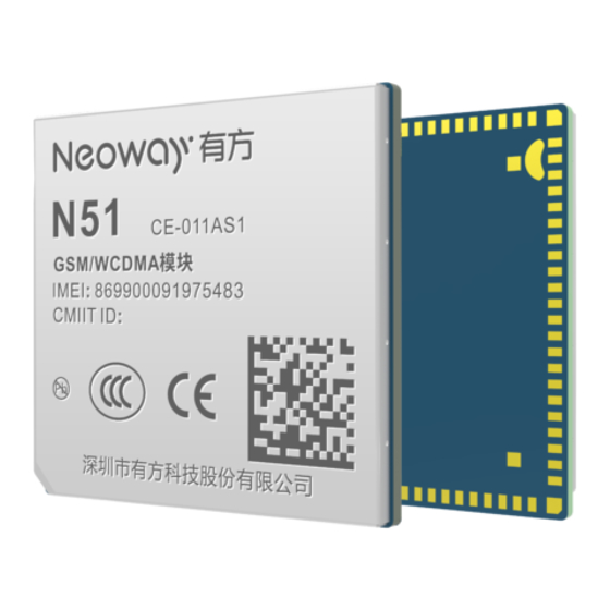
UMTS: B1, B2, B5, B8 GSM/GPRS: 850/900/1800/1900 MHz N51 adopts 100-pin LGA package and its dimensions are 30 mm x 28 mm x 2.35 mm. With industrial- grade performance, this module is well applicable to electrical terminals, industrial control, POS, and other IoT terminals. -
Page 11: Basic Features
Operating: -30° C to 75 ° C Temperature ranges Extended: -40℃ to 85 ° C Storage: -45℃ to +90 ° C Operating voltage VBAT: 3.3 V to 4.3 V, TYP: 3.8 V Current See Table 4-2. Copyright © Neoway Technology Co., Ltd... - Page 12 One 10-bit ADC interface, detectable voltage ranging from 0.1 to 1.7 V. Application Interfaces One SPI interface Four GPIOs with interrupt One I2C interface One set of 3*3 key pads One audio input and one audio output AT commands Protocol Certification approval Copyright © Neoway Technology Co., Ltd...
-
Page 13: Module Pins
Hardware User Guide 2 Module Pins There are 100 pins on N51 and their pads are introduced in LGA package. 2.1 Pad Layout Figure 2-1 shows the pad layout of N51. Figure 2-1 Pin assignment of N51 Copyright © Neoway Technology Co., Ltd... -
Page 14: Pin Description
1.8 V/2.85 V =1.62~1.95 V, =2.57~3.1 V, =0~0.18 V =0 V~0.29 V Table 2-2 Pin Description Level Signal Function Remarks Feature Power Interfaces Main power supply : 3.3~4.3 V, TYP: 3.8 V, VBAT input Copyright © Neoway Technology Co., Ltd... - Page 15 Data transmitting used. Leave this pin floating if it is not UART1_RXD Data receiving used. UART2_TXD Data transmitting Used for data transmission. Leave this pin floating if it is not UART2_RXD Data receiving used. Copyright © Neoway Technology Co., Ltd...
- Page 16 Leave this pin floating if it is not SPI_MISO Master input used. Leave this pin floating if it is not SPI_MOSI Master output used. Leave this pin floating if it is not SPI_CS_N Chip select used. Copyright © Neoway Technology Co., Ltd...
- Page 17 Leave this pin floating if it is not SPK_N SPK output minus used. Antenna Interface Main antenna 50 Ω impedance for traces Other Interface RING Incoming call/SMS P2 Leave this pin floating if it is not Copyright © Neoway Technology Co., Ltd...
- Page 18 Reserved Pins 3, 4, 5, 6, 7, 8, 9, 10, 11, 12, 34, 43, 50, 54, 55, RESERVED 56, 57, 58, 59, 60, 61, 64, 65, 66, 67, 68, 71, 72, 73, 78 Copyright © Neoway Technology Co., Ltd...
-
Page 19: Application Interfaces
The power supply design covers two parts: schematic design and PCB layout.. Schematic Design Design the circuit of the power supply for N51 based on the input voltage you choose. Generally there are two types of input voltages: 3.3V-4.3 V (3.8 V typically, output by battery) ... -
Page 20: Figure 3-1 Reference Design 1
Q100 C105 C106 R100 C107 C108 C109 C110 C111 D101 10 kΩ 10 uF 0.1 uF 470 uF 10 uF 0.1 uF 100 pF 33 pF PWR_EN R101 Q101 4.7 kΩ R102 47 kΩ Copyright © Neoway Technology Co., Ltd... -
Page 21: Figure 3-3 Reference Design 3
Therefore, the back-end components and the module are protected. Place C112 and C113 close to the power supply to filter noise from it. Place C114 to C118 close to the module. Copyright © Neoway Technology Co., Ltd... - Page 22 Never use a diode to make the drop voltage between a higher input and module power. Otherwise, Neoway will not provide warranty for product issues caused by this. In this situation, the diode will obviously decrease the module performances, or result in unexpected restarts, due to the forward voltage of diode will vary greatly in different temperature and current.
-
Page 23: Vdd_1P8
It is recommended that VDD_1P8 is used for level shift only and an ESD protector should be added. 3.1.3 VDDIO N51 provides one VDDIO output, the voltage of which can be configured to 1.8 V/2.5 V/2.8 V/3.0 V. The default voltage is 1.8 V and the maximum output current is 180 mA. VDDIO is used to supply power for external devices. -
Page 24: Figure 3-5 Reference Design Of Startup Controlled By Mcu
Do not perform other operations on the module until it is initialized completely. If the module is powered on but the power-on process has not been completed, the states of each pin are uncertain. Figure 3-7 shows the startup timing. Copyright © Neoway Technology Co., Ltd... -
Page 25: Reset_N
Hardware User Guide Figure 3-7 N51 startup timing VBAT TBD s PWRKEY_N All Interfaces Inactive Active Shutdown Process The module can be powered off in two ways: hardware power off and software power off. PWRKEY_N is used to hardware power off the module. When the module is working, inputting negative pulses for more than X seconds to PWRKEY_N can trigger the power-off state of the module. -
Page 26: Peripheral Interfaces
USB_DP AIO USB data positive signal 90Ω impedance for differential traces. USB can be used to download firmware for N51 and establish data communication for commissioning. Figure 3-10 shows the recommended USB connection. Copyright © Neoway Technology Co., Ltd... -
Page 27: Uart
90Ω. Isolate the traces from other signal traces by surrounding them by ground. 3.3.2 UART Signal Function Remarks UART1_TXD Data transmitting UART1_RXD Data receiving UART2_TXD Data transmitting UART2_RXD Data receiving UART2_CTS Clear to send UART2_RTS Request to send Copyright © Neoway Technology Co., Ltd... -
Page 28: Figure 3-11 Reference Design 1 Of Uart Connection
Hardware User Guide N51 provides pins to configure two UART interfaces, one of which supports hardware flow control. The level of the UART interfaces is 1.8 V. It is recommended to use UART2 for communications. Figure 3-11 shows the reference design of UART. -
Page 29: Figure 3-13 Recommended Level Shifting Circuit 1
Figure 3-14 Recommended level shifting circuit 2 VDD_1P8 VCC_MCU R311 R308 4.7 kΩ MCU_RXD 4.7 kΩ Q303 R309 C301 2.2 kΩ 220 pF Q302 UARTx_TXD R306 C302 10 kΩ 220 pF R310 R307 47 kΩ 47 kΩ Copyright © Neoway Technology Co., Ltd... -
Page 30: Figure 3-15 Recommended Level Shifting Circuit 3
NLSX4373 is a dual-supply level shifter, the rate of which can be up to 20 Mbit/s. VL is the reference voltage of N51 UART interface and can be supplied by VDD_1P8. VCC is the reference voltage of MCU UART and is supplied by external LDO.VL and VCC range from 1.5 V to 5.5 V. -
Page 31: Usim
USIM2_RESET USIM1 reset N51 provides two USIM card interfaces that are compatible with 1.8 V/2.85 V USIM cards. USIM1 supports GSM/WCDMA and USIM2 supports GSM only. It is recommended to use USIM1. Figure 3-16 shows the reference design of the USIM card interface. -
Page 32: Spi
Master input SPI_MOSI Master output SPI_CS_N Chip select SPI interface works at 1.8 V. N51 does not support concurrent operation of multiple SPI interfaces. Figure 3-17 shows the reference design of the SPI interface. Copyright © Neoway Technology Co., Ltd... -
Page 33: I2C
I2C_SDA I2C data I2C interface works at 1.8 V. N51 does not support concurrent operation of multiple I2C interfaces. The I2C interface can be used directly because it is connected to power supply through a pull-up resistor. Reserve the place for a pull-up resistor on the circuit to avoid low I2C driving power. -
Page 34: Audio Interface
SPK output plus SPK_N SPK output minus 3.4.1 Analog Audio Input Interfaces N51 supports one MIC input and embeds bias voltage. Figure 3-19 shows the reference design of MIC. Figure 3-19 Reference design of differential MIC input C400 D400 B400... -
Page 35: Analog Audio Output Interfaces
Note the DC resistance of the ferrite beads because overlarge DC resistance will consume too much audio power while audio output components generally have a small impedance. The lower DC resistance, the better. It is recommended to select a ferrite bead with a DC resistance lower than 0.1Ω. Copyright © Neoway Technology Co., Ltd... -
Page 36: Rf Interface
50Ω impedance 3.5.1 Antenna Interface ANT of N51 require a characteristic impedance of 50 Ω. Customers should control the impedance of the traces between the pins and antenna to ensure the RF performance. An impedance matching circuit, such as L network, T network, or pi network is mandatory in between. Pi network is recommended. -
Page 37: Figure 3-22 T Network
Lay copper foil around RF connector. Dig as many ground holes as possible on the copper to ensure lowest grounding impedance. The trace between N51 and the antenna connector, should be as short as possible. Control the trace impedance to 50Ω. -
Page 38: Antenna Assembling
DC/DC power if using RF wires. The following methods are commonly used to assemble antenna: GSC RF connector MM9329-2700RA1 from Murata is recommended. The following figure shows its encapsulation specifications. Figure 3-25 Specifications of MM9329-2700RA1 Copyright © Neoway Technology Co., Ltd... -
Page 39: Figure 3-26 Rf Connections
If your PCB is large enough, you can adopt the layout shown in Figure 3-27(a).Wherein 1 Chip antenna 2 Feeding mark 3 Layout pad of the matching circuit 4 50Ω transmission line 5 Space between the antenna and ground area. Figure 3-28 shows the layout of this area. Copyright © Neoway Technology Co., Ltd... -
Page 40: Gpio Interface
GPIO with interrupt GPIO2 GPIO with interrupt GPIO3 GPIO with interrupt 3.7 MUX Interfaces Table 3-1 MUX pins Default Function Function 1 Function 2 Remarks KEYPIN2 GPIO4 RING GPIO5 SDIO_DATA2 KEYPIN0 GPIO6 KEYPIN1 GPIO7 KEYPOUT0 GPIO8 Copyright © Neoway Technology Co., Ltd... -
Page 41: Other Interfaces
GPIO24 SPI_MOSI GPIO25 SPI_CS_N GPIO26 GPIO4 SDIO_CLK N51 provides 27 pins that can be multiplexed. All these pins embed interrupt and work at 1.8 V. 3.8 Other Interfaces Signal Function Remarks RING Incoming call/SMS indicator Copyright © Neoway Technology Co., Ltd... -
Page 42: Ring
30 ms SMS: Upon receipt of an SMS message, the RING pin outputs a negative pulse of 35 ms as shown in the following figure. Figure 3-30 RING indicator for SMS 35 ms Copyright © Neoway Technology Co., Ltd... -
Page 43: Net_Light
Figure 3-31 Reference design of LED driving 3.8.3 SLEEP SLEEP pin controls sleep mode of N51. It works 1.8 V. Sleep control works together with AT commands. This function is in development phrase. Please reserve the schematic design of this pin. -
Page 44: Adc
Figure 3-33 Reference design of USB_BOOT 3.8.6 KEYPAD N51 support one set of 3*3 keypads, each of which works at 1.8 V. Parallel TVS transistor and 1 kΩ resistor in circuit of each key to enhance ESD protection. Copyright © Neoway Technology Co., Ltd... -
Page 45: Figure 3-34 Reference Design Of Keypads
Figure 3-34 Reference design of keypads K802 K803 K804 D802 R806 KEYPIN0 1kΩ K805 K807 K806 D803 R807 KEYPIN1 1kΩ K808 K809 K810 D804 R808 KEYPIN2 1kΩ D805 KEYPOUT0 R809 D806 1kΩ KEYPOUT1 R810 D807 1kΩ KEYPOUT2 R811 1kΩ Copyright © Neoway Technology Co., Ltd... -
Page 46: Electric Feature And Reliability
If you use LDO or DC-DC to supply power for the module, ensure that it outputs at least 2 A current. Table 4-2 Current consumption of N51 (Typical) Active (mA) Working Status... -
Page 47: Temperature Feature
Hardware User Guide 4.2 Temperature Feature Table 4-3 Temperature features of N51 Status Minimum Value Typical Value Maximum Value -30℃ 25℃ 75℃ Operating Extended -40℃ 85℃ -45℃ 90℃ Storage If the module works in an environment where the temperature exceeds the thresholds of the operating temperature range, RF performance might be worse. -
Page 48: Rf Features
2110~2170MHz UMTS B2 1850~1910MHz 1930~1990MHz UMTS B5 824~849MHz 869~894MHz UMTS B8 880~915MHz 925~960MHz 5.2 TX Power and RX Sensitivity Table 5-2 TX power and RX sensitivity of N51 Band Max Power Sensitivity GSM850 33dBm+2/-2dB ≤-108dBm GSM900 33dBm+2/-2dB ≤-108dBm DCS1800 30dBm+2/-2dB ≤-108dBm... - Page 49 Hardware User Guide All values above were obtained in the lab. In actual applications, there might be a difference because of network environments. Copyright © Neoway Technology Co., Ltd...
-
Page 50: Mechanical Features
Hardware User Guide 6 Mechanical Features 6.1 Dimensions Figure 6-1 N51 dimensions (Unit: mm) Copyright © Neoway Technology Co., Ltd... -
Page 51: Three Views
Figure 6-2 Three views of N51 6.3 Packing N51 modules are packaged in sealed vacuum bags with dryer, humidity card, and tray on delivery to guarantee a long shelf life. Follow the same package method again in case of opened for any reasons. -
Page 52: Mounting N51 Onto The Application Board
Hardware User Guide 7 Mounting N51 onto the Application Board N51 is introduced in 100-pin LGA package. This chapter describes N51 foot print, recommended PCB design and SMT information to guide users how to mount the module onto application PCB board. -
Page 53: Application Foot Print
It is easy to cause voiding inside the module after second reflow soldering. When using only solder pastes with lead, please ensure that the reflow temperature is kept at 220 ° C for more than 45 seconds and the peak temperature reaches 240 ° C. Copyright © Neoway Technology Co., Ltd... -
Page 54: Smt Furnace Temperature Curve
Neoway will not provide warranty for heat-responsive element abnormalities caused by improper temperature control. For cautions in N51 storage and mounting, refer to Neoway Module Reflow Manufacturing Recommendations. When manually desoldering the module, use heat guns with great opening, adjust the temperature to 250 degrees (depending on the type of the solder paste), and heat the module till the solder paste is melt. -
Page 55: Safety Recommendations
other electronic equipment. Please follow the requirements below in application design: Do not disassemble the module without permission from Neoway. Otherwise, we are entitled to refuse to provide further warranty. Please design your application correctly by referring to the HW design guide document and our ... -
Page 56: A Abbreviation
Inter-Integrated Circuit IMEI International Mobile Equipment Identity Low DropOut regulator Light Emitting Diode Land Grid Array Micro-Controller Unit Mobile Station Printed Circuit Board Personal Communication System Point of Sale Random Access Memory Radio Frequency Copyright © Neoway Technology Co., Ltd... - Page 57 Series Peripheral Interface Transient Voltage Suppressor UART Universal Asynchronous Receiver/Transmitter UMTS Universal Mobile Telecommunications System USIM Universal Subscriber Identification Module Universal Serial Bus VSWR Voltage Standing Wave Ratio WCDMA Wideband Code Division Multiple Access Copyright © Neoway Technology Co., Ltd...
Need help?
Do you have a question about the N51 and is the answer not in the manual?
Questions and answers