Advertisement
Quick Links
Advertisement

Related Manuals for Laird Pinnacle 100


Summary of Contents for Laird Pinnacle 100
- Page 1 Version 1.0...
- Page 2 Version Date Notes Contributor(s) Approver 22 Jan 2020 Initial Version Mike Richter Jonathan Kaye Americas: +1-800-492-2320 © Copyright 2020 Laird Connectivity. All Rights Reserved Europe: +44-1628-858-940 www..lairdconnect.com/wireless Hong Kong: +852 2923 0610...
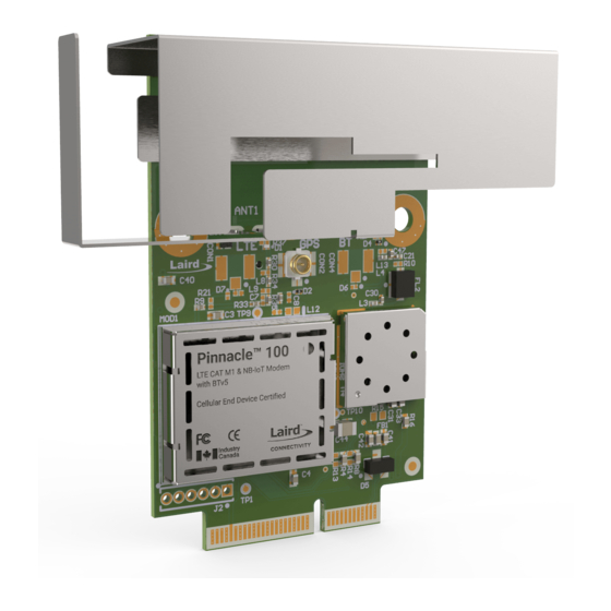
- Page 3 Overview ..................................... 4 Laird Connectivity Pinnacle™ 100 Development Kit Part Numbers ..................4 Package Contents ................................4 Pinnacle™ 100 Development Kit – Main Development Board ..................... 5 Key Features ................................5 Understanding the Development Board ..........................6 Pinnacle™ 100 Default Configuration and Jumper Settings ..................8 SIM Card Insertion ..............................
- Page 4 The Laird Connectivity Pinnacle™ 100 development kit provides a platform for rapid BLE and cellular connectivity prototyping, providing multiple options for the development of Cellular IoT, Bluetooth Low Energy (BLE) plus Near Field Communication (NFC) applications. This document describes the development board hardware, highlighting the setup and interfaces available to maximize user flexibility in developing these applications.
- Page 5 Debug and program NRF software using both an internal and an external serial wire debug (SWD)or trace interface ▪ GPS antenna ▪ Optional footprint for Microchip ATECC608A-SSHDA authentication IC (not populated) ▪ Optional Spare Level Shifter Americas: +1-800-492-2320 © Copyright 2020 Laird Connectivity. All Rights Reserved Europe: +44-1628-858-940 www..lairdconnect.com/wireless Hong Kong: +852 2923 0610...
- Page 6 Figure 1: Dev board contents and locations Americas: +1-800-492-2320 © Copyright 2020 Laird Connectivity. All Rights Reserved Europe: +44-1628-858-940 www..lairdconnect.com/wireless Hong Kong: +852 2923 0610...
- Page 7 Figure 2: Development board 453-00010-K1 (fitted with 453-00010 Pinnacle™ 100 modem with integrated antenna) Americas: +1-800-492-2320 © Copyright 2020 Laird Connectivity. All Rights Reserved Europe: +44-1628-858-940 www..lairdconnect.com/wireless Hong Kong: +852 2923 0610...
- Page 8 3. The default recommend power connection is USB with FTDI USB, J30 connected. Figure 3: Default Pinnacle™ 100 development board 453-00010-K1 jumper and switch settings (image for 453-00010) Americas: +1-800-492-2320 © Copyright 2020 Laird Connectivity. All Rights Reserved Europe: +44-1628-858-940 www..lairdconnect.com/wireless...
- Page 9 RF grounding for the modem. Loose screws can affect antenna performance. Figure 6 shows the process of attaching a 453-00011 modem to a DVK. Figure 6: Attaching a 453-00011 Pinnacle 100 modem to a DVK Americas: +1-800-492-2320 © Copyright 2020 Laird Connectivity. All Rights Reserved Europe: +44-1628-858-940 www..lairdconnect.com/wireless Hong Kong: +852 2923 0610...
- Page 10 Revie Flex and FlexPIFA antennas attached to a 453-00011 modem. Both antennas must be placed on plastic for proper operation Figure 8: External antenna attachment for 453-00011 Pinnacle 100 modem Americas: +1-800-492-2320 © Copyright 2020 Laird Connectivity. All Rights Reserved Europe: +44-1628-858-940 www..lairdconnect.com/wireless Hong Kong: +852 2923 0610...
- Page 11 The Power supply circuit uses load switches to isolate nets from each other, this allows the Buck-Boost Regulator to be bypassed when connecting 2AA batteries and to directly power the modem, the 1.8V regulator is enabled for IO support. Americas: +1-800-492-2320 © Copyright 2020 Laird Connectivity. All Rights Reserved Europe: +44-1628-858-940 www..lairdconnect.com/wireless...
- Page 12 Figure 13. JLINK USB, FTDI USB, and ATMEL SUPPLY switch Figure 12: SWD external header, debug select switch and analog switch U10 Americas: +1-800-492-2320 © Copyright 2020 Laird Connectivity. All Rights Reserved Europe: +44-1628-858-940 www..lairdconnect.com/wireless Hong Kong: +852 2923 0610...
- Page 13 Figure 14, shows both USB connectors and J10 must be connected when using J7, to provide 5V to the modem pin M2.9. Figure 14: NRF and HL7800 USB Americas: +1-800-492-2320 © Copyright 2020 Laird Connectivity. All Rights Reserved Europe: +44-1628-858-940 www..lairdconnect.com/wireless...
- Page 14 I/O and allows for IO re-assignment when the DIP switches are open. By Default, All DIP Switches are ON. The silkscreen next to the header indicates the M2.#. Figure 16: P1, P2, and P3 IO headers Americas: +1-800-492-2320 © Copyright 2020 Laird Connectivity. All Rights Reserved Europe: +44-1628-858-940 www..lairdconnect.com/wireless Hong Kong: +852 2923 0610...
- Page 15 Table 1: P1 and S1 signal mapping to M2 pins Header Position M2.# DVK Function Switch Position nBT_REST nLTE_RESET 1V8_SIM BAT_RTC CR2032 Battery P0.03_AIN1 P0.02_AIN0 P0.28_AIN4 VIN_ADC_EN P0.29_AIN5 VIN_ADC SIM_CLK SIM_IO Americas: +1-800-492-2320 © Copyright 2020 Laird Connectivity. All Rights Reserved Europe: +44-1628-858-940 www..lairdconnect.com/wireless Hong Kong: +852 2923 0610...
- Page 16 BME680 Sensor P0.27 BME680 Sensor HOST_UART_DTR 2, 4 J10 NRF USB NRF_USB_D+ NRF_USB_D- J10 NRF USB USB_5V J10 NRF USB SWDCLK SWDIO Americas: +1-800-492-2320 © Copyright 2020 Laird Connectivity. All Rights Reserved Europe: +44-1628-858-940 www..lairdconnect.com/wireless Hong Kong: +852 2923 0610...
- Page 17 USB_CTS M2.34, P0.08, (U5 pin 30) HOST_UART_TX (output) USB_TX M2.32, P0.06, (U5 pin 2) HOST_UART_RX (input) USB_RX Figure 18: UART connections schematic Americas: +1-800-492-2320 © Copyright 2020 Laird Connectivity. All Rights Reserved Europe: +44-1628-858-940 www..lairdconnect.com/wireless Hong Kong: +852 2923 0610...
- Page 18 LED5 (Red) ‘ON’ indicates the ATMEL SUPPLY switch is set to OFF. LED6 (Green) ‘ON’ indicates Internal SWD activity. Figure 20: LEDs schematic Americas: +1-800-492-2320 © Copyright 2020 Laird Connectivity. All Rights Reserved Europe: +44-1628-858-940 www..lairdconnect.com/wireless Hong Kong: +852 2923 0610...
- Page 19 C signal traces are pulled high on the development board. Figure 22 shows the schematic and DVK location. Figure 22: BEM680 sensor schematic Americas: +1-800-492-2320 © Copyright 2020 Laird Connectivity. All Rights Reserved Europe: +44-1628-858-940 www..lairdconnect.com/wireless Hong Kong: +852 2923 0610...
- Page 20 Pinnacle 100 current consumption. For normal operation, the jumper on J4 must be fitted (and is fitted by default). Americas: +1-800-492-2320 © Copyright 2020 Laird Connectivity. All Rights Reserved Europe: +44-1628-858-940 www..lairdconnect.com/wireless Hong Kong: +852 2923 0610...
- Page 21 Figure 25: J4 Current measurement header The NFC antenna input connector (J16) allows the Laird Connectivity supplied flex-PCB NFC antenna to be plugged in. The Pinnacle™ 100 modem NFC circuit uses two pins, M2.22 (NFC1) and M2.20 (NFC2) to connect the antenna. C37 (300pF) and C38 (300pF) are RF tuning elements for the flexi-PCB NFC antenna.
- Page 22 J11 Pin 5 to J12 Pin 5 J11 Pin 6 to J12 Pin 6 The USB-UART can be connected to the HL7800 Debug port instead. Americas: +1-800-492-2320 © Copyright 2020 Laird Connectivity. All Rights Reserved Europe: +44-1628-858-940 www..lairdconnect.com/wireless Hong Kong: +852 2923 0610...
- Page 23 All Laird Connectivity products are sold pursuant to the Laird Connectivity Terms and Conditions of Sale in effect from time to time, a copy of which will be furnished upon request. When used as a tradename herein, Laird means Laird PLC or one or more subsidiaries of Laird PLC.
Need help?
Do you have a question about the Pinnacle 100 and is the answer not in the manual?
Questions and answers