Table of Contents
Advertisement
Quick Links
Advertisement
Table of Contents

Subscribe to Our Youtube Channel
Related Manuals for Laird DVK-SU60-2230C


Summary of Contents for Laird DVK-SU60-2230C
- Page 1 User Guide M.2 Development Kit (DVK-SU60-2230C) Version 1.0...
- Page 2 DVK-SU60-2230C Development Kit User Guide EVISION ISTORY Version Date Notes Approver 29 July 2017 Initial Release Jay White Americas: +1-800-492-2320 Embedded Wireless Solutions Support Center: Europe: +44-1628-858-940 http://ews-support.lairdtech.com Hong Kong: +852 2923 0610 www.lairdtech.com/wireless © Copyright 2017 Laird. All Rights Reserved...
-
Page 3: Table Of Contents
1.11 LTE Coexistence ............................16 1.12 LED Indicator ............................17 Additional Documentation ..........................17 Appendix ................................17 Americas: +1-800-492-2320 Embedded Wireless Solutions Support Center: Europe: +44-1628-858-940 http://ews-support.lairdtech.com Hong Kong: +852 2923 0610 www.lairdtech.com/wireless © Copyright 2017 Laird. All Rights Reserved... -
Page 4: Overview
Wi-Fi applications. This manual is for Rev. 01 of the development PCB and relates to DVK-SU60-2230C-B0 on the PCB itself. The complete functionality of the development kit hardware requires the use of Laird 50- and 60-series firmware version v xx.xx.xx... -
Page 5: Key Features
▪ Three buttons and LEDs for user interaction. ▪ External 32 KHz oscillator for the sleep clock. Americas: +1-800-492-2320 Embedded Wireless Solutions Support Center: Europe: +44-1628-858-940 http://ews-support.lairdtech.com Hong Kong: +852 2923 0610 www.lairdtech.com/wireless © Copyright 2017 Laird. All Rights Reserved... -
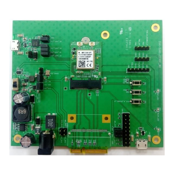
Page 6: Understanding The Development Board
Slide SW LED1 LED3 LED2 CON2 CON5 USB3 SDIO mPCIe DC Jack USB 2.0 Figure 1: Development board Americas: +1-800-492-2320 Embedded Wireless Solutions Support Center: Europe: +44-1628-858-940 http://ews-support.lairdtech.com Hong Kong: +852 2923 0610 www.lairdtech.com/wireless © Copyright 2017 Laird. All Rights Reserved... -
Page 7: Functional Blocks
PCIe Receive Data-Positive UART CTS I, PU 1.8V UART Clear-to-Send (Active low) PERn0 1.8V PCIe Receive Data-Negative VENDOR DEFINED38 Americas: +1-800-492-2320 Embedded Wireless Solutions Support Center: Europe: +44-1628-858-940 http://ews-support.lairdtech.com Hong Kong: +852 2923 0610 www.lairdtech.com/wireless © Copyright 2017 Laird. All Rights Reserved... - Page 8 RESERVED/PETp1 I2C CLK (O)(0/3.3V) RESERVED/PETn1 ALERT# (I)(0/3.3V) Ground RESERVED RESERVED/PERp1 UIM_SWP/PERST1# RESERVED/PERn1 UIM_POWER_SNK/CL KREQ1# Ground UIM_POWER_SRC/G PIO1/PEWAKE1# Americas: +1-800-492-2320 Embedded Wireless Solutions Support Center: Europe: +44-1628-858-940 http://ews-support.lairdtech.com Hong Kong: +852 2923 0610 www.lairdtech.com/wireless © Copyright 2017 Laird. All Rights Reserved...
-
Page 9: Sdio-Pin Header
Power 3.3V module power supply RESERVED/REFCLKn1 3.3V Power 3.3V module power supply Ground Ground Ground 3.1.2 SDIO-Pin Header Figure 2: DVK-SU60-2230C SDIO Pin Header Table 2: SDIO pin header Voltage If Not Name Type Description Used Ref. Ground SDIO DATA2 I/O, PU 1.8V... -
Page 10: Pcie Golden Finger
PCIe Transmit Data-Negative PCIE_3V3 Power 3.3V module power supply PETp0 1.8V PCIe Transmit Data-Positive Ground Ground Ground Americas: +1-800-492-2320 Embedded Wireless Solutions Support Center: Europe: +44-1628-858-940 http://ews-support.lairdtech.com Hong Kong: +852 2923 0610 www.lairdtech.com/wireless © Copyright 2017 Laird. All Rights Reserved... -
Page 11: Power Supply
Switch SW2 selects between the regulated 5 volt and USB. The voltage from host interface (PCIe or SDIO interface) is not regulated but is fed directly to M.2 module supply pin. Americas: +1-800-492-2320 Embedded Wireless Solutions Support Center: Europe: +44-1628-858-940 http://ews-support.lairdtech.com Hong Kong: +852 2923 0610 www.lairdtech.com/wireless © Copyright 2017 Laird. All Rights Reserved... -
Page 12: Tact Switch
Default position of SW2 is to select regulated 5 volts. The development board has a 1.8-volt regulator for the VCCIO of FTDI-Chip. Figure 4: DVK-SU60-2230C power supply for VCCIO of FTDI chip On the development board, the power domain: ▪... -
Page 13: Pcie_W_Disable_N (Sw5)
DVK-SU60-2230C Development Kit User Guide PCIE_W_DISABLE_N (SW5) PCIe host indication to disable the WLAN function of the device (Input) (Active Low) Figure 5: DVK-SU60-2230C 1.8V power supply 0 – Disable the WLAN 1 – Normal mode ▪ PCIE_W_DISABLE_N can accept an input of 3.3 volts. -
Page 14: Pmu_En (Sw7)
USB–UART – The development kit is fitted with a (U7) FTDI FT232R USB to UART converter which provides USB-to-Virtual COM port on any Windows PC (XP or later). Upon connection, Windows auto-installs the Americas: +1-800-492-2320 Embedded Wireless Solutions Support Center: Europe: +44-1628-858-940 http://ews-support.lairdtech.com Hong Kong: +852 2923 0610 www.lairdtech.com/wireless © Copyright 2017 Laird. All Rights Reserved... -
Page 15: Uart Interface Driven By External Source
Fit a jumper on J1 to disable the sleep clock, if needed. Figure 7: Pin header J1 Americas: +1-800-492-2320 Embedded Wireless Solutions Support Center: Europe: +44-1628-858-940 http://ews-support.lairdtech.com Hong Kong: +852 2923 0610 www.lairdtech.com/wireless © Copyright 2017 Laird. All Rights Reserved... -
Page 16: Pcm
Pin 3 COEX3 Pin 4 Note: is from 1.26V to 2.2V; V is from -0.4V to 0.54V. Americas: +1-800-492-2320 Embedded Wireless Solutions Support Center: Europe: +44-1628-858-940 http://ews-support.lairdtech.com Hong Kong: +852 2923 0610 www.lairdtech.com/wireless © Copyright 2017 Laird. All Rights Reserved... -
Page 17: Led Indicator
3.3V module power LED3 WLAN status (Active Low) DDITIONAL OCUMENTATION Laird offers a variety of documentation and ancillary information to support our customers through the initial evaluation process and ultimately into mass production. Additional documentation includes: ▪ DVK-SU60-2230C – User Manual ▪... - Page 18 Mouser Electronics Authorized Distributor Click to View Pricing, Inventory, Delivery & Lifecycle Information: Laird DVK-SU60-2230C DVK-ST60-2230C...
Need help?
Do you have a question about the DVK-SU60-2230C and is the answer not in the manual?
Questions and answers