Advertisement
Quick Links
Advertisement

Subscribe to Our Youtube Channel
Related Manuals for Laird BL654PA


Summary of Contents for Laird BL654PA
- Page 1 Version 1.0...
- Page 2 Version Date Notes Contributor(s) Approver 20 Aug 2019 Initial version Raj Khatri Jonathan Kaye https://www.lairdconnect.com/wireless- Americas: +1-800-492-2320 modules/bluetooth-modules © Copyright 2019 Laird. All Rights Reserved Europe: +44-1628-858-940 Hong Kong: +852 2923 0610...
- Page 3 Overview ..................................... 4 Laird BL654PA Development Kit Part Numbers ........................4 Package Contents ................................4 BL654PA Development Kit – Main Development Board ...................... 4 DVK-BL654 and DVK-BL654PA Differences ......................5 Key Features ................................5 Understanding the Development Board ..........................7 BL654PA Default Configuration and Jumper Settings ....................
- Page 4 Bluetooth Low Energy (BLE) plus Near Field Communication (NFC) applications. The Laird BLE development kit is designed to support the rapid development of applications and software for the BL654PA series of BLE modules featuring Laird’s innovative event driven programming language – smartBASIC. More information regarding this product series including a detailed module user’s guide and smartBASIC user guides are available on Laird’s...
- Page 5 The DVK-BL654PA development board is identical to the DVK-BL654 development board but with one modification – the PCB footprint added for the BL654PA module. Since the BL654PA module operating voltage range is 3.0V to 5.5V (whilst the BL654 is 1.8V to 5.5V), the following power selection switch positions cannot be used on the DVK-BL654PA.
- Page 6 – Atmel MCU by use of an analog switch to route the BL654PA UART (for those customers working with Nordic SDK). USB2 to Atmel to Atmel UART (via open solderbridges) to BL654PA UART. ▪ Current measuring options (BL654PA module only): –...
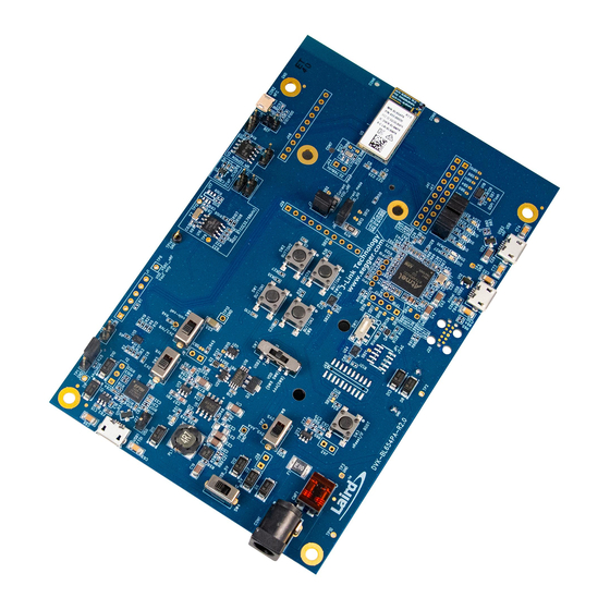
- Page 7 F USB I/F Figure 1: Dev board contents and locations Figure 2: Development board 455-00022 (fitted with 453-00020 BLE module with integrated antenna) https://www.lairdconnect.com/wireless- Americas: +1-800-492-2320 modules/bluetooth-modules © Copyright 2019 Laird. All Rights Reserved Europe: +44-1628-858-940 Hong Kong: +852 2923 0610...
- Page 8 (default) ONLY position Normal Voltage (VDD pin of (5V5_AAA) BL654PA) operation Figure 3: Correct BL654PA DVK board (455-00022 or 455-00023) jumper and switch settings - 455-00022 pictured https://www.lairdconnect.com/wireless- Americas: +1-800-492-2320 modules/bluetooth-modules © Copyright 2019 Laird. All Rights Reserved Europe: +44-1628-858-940...
- Page 9 USB2 USB type micro-B connector – If it requires the Atmel USB2-SWD (BL654PA) path ▪ USB3 USB type micro-B connector – If it requires the USB3 to USB (BL654PA) path ▪ External DC supply (2.5V-5.5V), into DC jack connector (CON1), ▪...
- Page 10 Option 3 – High voltage mode with voltage via USB3 For either high voltage option, if you use the BL654PA USB interface, the BL654PA VBUS pin must be connected to an external supply within the range of 4.35V to 5.5V.
- Page 11 No voltage is presented to VDD pin, as in High voltage mode, the VDD pin becomes an output voltage pin. It can be used to supply external circuitry from the VDD pin. Before any current can be taken from the BL654PA VDD pin, this feature must be enabled in the BL654PA.
- Page 12 VDD_nRFp (that is current going into header J7 pin 1). ▪ VDD_nRF – Supplies the BL654PA series module only and is to the current that has come out of the current measuring block on the development board on header connector J7 pin 2.
- Page 13 Dual OP,10uA/amp VSUPPLY VOUT R137 CONTROL VDD_nRF_SENSE Load-Switch-IC,1A VSUPPLY _EN VDD_nRF_SENSE SB24 NOPOP (Solderbridge_Open) DUAL-NCH,+20V,800mA Figure 5: Schematic and PCB location of SB24 https://www.lairdconnect.com/wireless- Americas: +1-800-492-2320 modules/bluetooth-modules © Copyright 2019 Laird. All Rights Reserved Europe: +44-1628-858-940 Hong Kong: +852 2923 0610...
- Page 14 The coin cell operation of BL654PA module on the DVK-BL654PA devboard is NOT possible. A J34 coin cell holder cannot be used on the DVK-BL654PA SW6 default and only valid position is 3V3/1V8. SW6 position coin cell is not valid for the BL654PA.
- Page 15 USB2 cable plugged in. The development board provides access to the BL654PA module two-wire SWD interface on JP1 via analog switch U24. This is required for customer use, since the BL654PA module supports smartBASIC runtime engine firmware over JTAG (as well as over UART).
- Page 16 Figure 10: USB2 to SWD onboard circuitry routing via analog switch (U24) Table 3 displays the four signals running from Atmel MCU U14 (SWD interface plus SIO_32 and nReset_BLE) to the BL654PA module (SWD interface plus SIO_32 and nReset_BLE). Table 3: USB U4 USB-SWD to BL654PA SWD signal routing connections...
- Page 17 UART Interface Driven by External UART Source: The BL654PA module UART interface (TX, RX, CTS, RTS) is presented at a 2.54 mm (0.1 in.) pitch header (J1). To allow the BL654PA UART interface to be driven from the breakout header connector (J1), the following must be configured: –...
- Page 18 UART TTL (3.3V) converter cable using J1. Fitting a jumper in J35 also allows the BL654PA UART to be routed to Atmel MCU UART (signal also on J19 and net names beginning with IMCU_) via open solder bridges SB16 to SB19 shown in Figure 13.
- Page 19 The J12 header connector allows the USB_DTR signal from the FTDI chip to be disconnected from the BL654PA. To connect the BL654PA nAutoRUN pin SIO_35 (pin 5) to PC FTDI USB_DTR line via the J12 header connector, do the following: ▪...
- Page 20 (SIO_35) must be configured to select between these two modes. ▪ VSP Bridge to UART mode takes data sent from phone or tablet (over BLE) and sends to BL654PA to be sent out of the BL654PA UART (therefore data not stored on BL654PA).
- Page 21 The development board connects the BL654PA module to a virtual COM port of a PC or other device. From a PC, you can Laird’s UwTerminalX communicate with the module using (cross platform software available for Windows, Mac, and Linux). This utility allows connections to serial devices using any combination of the communications parameters listed in...
- Page 22 Access to all 46 BL654PA series module signal pins (SIO’s = Signal Input /Output) is available on plated-through holes (for 2.54 mm pitch header connectors) on J44, J47, J48, J41, J29, J1, J12, J1, J5, J17, J21, J6, and J36.
- Page 23 J39 Connects SIO_16 to LED4 SIO_16 LED4 PIN HEADER,2.54mm 1X2P J39 jumper fitted (default). SIO_16 LED4 PIN HEADER,2.54mm 1X2P PIN HEADER,2.54mm 1X2P BL654PA pin plated holes for access: NOPOP (PIN HEADER,2.54mm 1X10P) ▪ SI0_ 28 SIO_28 ▪ SI0_ 29 SIO_29 ▪...
- Page 24 SWDIO_BLE SIO_41 on BL654PA is SPI_CLK (as an SWDCLK_BLE alternative function) is disconnected from J46 on SIO_32_SWO_BLE devboard by open solderbridge SB23. nRESET_BLE SIO_41 on BL654PA is directly connected to U2 SIO_07 TRACECLK SIO_32_SWO_BLE TRACEDATA0 (Eeprom) pin6 on devboard. SIO_12...
- Page 25 J21 pin 2-1 jumper NOT fitted (default). J6 routes SIO_03 to Temp Sensor Temp_Sens SIO_03 J6 pin 2-1 jumper NOT fitted (default) PIN HEADER,2.54mm 1X2P https://www.lairdconnect.com/wireless- Americas: +1-800-492-2320 modules/bluetooth-modules © Copyright 2019 Laird. All Rights Reserved Europe: +44-1628-858-940 Hong Kong: +852 2923 0610...
- Page 26 For more information on these sample applications, see GitHub smartBASIC sample applications repository on the BL654PA product page at https://github.com/LairdCP/BL654PA-Applications. The temperature sensor (U1) by default is connected to the BL654PA module as jumper on J6 pin bridges TEMP_SENS and SIO_03. Analog output temp sensor V+ 2.4V-3.6V...
- Page 27 +70ºC +1041.4mV +60ºC +1158.1mV +50ºC +1274.8mV +40ºC +1391.5mV +30ºC +1508.2mV +20ºC +1624.9mV +10ºC +1741.6mV +0ºC +1858.2mV -10ºC +1975.0mV -20ºC +2091.7mV -30ºC +2208.4mV https://www.lairdconnect.com/wireless- Americas: +1-800-492-2320 modules/bluetooth-modules © Copyright 2019 Laird. All Rights Reserved Europe: +44-1628-858-940 Hong Kong: +852 2923 0610...
- Page 28 The I2C RTC chip (U16) allows the BL654PA I2C interface to be tested. The output of the RTC chip (U16) is on the I2C bus and is by default connected to the BL654PA module via jumpers on J17 and J21.
- Page 29 Figure 17: SPI EEPROM schematic and PCB For a working example of the BL654PA SPI interface using the SPI EEPROM (U2), a smartBASIC application for this will be available in the future in the GitHub smartBASIC sample application repository on the BL654PA product page at https://github.com/LairdCP/BL654PA-Applications.
- Page 30 Refer to the smartBASIC application script example btn.button.led.test.sb in the GitHub smartBASIC sample application repository on the BL654PA product page at https://github.com/LairdCP/BL654PA-Applications The LEDs are active high, meaning that writing a logical one (“1”) to the output pin illuminates the LED.
- Page 31 The NFC antenna input connector (CON2) allows the Laird supplied flex-PCB NFC antenna to be plugged in. The BL654PA module NFC circuit uses two pins, pin 59 (NFC1/SIO_9) and pin 57 (NFC2/SIO_10) to connect the antenna. These pins are shared with GPIOs (SIO.09 and SIO.10). BL654PA NFC pins are enabled by default. NFC can be disabled via smartBASIC application.
- Page 32 Figure 20: Optional external serial SPI flash IC (U18) schematic and PCB Table 15 shows the U18 pin mapping to BL654PA SIO pin mapping (via open solder bridges). Table 15: U18 SPI or QSPI flashc IC pin mapping to BL654PA GPIO mappings...
- Page 33 (default) to stay within ±250 ppm. The BL654PA also allows, as an option, to connect an external higher accuracy (±20 ppm) 32.768 kHz crystal to the BL654PA-SX-xx pins SIO_01/XL2 (pin 41) and SIO_00/XL1 (pin 42). This provides improved protocol timing and helps with radio power consumption in the system standby doze/deep sleep modes by reducing the time that the Rx window must be open.
- Page 34 For normal operation, the jumper on J7 (and J9) must be fitted (and is fitted by default). IMPORTANT: To achieve the optimal power consumption of the BL654PA series module on the development board, see the “lp.low.power.deep.sleep.sb” file in the GitHub smartBASIC sample application repository on the BL654PA product page at https://github.com/LairdCP/BL654PA-Applications...
- Page 35 Additional documentation can be accessed from the Documentation tab of the Laird BL654PA Product Page. For any additional questions or queries, or to receive technical support for this Development Kit or for the BL654PA module series, please contact Embedded Wireless Solutions Support: https://www.lairdconnect.com/resources/support https://www.lairdconnect.com/wireless-...
- Page 36 All Laird products are sold pursuant to the Laird Terms and Conditions of Sale in effect from time to time, a copy of which will be furnished upon request. When used as a tradename herein, Laird means Laird PLC or one or more subsidiaries of Laird PLC.
Need help?
Do you have a question about the BL654PA and is the answer not in the manual?
Questions and answers