Table of Contents
Advertisement
Quick Links
Advertisement
Table of Contents

Subscribe to Our Youtube Channel
Related Manuals for Aaeon PICO-BT01


Summary of Contents for Aaeon PICO-BT01
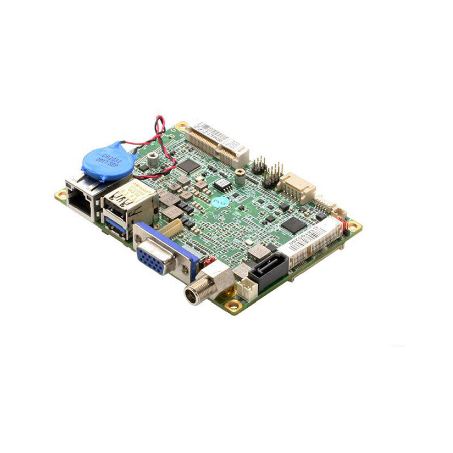
- Page 1 P I C O - B T 0 1 PICO-BT01 Intel® Atom Intel® I211 Ethernet 1 USB3.0, 2 USB2.0, 2 COM 4-bit Digital I/O 1 mSATA/ MiniCard (Full-size) 1 MiniCard (Half-size) BIO Connector for Daughterboard PICO-BT01 Rev. A Manual 1st Ed. January 23, 2015...
- Page 2 AAEON assumes no liabilities resulting from errors or omissions in this document, or from the use of the information contained herein. AAEON reserves the right to make changes in the product design without notice to its users.
- Page 3 P I C O - I T X B o a r d P I C O - B T 0 1 Acknowledgments All other products’ name or trademarks are properties of their respective owners. AMI is a trademark of American Megatrends Inc. ®...
- Page 4 Heat Spreader COMs + line-out cable DVD-ROM for Manual (in PDF Format) and Drivers PICO-BT01 If any of these items should be missing or damaged, please contact your distributor or sales representative immediately.
-
Page 5: Table Of Contents
P I C O - I T X B o a r d P I C O - B T 0 1 Contents Chapter 1 General Information 1.1 Introduction ..............1-2 1.2 Features ..............1-3 1.3 Specifications ............1-4 Chapter 2 Quick Installation Guide 2.1 Safety Precautions .......... - Page 6 P I C O - I T X B o a r d P I C O - B T 0 1 2.16 DP Port (CN4) ............2-21 2.17 LVDS Port Inverter / Backlight Connector (CN5) .. 2-22 2.18 LAN (RJ-45) Port (CN7) ........2-23 2.19 Digital IO Port (CN8) ..........
- Page 7 P I C O - I T X B o a r d P I C O - B T 0 1 Appendix A Programming The Watchdog Timer A.1 Watchdog Timer Registers ........A-2 A.2 Watchdog Sample Program ........A-3 Appendix B I/O Information B.1 I/O Address Map ............
-
Page 8: Chapter 1 General Information
P I C O - I T X B o a r d P I C O - B T 0 1 Chapter General Information 1- 1 Chapter 1 General Information... -
Page 9: Introduction
Display requirements are met with an abundance of interfaces such as VGA, DP and LVDS. The PICO-BT01 supports 18/24-bit LVDS with PWM function. With all of its integrated features, the PICO-BT01 strikes a balance of performance and price. This versatile product targets Industrial Automation, Entertainment, Networking, KIOSK/POS, Transportation, Banking, Healthcare and Digital Signage applications that require high performance and high reliability. -
Page 10: Features
P I C O - I T X B o a r d P I C O - B T 0 1 1.2 Features Intel® Atom™ E3845/E3825 SoC Up to 1.91 GHz 204-pin SODIMM DDR3L 1066/1333MHz up to 8GB ... -
Page 11: Specifications
P I C O - I T X B o a r d P I C O - B T 0 1 1.3 Specifications System From Factor PICO-ITX Processor Intel® Atom™ E3845/E3825 SoC Up to 1.91 GHz System Memory 204-pin SODIMM DDR3 1066/1333 MHz, up to 8 GB... - Page 12 P I C O - I T X B o a r d P I C O - B T 0 1 Operating Humidity 0% ~ 90% relative humidity, non-condensing Display: Supports CRT/TFT LCD/DP Chipset Intel Atom™ SoC ...
-
Page 13: Chapter 2 Quick Installation Guide
P I C O - I T X B o a r d P I C O - B T 0 1 Chapter Quick Installation Guide Chapter 2 Quick Installation Guide... -
Page 14: Safety Precautions
P I C O - I T X B o a r d P I C O - B T 0 1 2.1 Safety Precautions Always completely disconnect the power cord from your board whenever you are working on it. Do not make connections while the power is on, because a sudden rush of power can damage sensitive electronic components. -
Page 15: Location Of Connectors And Jumpers
P I C O - I T X B o a r d P I C O - B T 0 1 2.2 Location of Connectors and Jumpers Component Side Component Side Component Side Chapter 2 Quick Installation Guide... - Page 16 P I C O - I T X B o a r d P I C O - B T 0 1 Solder Side Solder Side Chapter 2 Quick Installation Guide...
-
Page 17: Mechanical Drawing
P I C O - I T X B o a r d P I C O - B T 0 1 2.3 Mechanical Drawing Component Side Component Side Component Side Chapter 2 Quick Installation Guide... - Page 18 P I C O - I T X B o a r d P I C O - B T 0 1 Solder Side Solder Side Chapter 2 Quick Installation Guide...
- Page 19 P I C O - I T X B o a r d P I C O - B T 0 1 Heat Spreader Chapter 2 Quick Installation Guide...
- Page 20 P I C O - I T X B o a r d P I C O - B T 0 1 Chapter 2 Quick Installation Guide...
- Page 21 P I C O - I T X B o a r d P I C O - B T 0 1 Chapter 2 Quick Installation Guide...
- Page 22 P I C O - I T X B o a r d P I C O - B T 0 1 2-10 Chapter 2 Quick Installation Guide...
- Page 23 P I C O - I T X B o a r d P I C O - B T 0 1 2-11 Chapter 2 Quick Installation Guide...
-
Page 24: Heat Spreader Installation
P I C O - I T X B o a r d P I C O - B T 0 1 2.4 Heat Spreader Installation Before Installation, please make sure to: Insert the RAM (DDR3L SODIMM RAM only) first as it will later be covered by the heat spreader ... - Page 25 P I C O - I T X B o a r d P I C O - B T 0 1 Turn the board over Place the heat spreader on the board and tighten the screws Place the heat sink (if any) on the heat spreader and tighten the screws 2-13 Chapter 2 Quick Installation Guide...
-
Page 26: List Of Jumpers
P I C O - I T X B o a r d P I C O - B T 0 1 2.5 List of Jumpers The board has a number of jumpers that allow you to configure your system to suit your application. The table below shows the function of each of the board's jumpers: Label Function... -
Page 27: List Of Connectors
P I C O - I T X B o a r d P I C O - B T 0 1 2.6 List of Connectors The board has a number of connectors that allow you to configure your system to suit your application. The table below shows the function of each board's connectors: Label F unction... - Page 28 P I C O - I T X B o a r d P I C O - B T 0 1 CN27 COM Port 1/2 & line out connector 2-16 Chapter 2 Quick Installation Guide...
-
Page 29: Setting Jumpers
P I C O - I T X B o a r d P I C O - B T 0 1 2.7 Setting Jumpers You configure your card to match the needs of your application by setting jumpers. A jumper is the simplest kind of electric switch. It consists of two metal pins and a small metal clip (often protected by a plastic cover) that slides over the pins to connect them. -
Page 30: Clear Cmos Jumper (Jp1 1,3,5)
P I C O - I T X B o a r d P I C O - B T 0 1 2.8 Clear CMOS Jumper (JP1 1,3,5) Normal (Default) Clear CMOS 2.9 Auto Power Button Enable/Disable Selection (JP1 2,4,6) Enable (Default) Disable 2.10 LVDS Port Operating Voltage Selection (JP3) -
Page 31: Lvds Backlight Lightness Control Mode Selection (Jp4 2,4,6)
P I C O - I T X B o a r d P I C O - B T 0 1 2.12 LVDS Backlight Lightness Control Mode Selection (JP4 2,4,6) PWM Mode VR Mode (Default) 2-19 Chapter 2 Quick Installation Guide... -
Page 32: Battery (Cn1)
P I C O - I T X B o a r d P I C O - B T 0 1 2.13 Battery (CN1) Pin Name Signal Type Signal Level +3.3V 3.3V 2.14 DDR3L SO-DIMM Slot (CN2) Standard specification 2.15 VGA Port (CN3) Pin Name Signal Type... -
Page 33: Dp Port (Cn4)
P I C O - I T X B o a r d P I C O - B T 0 1 Pin Name Signal Type Signal level DDC_DATA HSYNC VSYNC DDC_CLK 2.16 DP Port (CN4) Pin Name Signal Type Signal level DDI0_DP_D0_P DIFF... -
Page 34: Lvds Port Inverter / Backlight Connector (Cn5)
P I C O - I T X B o a r d P I C O - B T 0 1 DDI0_DP_D2_P DIFF DDI0_DP_D2_N DIFF DDI0_DP_D3_P DIFF DDI0_DP_D3_N DIFF DDI0_DP_AUX_P +3.3V DDI0_DP_AUX_N +3.3V HPLG_DETECT +1.8V RTN_PWR +3.3V 2.17 LVDS Port Inverter / Backlight Connector (CN5) BLK_PWR BKL_CONTROL BKL_ENABLE... -
Page 35: Lan (Rj-45) Port (Cn7)
P I C O - I T X B o a r d P I C O - B T 0 1 Pin Name Signal Type Signal Level BKL_PWR +5V / +12V BKL_CONTROL BKL_ENABLE +3.3V ※ LVDS2/BKL_PWR can be set to +5V or +12V by JP4. ※... -
Page 36: Digital Io Port (Cn8)
P I C O - I T X B o a r d P I C O - B T 0 1 DIFF MDI1- DIFF MDI3+ DIFF MDI3- 2.19 Digital IO Port (CN8) Pin Name Signal Type Signal Level DIO0 DIO1 DIO2 DIO3... - Page 37 P I C O - I T X B o a r d P I C O - B T 0 1 Pin Name Signal Type Signal level +1.5V +1.5V PCIE_CLK_REQ# UIM_PWR UIM_DATA PCIE_REF_CLK- DIFF UIM_CLK PCIE_REF_CLK+ DIFF UIM_RST UIM_VPP W_DISABLE# +3.3V PCIE_RST#...
- Page 38 P I C O - I T X B o a r d P I C O - B T 0 1 Pin Name Signal Type Signal level PCIE_RX-/mSATARX+ DIFF +3.3VSB/+3.3V +3.3V PCIE_RX+/mSATARX- DIFF +1.5V +1.5V SMB_CLK +3.3V PCIE_TX-/mSATATX- DIFF SMB_DATA +3.3V PCIE_TX+/mSATATX+...
-
Page 39: Usb Ports 0 And 1 (Cn10)
P I C O - I T X B o a r d P I C O - B T 0 1 Pin Name Signal Type Signal level +1.5V +1.5V +3.3VSB/+3.3V +3.3V 2.21 USB Ports 0 and 1 (CN10) Port 1 11 12 13 Port 0 2 3 4... - Page 40 P I C O - I T X B o a r d P I C O - B T 0 1 DIFF USB0_D+ USB0_SSRX− DIFF USB0_SSRX+ DIFF USB0_SSTX− DIFF USB0_SSTX+ DIFF +5VSB DIFF USB1_D- DIFF USB1_D+ ※ Only Port0 supports USB3.0. 2-28 Chapter 2 Quick Installation Guide...
-
Page 41: Usb 2.0 Port 3 (Cn11)
P I C O - I T X B o a r d P I C O - B T 0 1 2.22 USB 2.0 Port 3 (CN11) Pin Name Signal Type Signal Level +5VSB USB2_D- DIFF USB2_D+ DIFF 2.23 +5V Output for SATA HDD (CN14) Pin Name Signal Type Signal Level... -
Page 42: Sata Port (Cn15)
P I C O - I T X B o a r d P I C O - B T 0 1 2.24 SATA Port (CN15) Pin 1 Pin 7 Pin Name Signal Type Signal Level SATA_TX1+ DIFF SATA_TX1- DIFF SATA_RX1- DIFF SATA_RX1+... -
Page 43: Front Panel (Cn19)
P I C O - I T X B o a r d P I C O - B T 0 1 Pin Name Signal Type Signal Level +3.3V LAD0 +3.3V LAD1 +3.3V LAD2 +3.3V LAD3 +3.3V +3.3V LFRAME# +3.3V LRESET# LCLK LDRQ0... -
Page 44: External +12V Input (Cn20)
P I C O - I T X B o a r d P I C O - B T 0 1 SPEAKER- SPEAKER+ PWR_LED- PWR_LED+ H/W RESET- H/W RESET+ 2.27 External +12V Input (CN20) +12V GND Pin Name Signal Type Signal Level +12V +12V... - Page 45 P I C O - I T X B o a r d P I C O - B T 0 1 PS_ON# +5VSB +5VSB +5VSB +5VSB PCIE_REF_CLK0 RESET# PCIE_REF_CLK0# USBN0 USBP0 USBN1 USBP2 SMB_CLK SMB_DATA WAKE# 2-33 Chapter 2 Quick Installation Guide...
-
Page 46: Minicard Slot (Half-Mini Card) (Cn24)
P I C O - I T X B o a r d P I C O - B T 0 1 USB_OC0# USB_OC1# LPC_AD0 LPC_FRAME# LPC_AD1 SERIRQ LPC_AD2 LPC_DRQ LPC_AD3 GPIO0 AGND LPC_CLK AUD_LINEOUT_L PME# AUD_LINEOUT_R 2.30 MiniCard Slot (Half-Mini Card) (CN24) Pin Name Signal Type Signal Level... - Page 47 P I C O - I T X B o a r d P I C O - B T 0 1 PCIE_REF_CLK- DIFF PCIE_REF_CLK+ DIFF W_DISABLE# +3.3V PCIE_RST# +3.3V PCIE_RX- DIFF +3.3VSB +3.3V PCIE_RX+ DIFF +1.5V +1.5V 2-35 Chapter 2 Quick Installation Guide...
- Page 48 P I C O - I T X B o a r d P I C O - B T 0 1 SMB_CLK +3.3V PCIE_TX- DIFF SMB_DATA +3.3V PCIE_TX+ DIFF USB_D- DIFF USB_D+ DIFF +3.3VSB +3.3V +3.3VSB +3.3V +1.5V +1.5V 2-36 Chapter 2 Quick Installation Guide...
-
Page 49: Lvds Port (Cn25)
P I C O - I T X B o a r d P I C O - B T 0 1 +3.3VSB +3.3V 2.31 LVDS Port (CN25) Pin Name Signal Type Signal Level BKL_ENABLE BKL_CONTROL LCD_PWR +3.3V/+5V LVDS_A_CLK- DIFF LVDS_A_CLK+ DIFF LCD_PWR... -
Page 50: Com Port 1/2 & Line Out Connector (Cn27)
P I C O - I T X B o a r d P I C O - B T 0 1 LVDS_DA2+ DIFF LVDS_DA2- DIFF LVDS_DA3+ DIFF LVDS_DA3- DIFF DDC_CLK +3.3V DDC_DATA DDC_CLK 2.32 COM Port 1/2 & Line Out Connector (CN27) Pin Name Signal Type Signal Level... - Page 51 P I C O - I T X B o a r d P I C O - B T 0 1 RIB/+5V/+12V IN/ PWR +5V/+12V DCDA DSRA RTSA ±9V ±9V CTSA DTRA ±9V AGND LOUT_R LOUT_L COM port2 RS-485 Pin Name Signal Type Signal level...
- Page 52 P I C O - I T X B o a r d P I C O - B T 0 1 Pin Name Signal Type Signal level NC/+5V/+12V +5V/+12V GNDGND COM port2 RS-422 Pin Name Signal Type Signal level ±5V RS422_TX- ±5V...
-
Page 53: Electrical Specifications For I/O Port
P I C O - I T X B o a r d P I C O - B T 0 1 2.33 Electrical Specifications for I/O Port Signal Reference Rate Output Name VGA: +5V +5V/0.5A LVDS Port Inverter / +5V/2A or Backlight Connector +12V/2A... - Page 54 P I C O - I T X B o a r d P I C O - B T 0 1 China RoHS Requirements 产品中有毒有害物质或元素名称及含量 AAEON Main Board/ Daughter Board/ Backplane 有毒有害物质或元素 部件名称 铅 汞 镉 六价铬 多溴联苯 多溴二苯醚...
- Page 55 P I C O - I T X B o a r d P I C O - B T 0 1 Chapter BIOS Setup Chapter 3 AMI BIOS Setup 3-1...
-
Page 56: System Test And Initialization
4. The CMOS memory has lost power and the configuration information has been erased. The PICO-BT01 CMOS memory has an integral lithium battery backup for data retention. However, you will need to replace the complete unit when it finally runs down. -
Page 57: Ami Bios Setup
P I C O - I T X B o a r d P I C O - B T 0 1 3.2 AMI BIOS Setup AMI BIOS ROM has a built-in Setup program that allows users to modify the basic system configuration. This type of information is stored in battery-backed CMOS RAM and BIOS NVRAM so that it retains the Setup information when the power is turned off. - Page 58 P I C O - I T X B o a r d P I C O - B T 0 1 BIOS Setup Menu Main Press ‘Delete’ Key to enter Setup Chapter 3 AMI BIOS Setup 3-4...
- Page 59 P I C O - I T X B o a r d P I C O - B T 0 1 Advanced Chapter 3 AMI BIOS Setup 3-5...
- Page 60 P I C O - I T X B o a r d P I C O - B T 0 1 Advanced -> ACPI Settings Options summary: ACPI Sleep Suspend Disabled Optimal Default, Failsafe Default State S3 (Suspend to RAM) Select the highest ACPI sleep state the system will enter when the SUSPEND button is pressed.
- Page 61 P I C O - I T X B o a r d P I C O - B T 0 1 Power Mode ATX Type Optimal Default, Failsafe Default AT Type Select power supply mode Advanced -> F81801 Super IO Configuration Chapter 3 AMI BIOS Setup 3-7...
- Page 62 P I C O - I T X B o a r d P I C O - B T 0 1 Advanced -> Super IO Configuration Serial Port 1 Configuration Chapter 3 AMI BIOS Setup 3-8...
- Page 63 P I C O - I T X B o a r d P I C O - B T 0 1 Advanced -> Super IO Configuration Serial Port 2 Configuration Options summary: Serial Port Disabled Enabled Default Allows BIOS to En/Disable correspond serial port. Change Settings Auto Default...
- Page 64 P I C O - I T X B o a r d P I C O - B T 0 1 IO=2F8h; IRQ=3,4,5,6,7,9,10,11,12; IO=3E8h; IRQ=3,4,5,6,7,9,10,11,12; IO=2E8h; IRQ=3,4,5,6,7,9,10,11,12; Allows BIOS to Select Serial Port resource. Change Settings Auto Default (Serial Port 2) IO=2F8h;...
- Page 65 P I C O - I T X B o a r d P I C O - B T 0 1 Advanced -> H/W Monitor Chapter 3 AMI BIOS Setup 3-11...
- Page 66 P I C O - I T X B o a r d P I C O - B T 0 1 Advanced -> CPU Configuration Options summary: Intel Disabled Virtualization Enabled Optimal Default, Failsafe Default Technology When enabled, a VMM can utilize the additional hardware capabilities provided by Vander pool Technology Chapter 3 AMI BIOS Setup 3-12...
- Page 67 P I C O - I T X B o a r d P I C O - B T 0 1 Advanced -> CPU Configuration Socket 0 CPU Information Chapter 3 AMI BIOS Setup 3-13...
- Page 68 P I C O - I T X B o a r d P I C O - B T 0 1 Advanced -> SATA Configuration Options summary: Serial-ATA (SATA) Enabled Default Disabled En/Disable SATA SATA Speed Support Gen1 Default Gen2 SATA Speed Support Gen1 or Gen2 SATA Mode...
- Page 69 P I C O - I T X B o a r d P I C O - B T 0 1 IDE: Configure SATA controllers as legacy IDE AHCI: Configure SATA controllers to operate in AHCI mode Serial-ATA Port x Enabled Default Disabled...
- Page 70 P I C O - I T X B o a r d P I C O - B T 0 1 Advanced->Dynamic Digital IO Configuration Digital Port X Direction Input Output Set DIO as input or Output Digital Port X Level Default Set DIO Output port Hi or Low Chapter 3 AMI BIOS Setup 3-16...
- Page 71 P I C O - I T X B o a r d P I C O - B T 0 1 Advanced -> USB Configuration Options summary: Legacy USB Support Enabled Optimal Default, Failsafe Default Disabled Auto Enables BIOS Support for Legacy USB Support. When enabled, USB can be functional in legacy environment like DOS.
- Page 72 P I C O - I T X B o a r d P I C O - B T 0 1 Forced FDD Hard Disk CDROM If Auto. USB devices less than 530MB will be emulated as Floppy and remaining as Floppy and remaining as hard drive.
- Page 73 P I C O - I T X B o a r d P I C O - B T 0 1 Options summary: Wake system with Fixed Time Enable Disable Optimal Default, Failsafe Default Wake up hour Wake up minute 0 Wake up second 0 Wake system with Dynamic Enable...
- Page 74 P I C O - I T X B o a r d P I C O - B T 0 1 Chipset Chapter 3 AMI BIOS Setup 3-20...
- Page 75 P I C O - I T X B o a r d P I C O - B T 0 1 Chipset -> Host Bridge Options summary: Primary IGFX Boot VBIOS Default Optimal Default, Failsafe Default Display LVDS Select the Video device LVDS1 Disabled Enabled...
- Page 76 P I C O - I T X B o a r d P I C O - B T 0 1 800x480 800x600 1024x600 1024x768 Optimal Default, Failsafe Default 1280x768 1366x768 1440x900 Select panel type Color Depth 18Bit Optimal Default, Failsafe Default 24Bit Set color depth Backlight Type...
- Page 77 P I C O - I T X B o a r d P I C O - B T 0 1 Chipset -> South Bridge Options summary: PCIE/mSATA Select PCIE Optimal Default, Failsafe Default mSATA PCIE/mSATA Select Chapter 3 AMI BIOS Setup 3-23...
- Page 78 P I C O - I T X B o a r d P I C O - B T 0 1 Chipset -> South Bridge -> Azallia HD Audio Azalia HD Audio Disabled Enabled Optimal Default, Failsafe Default Enabling/Disabling HD Audio controller. Chapter 3 AMI BIOS Setup 3-24...
- Page 79 P I C O - I T X B o a r d P I C O - B T 0 1 Chipset -> South Bridge -> USB Configuration Chapter 3 AMI BIOS Setup 3-25...
- Page 80 P I C O - I T X B o a r d P I C O - B T 0 1 Chipset -> South Bridge -> PCI Express Configuration Options summary: PCI Express Root Port x Enabled Optimal Default, Failsafe Default Disabled Enabling/Disabling PCI Express root ports Chapter 3 AMI BIOS Setup 3-26...
- Page 81 P I C O - I T X B o a r d P I C O - B T 0 1 Security Setup submenu: Security Change User/Supervisor Password You can install a Supervisor password, and if you install a supervisor password, you can then install a user password.
- Page 82 P I C O - I T X B o a r d P I C O - B T 0 1 when the user enters the Setup utility. Removing the Password Highlight this item and type in the current password. At the next dialog box press Enter to disable password protection.
- Page 83 P I C O - I T X B o a r d P I C O - B T 0 1 Boot Options summary: Disabled Default Enabled En/Disable PXE boot for I211 LAN Quiet Boot Disabled Enabled Default En/Disable showing boot logo. Chapter 3 AMI BIOS Setup 3-29...
- Page 84 P I C O - I T X B o a r d P I C O - B T 0 1 Exit Chapter 3 AMI BIOS Setup 3-30...
-
Page 85: Chapter 4 Driver Installation
P I C O - I T X B o a r d P I C O - B T 0 1 Chapter D river Installation 4 -1 Chapter 4 Driver Installation... - Page 86 P I C O - I T X B o a r d P I C O - B T 0 1 The PICO-BT01 comes with an AutoRun DVD-ROM that contains all the drivers and utilities that needs to be installed.
- Page 87 P I C O - I T X B o a r d P I C O - B T 0 1 4.1 Installation Insert the PICO-BT01 DVD-ROM into the disk drive. And install the drivers from Step 1 to Step 7 in order. Step 1 – Install Chipset Driver 1.
- Page 88 P I C O - I T X B o a r d P I C O - B T 0 1 Win7_8-32_64_R273.exe file 2. Follow the instructions 3. Driver will be installed automatically Step 5 – Install TXE Driver 1.
-
Page 89: Appendix A Programming The Watchdog Timer
P I C O - I T X B o a r d P I C O - B T 0 1 Appendix Programming the Watchdog Timer Appendix A Programming the Watchdog Timer... -
Page 90: Watchdog Timer Registers
P I C O - I T X B o a r d P I C O - B T 0 1 A.1 Watchdog Timer Registers Table 1 : Watch dog relative IO address Default Value Note I/O Base I/O Base address for Watchdog operation. 0xA00 Address This address is assigned by SIO LDN7, register 0x60-0x61. -
Page 91: Watchdog Sample Program
P I C O - I T X B o a r d P I C O - B T 0 1 A.2 WatchDog Sample Program ****************************************************************************** // WDT I/O operation relative definition (Please reference to Table 1) #define WDTAddr 0xA00 // WDT I/O base address Void WDTWriteByte(byte Register, byte Value);... - Page 92 P I C O - I T X B o a r d P I C O - B T 0 1 ******************************************************************************* ******************************************************************************* // Procedure : AaeonWDTEnable VOID AaeonWDTEnable (){ WDTEnableDisable(1); // Procedure : AaeonWDTConfig VOID AaeonWDTConfig (byte Counter, BOOLEAN Unit){ // Disable WDT counting WDTEnableDisable(0);...
- Page 93 P I C O - I T X B o a r d P I C O - B T 0 1 // Watchdog WDTRST# Enable WDTSetBit(DevReg, WDTRstBit, WDTRstVal); VOID WDTClearTimeoutStatus(){ WDTSetBit(TimerReg, StatusBit, 1); ******************************************************************************* ******************************************************************************* VOID WDTWriteByte(byte Register, byte Value){ IOWriteByte(WDTAddr+Register, Value);...
-
Page 94: Appendix B I/O Information
P I C O - I T X B o a r d P I C O - B T 0 1 Appendix I/O Information Appendix B I/O Information... -
Page 95: I/O Address Map
P I C O - I T X B o a r d P I C O - B T 0 1 B.1 I/O Address Map Appendix B I/O Information... -
Page 96: Memory Address Map
P I C O - I T X B o a r d P I C O - B T 0 1 B.2 Memory Address Map Appendix B I/O Information... -
Page 97: Irq Mapping Chart
P I C O - I T X B o a r d P I C O - B T 0 1 B.3 IRQ Mapping Chart Appendix B I/O Information... - Page 98 P I C O - I T X B o a r d P I C O - B T 0 1 Appendix B I/O Information...
- Page 99 P I C O - I T X B o a r d P I C O - B T 0 1 Appendix B I/O Information...
- Page 100 P I C O - I T X B o a r d P I C O - B T 0 1 Appendix B I/O Information...
- Page 101 P I C O - I T X B o a r d P I C O - B T 0 1 Appendix B I/O Information...
- Page 102 P I C O - I T X B o a r d P I C O - B T 0 1 Appendix B I/O Information...
- Page 103 P I C O - I T X B o a r d P I C O - B T 0 1 B-10 Appendix B I/O Information...
- Page 104 P I C O - I T X B o a r d P I C O - B T 0 1 B-11 Appendix B I/O Information...
- Page 105 P I C O - I T X B o a r d P I C O - B T 0 1 B-12 Appendix B I/O Information...
- Page 106 P I C O - I T X B o a r d P I C O - B T 0 1 B-13 Appendix B I/O Information...
- Page 107 P I C O - I T X B o a r d P I C O - B T 0 1 B-14 Appendix B I/O Information...
- Page 108 P I C O - I T X B o a r d P I C O - B T 0 1 B-15 Appendix B I/O Information...
-
Page 109: Appendix C Mating Connector
P i c o - s i z e S B C P I C O - B T 0 1 Appendix Mating Connector C - 1 Appendix C Mating Connector... -
Page 110: List Of Mating Connectors And Cables
F u l l - s i z e S B C F S B - B 7 5 G C.1 List of Mating Connectors and Cables The table notes mating connectors and available cables. Connector Function Mating Connector Available Cable P/N Label Cable... - Page 111 P i c o - s i z e S B C P I C O - B T 0 1 CN18 LPC Port PINREX 710-73-12TW01 AAEON 1703120130 Cable CN19 Front PINREX 222-97-05GBE1 Front 1701100156 Panel Panel Connector Cable CN20...
Need help?
Do you have a question about the PICO-BT01 and is the answer not in the manual?
Questions and answers