
Related Manuals for Aaeon PICO-KBU4


Summary of Contents for Aaeon PICO-KBU4
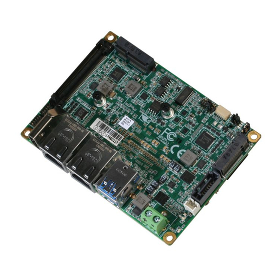
- Page 1 PICO-KBU4 PICO-KBU4 Single-Board Computer User’s Manual 1 Last Updated: April 10, 2018...
- Page 2 AAEON assumes no liabilities resulting from errors or omissions in this document, or from the use of the information contained herein. AAEON reserves the right to make changes in the product design without notice to its users.
- Page 3 Acknowledgement All other products’ name or trademarks are properties of their respective owners. Microsoft Windows is a registered trademark of Microsoft Corp. ® ITE is a trademark of Integrated Technology Express, Inc. IBM, PC/AT, PS/2, and VGA are trademarks of International Business Machines ...
- Page 4 Packing List Before setting up your product, please make sure the following items have been shipped: Item Quantity PICO-KBU4 Product DVD with drivers If any of these items are missing or damaged, please contact your distributor or sales representative immediately.
- Page 5 (if any), its specifications, dimensions, jumper/connector settings/definitions, and driver installation instructions (if any), to facilitate users in setting up their product. Users may refer to the AAEON.com for the latest version of this document. Preface...
- Page 6 Safety Precautions Please read the following safety instructions carefully. It is advised that you keep this manual for future references All cautions and warnings on the device should be noted. Make sure the power source matches the power rating of the device. Position the power cord so that people cannot step on it.
- Page 7 If any of the following situations arises, please the contact our service personnel: Damaged power cord or plug Liquid intrusion to the device iii. Exposure to moisture Device is not working as expected or in a manner as described in this manual The device is dropped or damaged Any obvious signs of damage displayed on the device...
- Page 8 FCC Statement This device complies with Part 15 FCC Rules. Operation is subject to the following two conditions: (1) this device may not cause harmful interference, and (2) this device must accept any interference received including interference that may cause undesired operation.
- Page 9 China RoHS Requirements (CN) 产品中有毒有害物质或元素名称及含量 AAEON Main Board/ Daughter Board/ Backplane 有毒有害物质或元素 部件名称 铅 汞 镉 六价铬 多溴联苯 多溴二苯醚 (Pb) (Hg) (Cd) (Cr(VI)) (PBB) (PBDE) 印刷电路板 ○ ○ ○ ○ ○ ○ 及其电子组件 外部信号 ○ ○ ○ ○ ○ ○...
- Page 10 China RoHS Requirement (EN) Poisonous or Hazardous Substances or Elements in Products AAEON Main Board/ Daughter Board/ Backplane Poisonous or Hazardous Substances or Elements Hexavalent Polybrominated Polybrominated Component Lead Mercury Cadmium Chromium Biphenyls Diphenyl Ethers (Pb) (Hg) (Cd) (Cr(VI)) (PBB) (PBDE) PCB &...
-
Page 11: Table Of Contents
Table of Contents Chapter 1 - Product Specifications..................1 Specifications ......................2 Chapter 2 – Hardware Information ..................4 Dimensions ....................... 5 Jumpers and Connectors ..................7 List of Jumpers ......................9 2.3.1 LVDS Backlight Lightness Control Mode Selection (JP3) ....10 2.3.2 LVDS Operating Voltage Selection (JP4) .......... - Page 12 2.4.15 SATA Port (CN20) ..................33 2.4.16 +5V Output for SATA HDD (CN21) ............34 2.4.17 M.2 (Key B) Connector (CN26) ............. 34 2.4.18 Smart FAN Connector (CN27) .............. 38 2.4.19 M.2 (Key E) Connector (CN30) ............. 38 2.4.20 DDR4 SO-DIMM Slot (DIMM1) ............41 2.5 Function Block ......................
- Page 13 Setup submenu: Security ..................67 Setup submenu: Boot ................... 68 3.7.1 BBS Priorities ....................69 Setup submenu: Exit ..................... 70 Chapter 4 – Drivers Installation ..................... 71 Product CD/DVD ....................72 Appendix A - Watchdog Timer Programming ..............74 Watchdog Timer Registers .................. 75 Watchdog Sample Program ................
-
Page 14: Chapter 1 - Product Specifications
Chapter 1 Chapter 1 - Product Specifications... -
Page 15: Specifications
Specifications System PICO-ITX Form Factor 7th Generation Intel® Core™ i processor U Processor series, Intel® i7-7600U, i5-7300U, i3-7100U series & Celeron® 3965U DDR4 1866/2133MHz SODIMM x 1, Max. 16 GB System Memory 7th Generation Intel® Core™ i processor U Chipset ... - Page 16 Operation Humidity 0 ~ 90% relative humidity, non-condensing Display 7th Generation Intel® Core™ i processor U Chipset series, Intel® i7-7600U, i5-7300U, i3-7100U series & Celeron® 3965U LVDS (18/24-bit 2CH) 1920 x 1200 HDMI 1.4b up Resolution to 4096 x 2304 (4K) DDI (BIO) LCD Interface 18/24-bit 2CH LVDS ...
-
Page 17: Chapter 2 - Hardware Information
Chapter 2 Chapter 2 – Hardware Information... -
Page 18: Dimensions
Dimensions Component Side Component Side Chapter 2 – Hardware Information... - Page 19 Solder Side Solder Side Chapter 2 – Hardware Information...
-
Page 20: Jumpers And Connectors
Jumpers and Connectors Component Side Component Side Chapter 2 – Hardware Information... - Page 21 Solder Side Solder Side Chapter 2 – Hardware Information...
-
Page 22: List Of Jumpers
List of Jumpers Please refer to the table below for all of the board’s jumpers that you can configure for your application Label Function LVDS Backlight Lightness Control Mode Selection LVDS Operating Voltage Selection LVDS Backlight Inverter Voltage Selection Clear CMOS Jumper Auto Power Button Enable/Disable Selection Chapter 2 –... -
Page 23: Lvds Backlight Lightness Control Mode Selection (Jp3)
2.3.1 LVDS Backlight Lightness Control Mode Selection (JP3) PWM Mode VR Mode(Default) 2.3.2 LVDS Operating Voltage Selection (JP4) +3.3V (Default) 2.3.3 LVDS Backlight Inverter Voltage Selection (JP4) +12V (Default) 2.3.4 Clear CMOS Jumper (JP5) Clear CMOS Normal (Default) Chapter 2 – Hardware Information... -
Page 24: Auto Power Button Enable/Disable Selection (Jp5)
2.3.5 Auto Power Button Enable/Disable Selection (JP5) Enable Auto Power Button Disable Auto Power Button (Default) Chapter 2 – Hardware Information... -
Page 25: List Of Connectors
List of Connectors Please refer to the table below for all of the board’s connectors that you can configure for your application Label Function RTC Battery Connector HDMI LVDS Inverter / Backlight Connector LVDS Port LAN (RJ-45) Port1 LAN (RJ-45) Port2 Digital IO Port CN10 USB 2.0 Port 1/2... -
Page 26: Rtc Battery Connector (Cn1)
2.4.1 RTC Battery Connector (CN1) Pin Name Signal Type Pin Name +3.3V +3.3V 2.4.2 HDMI (CN2) Pin Name Signal Type Signal level HDMI_TX2+ DIFF HDMI_TX2- DIFF Chapter 2 – Hardware Information... - Page 27 Pin Name Signal Type Signal level HDMI_TX1+ DIFF HDMI_TX1- DIFF HDMI_TX0+ DIFF HDMI_TX0- DIFF HDMI_CLK+ DIFF HDMI_CLK- DIFF DDC_CLK DDC_DATA HDMI_HPD Chapter 2 – Hardware Information...
-
Page 28: Lvds Inverter / Backlight Connector (Cn4)
2.4.3 LVDS Inverter / Backlight Connector (CN4) Pin Name Signal Type Signal Level BKL_PWR +5V / +12V BKL_CONTROL BKL_ENABLE +3.3V ※ LVDS/BKL_PWR can be set to +5V or +12V by JP4. ※ LVDS/BKL_CONTROL can be set by JP3. ※ The driving current supports up to 1A. Chapter 2 –... -
Page 29: Lvds Port (Cn5)
2.4.4 LVDS Port (CN5) ※ LVDS LCD_PWR can be set to +3.3V or +5V by JP4. ※ The max. driving current is 1A. Pin Name Signal Type Signal Level BKL_ENABLE BKL_CONTROL LCD_PWR +3.3V/+5V LVDS_A_CLK- DIFF LVDS_A_CLK+ DIFF LCD_PWR +3.3V/+5V LVDS_DA0- DIFF LVDS_DA0+ DIFF... - Page 30 DDC_CLK +3.3V LVDS_DB0- DIFF LVDS_DB0+ DIFF LVDS_DB1- DIFF LVDS_DB1+ DIFF LVDS_DB2- DIFF LVDS_DB2+ DIFF LVDS_DB3- DIFF LVDS_DB3+ DIFF LCD_PWR +3.3V/+5V LVDS_B_CLK- DIFF LVDS_B_CLK+ DIFF Chapter 2 – Hardware Information...
-
Page 31: Lan (Rj-45) Port1 (Cn6)
2.4.5 LAN (RJ-45) Port1 (CN6) Pin Name Signal Type Signal Level DIFF MDI0+ DIFF MDI0- DIFF MDI1+ DIFF MDI2+ DIFF MDI2- DIFF MDI1- DIFF MDI3+ DIFF MDI3- Chapter 2 – Hardware Information... -
Page 32: Lan (Rj-45) Port2 (Cn7)
2.4.6 LAN (RJ-45) Port2 (CN7) Pin Name Signal Type Signal Level MDI0+ DIFF MDI0- DIFF MDI1+ DIFF MDI2+ DIFF MDI2- DIFF MDI1- DIFF MDI3+ DIFF MDI3- DIFF Chapter 2 – Hardware Information... -
Page 33: Digital Io Port (Cn9)
2.4.7 Digital IO Port (CN9) Pin Name Signal Type Signal Level DIO_0 IN/OUT DIO_1 IN/OUT DIO_2 IN/OUT DIO_3 IN/OUT Chapter 2 – Hardware Information... -
Page 34: Usb 2.0 Port 1/2 (Cn10)
2.4.8 USB 2.0 Port 1/2 (CN10) Pin Name Signal Type Signal Level +V5SB +V5SB USB1_D- DIFF USB2_D- DIFF USB1_D+ DIFF USB2_D+ DIFF Chapter 2 – Hardware Information... -
Page 35: Usb 2.0/3.0 Port 3 Port 3/4 (Cn11)
2.4.9 USB 2.0/3.0 Port 3 Port 3/4 (CN11) Port 1 11 12 13 Port 0 2 3 4 Pin Name Signal Type Signal Level +V5SB USB3_D- DIFF USB3_D+ DIFF USB3_SSRX− DIFF USB3_SSRX+ DIFF USB3_SSTX− DIFF USB3_SSTX+ DIFF +V5SB USB4_D- DIFF USB4_D+ DIFF USB4_SSRX−... -
Page 36: External +12V Input (Cn14)
USB4_SSTX+ DIFF 2.4.10 External +12V Input (CN14) +12V GND Pin Name Signal Type Signal Level +12V +12V Chapter 2 – Hardware Information... -
Page 37: Front Panel Port (Cn15)
2.4.11 Front Panel Port (CN15) Pin Name Signal Type Signal level EXT_PWRBTN# SATA_LED- SATA_LED+ BUZZER- BUZZER+ PWR_LED+ HWRST# Chapter 2 – Hardware Information... -
Page 38: Com Port1/ Com Port2 (Cn16)
2.4.12 COM Port1/ COM Port2 (CN16) Pin Name Signal Type Signal Level LOUT_L LOUT_R AGND DCDA DCDB ±9V ±9V DTRA ±9V DTRB ±9V DSRA DSRB RTSA ±9V RTSB ±9V Chapter 2 – Hardware Information... - Page 39 CTSA CTSB RIA/+5V/+12V IN/ PWR +5V/+12V RIB/+5V/+12V IN/ PWR +5V/+12V COM Port 2 RS-422 Pin Name Signal Type Signal Level ±5V RS422_TX- ±5V RS422_TX+ RS422_RX+ RS422_RX- COM Port 2 RS-485 Pin Name Signal Type Signal Level RS485_D- ±5V RS485_D+ ±5V ※...
-
Page 40: Bio Bank1 Connector (Cn17)
2.4.13 BIO Bank1 Connector (CN17) Pin Name Signal Type Signal Level +12V +12V PCIE9_TXN DIFF PCIE9_RXN DIFF PCIE9_TXP DIFF PCIE9_RXP DIFF Chapter 2 – Hardware Information... - Page 41 Pin Name Signal Type Signal Level PCIE10_TXN DIFF PCIE10_RXN DIFF PCIE10_TXP DIFF PCIE10_RXP DIFF PS_ON# DDI1_CTRL_CLK DDI1_CTRL_DATA IN/OUT +V5A +V5A +V5A +V5A CLK_PCIE_P4 DIFF BUF_PLT_RST# CLK_PCIE_N4 DIFF DDI1_LANE1_DN Chapter 2 – Hardware Information...
- Page 42 Pin Name Signal Type Signal Level DDI1_LANE0_DN DDI1_LANE1_DP DDI1_LANE0_DP DDI1_LANE3_DN DDI1_LANE2_DN DDI1_LANE3_DP DDI1_LANE2_DP DDI1_HPD DDI1_AUX_DN DDI1_AUX_DP USB3_4_TXN IN/OUT USB3_4_TXP IN/OUT USB2N_4 IN/OUT Chapter 2 – Hardware Information...
- Page 43 Pin Name Signal Type Signal Level USB2P_4 IN/OUT USB3_4_RXN IN/OUT USB3_4_RXP IN/OUT SMB_CLK +3.3V SMB_DATA IN/OUT +3.3V PCIE_WAKE# USB2_OC3# +V5S USB2_OC3# +V5S +V5S +V5S +V5S LPC_AD0 IN/OUT LPC_FRAME# LPC_AD1 IN/OUT INT_SERIRQ IN/OUT Chapter 2 – Hardware Information...
- Page 44 Pin Name Signal Type Signal Level LPC_AD2 IN/OUT LPC_AD3 IN/OUT BIO_PWR_OK AUD_GND LPC_CLK_BIO LOUT_L PME# LOUT_R Chapter 2 – Hardware Information...
-
Page 45: Lpc Port (Cn19)
2.4.14 LPC Port (CN19) Pin Name Signal Type Signal Level IN/OUT +3.3V LAD0 IN/OUT +3.3V LAD1 IN/OUT +3.3V LAD2 IN/OUT +3.3V LAD3 +3.3V +V3.3S LFRAME# +3.3V LRESET# LCLK IN/OUT SMB_DATA/ I2C_SDA Chapter 2 – Hardware Information... -
Page 46: Sata Port (Cn20)
SMB_CLK/ I2C_CLK +3.3V SMB_ALERT/ INT_SERIRQ 2.4.15 SATA Port (CN20) Pin Name Signal Type Signal Level SATA_TX+ DIFF SATA_TX- DIFF SATA_RX- DIFF SATA_RX+ DIFF Chapter 2 – Hardware Information... -
Page 47: Output For Sata Hdd (Cn21)
2.4.16 +5V Output for SATA HDD (CN21) Pin Name Signal Type Signal Level +V5S 2.4.17 M.2 (Key B) Connector (CN26) Pin Name Signal Type Signal Level +V3.3S +3.3V +V3.3S +3.3V USB2P_10 IN/OUT W_DISABLE0# USB2N_10 IN/OUT SSD_LED# Chapter 2 – Hardware Information... - Page 48 PCIE11_RXN DIFF PCIE11_RXP DIFF PCIE11_TXN DIFF PCIE11_TXP DIFF SATA2_RXP DIFF Chapter 2 – Hardware Information...
- Page 49 SATA2_RXN DIFF SATA2_TXN DIFF SATA2_TXP DIFF BUF_PLT_RST# PCIE_CLK_REQ3# PCIE3_CLKN DIFF PCIE_WAKE# PCIE3_CLKP DIFF Chapter 2 – Hardware Information...
- Page 50 +V3.3S +3.3V +V3.3S +3.3V +V3.3S +3.3V Chapter 2 – Hardware Information...
-
Page 51: Smart Fan Connector (Cn27)
2.4.18 Smart FAN Connector (CN27) Pin Name Signal Type Signal Level +V3.3S +12V TACH 2.4.19 M.2 (Key E) Connector (CN30) Pin Name Signal Type Signal Level +V3.3A +3.3V USB2P_5 IN/OUT +V3.3A +3.3V USB2N_5 IN/OUT Chapter 2 – Hardware Information... - Page 52 PCIE1_TXP DIFF PCIE1_TXN DIFF Chapter 2 – Hardware Information...
- Page 53 PCIE1_RXP DIFF PCIE1_RXN DIFF PCIE1_CLKP DIFF PCIE1_CLKN DIFF BUF_PLT_RST# PCIE_CLK_REQ1# W_DISABLE1# PCIE_WAKE# W_DISABLE2# Chapter 2 – Hardware Information...
-
Page 54: Ddr4 So-Dimm Slot (Dimm1)
+V3.3S +3.3V +V3.3S +3.3V 2.4.20 DDR4 SO-DIMM Slot (DIMM1) Standard specification Chapter 2 – Hardware Information... -
Page 55: Function Block
2.5 Function Block Chapter 2 – Hardware Information... -
Page 56: Assembly Options
2.6 Assembly Options Option1 (Part Number:PICO-KBU4-FAN01) Chapter 2 – Hardware Information... - Page 57 Option2(Part Number:PICO-KBU4-HSK01) Chapter 2 – Hardware Information...
-
Page 58: Chapter 3 - Ami Bios Setup
Chapter 3 Chapter 3 - AMI BIOS Setup... -
Page 59: System Test And Initialization
System Test and Initialization These routines test and initialize board hardware. If the routines encounter an error during the tests, you will either hear a few short beeps or see an error message on the screen. There are two kinds of errors: fatal and non-fatal. The system can usually continue the boot up sequence with non-fatal errors. -
Page 60: Ami Bios Setup
AMI BIOS Setup AMI BIOS ROM has a built-in Setup program that allows users to modify the basic system configuration. This type of information is stored in battery-backed CMOS RAM and BIOS NVRAM so that it retains the Setup information when the power is turned off. Entering Setup Power on the computer and press <Del>or <ESC>... -
Page 61: Setup Submenu: Main
Setup Submenu: Main Chapter 3 – AMI BIOS Setup... -
Page 62: Setup Submenu: Advanced
Setup Submenu: Advanced Chapter 3 – AMI BIOS Setup... -
Page 63: Cpu Configuration
3.4.1 CPU configuration Options summary: Hyper-Threading Disabled Enabled Optimal Default, Failsafe Default Enable for Linux and Disabled for other OS. Active Processor Optimal Default, Failsafe Default Cores Number of cores to enable in each processor package. Intel (VMX) Disabled Virtualization Enabled Optimal Default, Failsafe Default Technology... - Page 64 Enabled Optimal Default, Failsafe Default Allows more then two frequency ranges to be supported. Turbo Mode Disabled Enabled Optimal Default, Failsafe Default Enable/Disable processor turbo mode. AUTO means enabled, unless max turbo ratio is bigger than 16 – SKL A0 W/A Chapter 3 –...
-
Page 65: Sata Configuration
3.4.2 SATA Configuration Options summary: SATA Controller(s) Enabled Optimal Default, Failsafe Default Disabled Enable or disable SATA Device. Port X Disabled Enabled Optimal Default, Failsafe Default Enable or Disable SATA Port. Hot Plug Disabled Optimal Default, Failsafe Default Enabled Designates this port as Hot Pluggable. Chapter 3 –... -
Page 66: Hardware Monitor
3.4.3 Hardware Monitor Chapter 3 – AMI BIOS Setup... -
Page 67: Cpu Smart Fan Mode Configuration
3.4.3.1 CPU Smart Fan Mode Configuration Options summary: Smart Fan1 Type Use linear fan application circuit. Output PWM mode (open Optimal Default, Failsafe Default drain) to control 4-wire fans. Smart fan type Fan Mode Manual Duty Auto Duty Optimal Default, Failsafe Default Smart fan mode Temperature Optimal Default, Failsafe Default... -
Page 68: Sio Configuration
3.4.4 SIO Configuration Chapter 3 – AMI BIOS Setup... -
Page 69: Serial Port Configuration
3.4.4.1 Serial Port Configuration Options summary: Use This Device Disabled Enabled Optimal Default, Failsafe Default En/Disable Serial Port (COM) Possible: Use Automatic Settings Optimal Default, Failsafe Default IO=2F8; IRQ=3; IO=3F8; IRQ=4; Select an optimal setting for IO device Mode: RS232 Optimal Default, Failsafe Default RS422;... -
Page 70: Usb Configuration
3.4.5 USB Configuration Options summary: Legacy USB Support Enabled Optimal Default, Failsafe Default Disabled Auto Enables BIOS Support for Legacy USB Support. When enabled, USB can be functional in legacy environment like DOS. AUTO option disables legacy support if no USB devices are connected Device Name (Emulation Auto Optimal Default, Failsafe Default... -
Page 71: Digital Io Port Configuration
3.4.6 Digital IO Port Configuration Options summary: DIO Port* Output Input Set DIO as Input or Output Output Level High Optimal Default, Failsafe Default Set output level when DIO pin is output Chapter 3 – AMI BIOS Setup... -
Page 72: Power Management
3.4.7 Power management Options summary: Power Mode ATX Type Optimal Default, Failsafe Default AT Type Select power supply mode. Restore on Power Last State Loss Always On Always Off Optimal Default, Failsafe Default Select power state when power is re-applied after a power failure. RTC wake system Disabled Optimal Default, Failsafe Default... -
Page 73: Firmware Update Configuration
3.4.8 Firmware Update Configuration Options summary: Me FW Image Disabled Optimal Default, Failsafe Default Re-Flash Enabled Enable/Disable Me FW Image Re-Flash function. Chapter 3 – AMI BIOS Setup... -
Page 74: Setup Submenu: Chipset
Setup submenu: Chipset Chapter 3 – AMI BIOS Setup... -
Page 75: System Agent (Sa) Configuration
3.5.1 System Agent (SA) Configuration Chapter 3 – AMI BIOS Setup... -
Page 76: Graphics Configuration
3.5.1.1 Graphics Configuration Options summary: Primary IGFX Boot VBIOS Default Optimal Default, Failsafe Default Display HDMI LVDS Select the Video Device which will be activated during POST. This has no effect if external graphic present. Secondary boot display selection will appear based on your selection. Chapter 3 –... -
Page 77: Lvds Panel Configuration
3.5.1.1.1 LVDS Panel Configuration Options summary: LVDS Disabled Enabled Optimal Default, Failsafe Default Enable/Disabled this panel. LVDS Panel Type 640x480,18bit,60Hz 800x480,18bit,60Hz 800x600,18bit,60Hz 1024x600,18bit,60Hz 1024x768,18bit,60Hz Optimal Default, Failsafe Default 1024x768,24bit,60Hz 1280x768,24bit,60Hz 1280x1024,48bit,60Hz 1366x768,24bit,60Hz 1440x900,48bit,60Hz 1600x1200,48bit,60Hz 1920x1080,48bit,60Hz 1920x1200,48bit,60Hz Chapter 3 – AMI BIOS Setup... - Page 78 Select LCD panel used by Internal Graphics Device by selecting the appropriate setup item. Color Depth 18-bit Optimal Default, Failsafe Default 24-bit 36-bit 48-bit Select panel type Backlight Type Normal Optimal Default, Failsafe Default Inverted Select backlight control signal type Backlight Level Optimal Default, Failsafe Default 100%...
-
Page 79: Pch-Io Configuration
3.5.2 PCH-IO Configuration Options summary: HD Audio Disabled Enabled Optimal Default, Failsafe Default Control Detection of the HD-Audio device. Disabled = HDA will be unconditionally disabled Enabled = HDA will be unconditionally enabled Auto = HDA will be enabled if present, disabled otherwise. PCI Express Root Enabled Optimal Default, Failsafe Default... -
Page 80: Setup Submenu: Security
Setup submenu: Security Change User/Supervisor Password You can install a Supervisor password, and if you install a supervisor password, you can then install a user password. A user password does not provide access to many of the features in the Setup utility. If you highlight these items and press Enter, a dialog box appears which lets you enter a password. -
Page 81: Setup Submenu: Boot
Setup submenu: Boot Options summary: Quiet Boot Disabled Enabled Optimal Default, Failsafe Default En/Disable showing boot logo. Launch PXE OpROM Disabled Optimal Default, Failsafe Default Enabled Controls the execution of UEFI and Legacy PXE OpROm Chapter 3 – AMI BIOS Setup... -
Page 82: Bbs Priorities
3.7.1 BBS Priorities Chapter 3 – AMI BIOS Setup... -
Page 83: Setup Submenu: Exit
Setup submenu: Exit Chapter 3 – AMI BIOS Setup... -
Page 84: Chapter 4 - Drivers Installation
Chapter 4 Chapter 4 – Drivers Installation... -
Page 85: Product Cd/Dvd
Product CD/DVD The PICO-KBU4 comes with a product DVD that contains all the drivers and utilities you need to setup your product. Insert the DVD and follow the steps in the autorun program to install the drivers. In case the program does not start, follow the sequence below to install the drivers. - Page 86 Step 4 – Install Audio Driver Open the STEP4 - Audio folder and select your OS Open the Setup.exe file Follow the instructions Driver will be installed automatically Step 5 – Install Serial Port Driver (Optional) Open the STEP5 – Serial Port Driver folder and select your OS Open the .exe file Follow the instructions Driver will be installed automatically...
-
Page 87: Appendix A - Watchdog Timer Programming
Appendix A Appendix A - Watchdog Timer Programming... -
Page 88: Watchdog Timer Registers
Watchdog Timer Registers Table 1 : Watch dog relative IO address Default Value Note I/O Base I/O Base address for Watchdog operation. 0x2E Address This address is assigned by SIO LDN7 Table 2 : Watchdog relative register table Register Offset BitNum Value Note... -
Page 89: Watchdog Sample Program
A.2 Watchdog Sample Program ****************************************************************************** // WDT I/O operation relative definition (Please reference to Table 1) #define WDTAddr 0x510 // WDT I/O base address Void WDTWriteByte(byte Register, byte Value); byte WDTReadByte(byte Register); Void WDTSetReg(byte Register, byte Bit, byte Val); // Watch Dog relative definition (Please reference to Table 2) #define DevReg 0x00 // Device configuration register #define WDTRstBit 0x80 // Watchdog WDTRST# (Bit7) - Page 90 ******************************************************************************* // Procedure : AaeonWDTEnable VOID EnterSIOconfig IOWriteByte (IoConfAddr,0x87); IOWriteByte (IoConfAddr,0x87); VOID ExitSIOconfig IOWriteByte (IoConfAddr,0xAA); VOID SetWDT IOWriteByte (IoConfAddr,0x2B); IOWriteByte(IoConfAddr+1, (IOReadByte(IoConfAddr+1)&0xFC)); // Procedure : AaeonWDTEnable AaeonWDTEnable () VOID WDTEnableDisable(1); // Procedure : AaeonWDTConfig AaeonWDTConfig (byte Counter, BOOLEAN Unit) VOID // Disable WDT counting WDTEnableDisable( // Clear Watchdog Timeout Status WDTClearTimeoutStatus();...
- Page 91 WDTSetBit( TimerReg, UnitBit, Unit // WDT output mode set to pulse WDTSetBit( TimerReg, ModeBit, ModeVal // WDT output mode set to active low WDTSetBit( TimerReg, PolarityBit, PolarityVal // WDT output pulse width is 25ms WDTSetBit( TimerReg, PSWidthBit, PSWidthVal // Watchdog WDTRST# Enable WDTSetBit( DevReg, WDTRstBit, WDTRstVal WDTClearTimeoutStatus()
-
Page 92: Appendix B - I/O Information
Appendix B Appendix B - I/O Information... -
Page 93: I/O Address Map
I/O Address Map Appendix B – I/O Information... -
Page 94: Memory Address Map
Memory Address Map Appendix B – I/O Information... -
Page 95: Irq Mapping Chart
IRQ Mapping Chart Appendix B – I/O Information... -
Page 96: Appendix C - Mating Connectors
Appendix C Appendix C – Mating Connectors... -
Page 97: List Of Mating Connectors And Cables
1709100108 Connector Cable CN16 COM Port JCTC 11002H00-2x10P COM Port 1701200101 1/2 & line Cable Connector CN17 Hirose FX18-80S-0.8SV2 Connector CN19 LPC Port SHR-12V-S-B AAEON 1703120130 Cable CN20 SATA Port Molex 887505318 Appendix C – Electrical Specifications for I/O Ports... - Page 98 CN21 +5V Output PHR-2 SATA power 1702150155 for SATA Cable CN23 HUANG JI 5525C257-3T00- Power 1702041004 Jack(Option R1-7.5 Cable CN27 Molex 51021-0400 Connector Appendix C – Electrical Specifications for I/O Ports...
-
Page 99: Appendix D - Dio
Appendix D Appendix D –... -
Page 100: Dio
The F75111 provides one serial access interface, I2C Bus, to read/write internal registers. The address of Serial Bus is 0x6E (0110_1110) The related register for configuring DIO is list as follows: Configuration and Control Register – Index 01h Power-on default [7:0] =0000_1000b Appendix D –DIO... - Page 101 The following is a sample code for 8 input .MODEL SMALL .CODE begin: mov cl,01h mov al,80h call CT_I2CWriteByte call Delay5ms mov al,00h mov cl,20h call CT_I2CWriteByte mov cl,22h call CT_I2CReadByte ;Input : CL - register index Appendix D –DIO...
- Page 102 ; CH - device ID ;Output : AL - Value read Ct_I2CReadByte Proc Near mov ch,06eh mov dx, F040h + 00h ; Host Control Register xor al, al ; Clear previous commands out dx, al call Delay5ms mov dx, F040h + 04h ; Transmit Slave Address Register inc ch ;...
- Page 103 in al, dx Ct_I2CReadByte Endp ;Input : CL - register index ; CH - device ID ; AL - Value to write ;Output: none Ct_I2CWriteByte Proc Near mov ch,06eh xchg ah, al mov dx, F040h + 00h ; Host Control Register xor al, al ;...
- Page 104 out dx, al mov dx, F040h + 00h ; Host Control Register mov al, 12h ; Start a byte access out dx, al call CT_Chk_SMBus_Ready ;R14 Ct_I2CWriteByte Endp ; Wait until the busy bit clears, indicating that the SMBUS ; activity has concluded. CT_Chk_SMBus_Ready Proc Near mov dx, F040h + 01h ;...
Need help?
Do you have a question about the PICO-KBU4 and is the answer not in the manual?
Questions and answers